


Maxim MAX1241CMJA, MAX1241CESA, MAX1241CEPA, MAX1241BMJA, MAX1241BESA Datasheet
...
KIT
EVALUATION
AVAILABLE
12-Bit Serial ADCs in 8-Pin SO
Description
-power, 12-bit analogin 8-pin packwith a single +2.7V to
operates with a single devices feature a 7.5µs a fast track/hold a high-speed, 3-wire ser-
(VDD = 3V) at the
. A 2µA shutdown throughput rates.
2.5V reference, while the reference. The MAX1241 REF, and the reference supply rail. An exterthe 3-wire interface, microcontroller I/O
ports. The interface is compatible with SPI™, QSPI™, and MICROWIRE™.
Excellent AC characteristics and very low power combined with ease of use and small package size make these converters ideal for remote-sensor and dataacquisition applications, or for other circuits with demanding power consumption and space requirements. The MAX1240/MAX1241 are available in 8-pin DIP and SO packages.
Applications
Battery-Powered Systems
Portable Data Logging
Isolated Data Acquisition
Process Control
Instrumentation
Pin Configuration
TOP VIEW
VDD |
1 |
|
8 |
SCLK |
|
AIN |
2 |
MAX1240 |
7 |
CS |
|
SHDN |
3 |
6 |
DOUT |
||
MAX1241 |
|||||
REF |
4 |
|
5 |
GND |
DIP/SO
________________________________Features
♦Single-Supply Operation: +2.7V to +3.6V (MAX1240) +2.7V to +5.25V (MAX1241)
♦12-Bit Resolution
♦Internal 2.5V Reference (MAX1240)
♦Small Footprint: 8-Pin DIP/SO Packages
♦Low Power: 3.7µW (73ksps, MAX1240) 3mW (73ksps, MAX1241)
66µW (1ksps, MAX1241) 5µW (power-down mode)
♦Internal Track/Hold
♦SPI/QSPI/MICROWIRE 3-Wire Serial Interface
♦Internal Clock
Ordering Information
PART |
TEMP. RANGE |
PIN- |
INL |
|
PACKAGE |
(LSB) |
|||
|
|
|||
|
|
|
|
|
MAX1240ACPA |
0°C to +70°C |
8 Plastic DIP |
±1/2 |
|
MAX1240BCPA |
0°C to +70°C |
8 Plastic DIP |
±1 |
|
|
|
|
|
|
MAX1240CCPA |
0°C to +70°C |
8 Plastic DIP |
±1 |
|
|
|
|
|
|
MAX1240ACSA |
0°C to +70°C |
8 SO |
±1/2 |
|
MAX1240BCSA |
0°C to +70°C |
8 SO |
±1 |
|
|
|
|
|
|
MAX1240CCSA |
0°C to +70°C |
8 SO |
±1 |
|
|
|
|
|
|
MAX1240BC/D |
0°C to +70°C |
Dice* |
±1 |
|
|
|
|
|
Ordering Information continued at end of data sheet.
*Dice are specified at TA = +25°C, DC parameters only.
|
|
|
Functional Diagram |
||
|
|
|
VDD |
|
|
|
|
|
1 |
|
|
CS |
7 |
|
|
|
|
8 |
|
|
|
|
|
SCLK |
|
|
|
|
|
|
|
|
|
|
|
SHDN |
3 |
CONTROL |
INT |
|
|
|
LOGIC |
CLOCK |
|
|
|
|
|
OUTPUT |
6 |
||
|
|
|
|
||
|
|
|
|
SHIFT |
DOUT |
|
|
|
|
REGISTER |
|
AIN |
2 |
T/H |
12-BIT |
|
|
SAR |
|
|
|||
|
|
|
|||
|
|
2.5V REFERENCE |
|
MAX1240 |
|
REF |
4 |
(MAX1240 ONLY) |
|
MAX1241 |
|
|
|
|
|||
|
|
|
|
|
|
|
|
|
5 |
|
|
|
|
|
GND |
|
|
SPI and QSPI are trademarks of Motorola, Inc. MICROWIRE is a trademark of National Semiconductor Corp.
________________________________________________________________ Maxim Integrated Products 1
MAX1240/MAX1241
For free samples & the latest literature: http://www.maxim-ic.com, or phone 1-800-998-8800. For small orders, phone 1-800-835-8769.
MAX1240/MAX1241
+2.7V, Low-Power,
12-Bit Serial ADCs in 8-Pin SO
ABSOLUTE MAXIMUM RATINGS
VDD to GND ............................................................. |
|
- 0.3V to +6V |
AIN to GND................................................ |
-0.3V to (VDD + 0.3V) |
|
REF to GND ............................................... |
-0.3V to (VDD + 0.3V) |
|
Digital Inputs to GND............................................... |
|
- 0.3V to +6V |
DOUT to GND............................................ |
-0.3V to (VDD + 0.3V) |
|
DOUT Current.................................................................. |
|
±25mA |
Continuous Power Dissipation (TA = +70°C) |
|
|
Plastic DIP (derate 9.09mW/°C above +70°C) |
...........727mW |
|
SO (derate 5.88mW/°C above +70°C)........................ |
|
471mW |
CERDIP (derate 8.00mW/°C above +70°C)................ |
640mW |
|
Operating Temperature Ranges |
|
MAX1240_C_A/MAX1241_C_A ......................... |
0°C to +70°C |
MAX1240_E_ A/MAX1241_E_ A ..................... |
-40°C to +85°C |
MAX1240_MJA/MAX1241_MJA ................... |
-55°C to +125°C |
Storage Temperature Range............................ |
-60°C to +150°C |
Lead Temperature (soldering, 10sec)............................ |
+300°C |
Stresses beyond those listed under “Absolute Maximum Ratings” may cause permanent damage to the device. These are stress ratings only, and functional operation of the device at these or any other conditions beyond those indicated in the operational sections of the specifications is not implied. Exposure to absolute maximum rating conditions for extended periods may affect device reliability.
ELECTRICAL CHARACTERISTICS
(VDD = +2.7V to +3.6V (MAX1240); VDD = +2.7V to +5.25V (MAX1241); 73ksps, fSCLK = 2.1MHz (50% duty cycle); MAX1240—4.7µF capacitor at REF pin, MAX1241—external reference; VREF = 2.500V applied to REF pin; TA = TMIN to TMAX; unless otherwise noted.)
PARAMETER |
SYMBOL |
CONDITIONS |
|
|
MIN TYP |
MAX |
UNITS |
|
|
|
|
|
|
|
|
|
|
DC ACCURACY (Note 1) |
|
|
|
|
|
|
|
|
|
|
|
|
|
|
|
|
|
Resolution |
|
|
|
|
|
12 |
|
Bits |
|
|
|
|
|
|
|
|
|
Relative Accuracy (Note 2) |
INL |
MAX124_A |
|
|
±0.5 |
LSB |
||
|
|
|
|
|
|
|||
MAX124_B/C |
|
|
|
±1.0 |
||||
|
|
|
|
|
|
|||
|
|
|
|
|
|
|
|
|
Differential Nonlinearity |
DNL |
No missing codes over temperature |
|
|
|
±1 |
LSB |
|
|
|
|
|
|
|
|
|
|
Offset Error |
|
MAX124_A |
±0.5 |
±3.0 |
LSB |
|||
|
|
|
|
|
|
|
||
|
|
MAX124_B/C |
|
|
±0.5 |
±4.0 |
|
|
|
|
|
|
|
|
|
|
|
Gain Error (Note 3) |
|
|
|
|
|
±0.5 |
±4.0 |
LSB |
|
|
|
|
|
|
|
|
|
Gain Temperature Coefficient |
|
|
|
|
|
±0.25 |
|
ppm/°C |
|
|
|
|
|
|
|
|
|
DYNAMIC SPECIFICATIONS (10kHz sine-wave input, 0V to 2.500Vp-p, 73ksps, fSCLK = 2.1MHz) |
|
|
||||||
Signal-to-Noise Plus |
SINAD |
MAX124_A/B |
|
70 |
|
dB |
||
Distortion Ratio |
MAX124_C |
|
|
71.5 |
|
|||
|
|
|
|
|
||||
|
|
|
|
|
|
|
|
|
Total Harmonic Distortion |
THD |
Up to the 5th harmonic |
MAX124_A/B |
|
-80 |
dB |
||
|
|
|
|
|||||
|
|
|||||||
MAX124_C |
-88 |
|
||||||
|
|
|
|
|
||||
|
|
|
|
|
|
|
|
|
Spurious-Free Dynamic Range |
SFDR |
MAX124_A/B |
|
80 |
|
dB |
||
|
|
|
|
|
|
|||
MAX124_C |
88 |
|
||||||
|
|
|
|
|||||
|
|
|
|
|
|
|
|
|
Small-Signal Bandwidth |
|
-3dB rolloff |
|
|
2.25 |
|
MHz |
|
|
|
|
|
|
|
|
|
|
Full-Power Bandwidth |
|
|
|
|
|
1.0 |
|
MHz |
|
|
|
|
|
|
|
|
|
CONVERSION RATE |
|
|
|
|
|
|
|
|
|
|
|
|
|
|
|
|
|
Conversion Time |
tCONV |
|
|
|
|
5.5 |
7.5 |
µs |
|
|
|
|
|
|
|
|
|
Track/Hold Acquisition Time |
tACQ |
|
|
|
|
|
1.5 |
µs |
|
|
|
|
|
|
|
|
|
Throughput Rate |
|
fSCLK = 2.1MHz |
|
|
|
73 |
ksps |
|
Aperture Delay |
tAPR |
Figure 8 |
|
|
30 |
|
ns |
|
|
|
|
|
|
|
|
|
|
Aperture Jitter |
|
|
|
|
|
<50 |
|
ps |
|
|
|
|
|
|
|
|
|
ANALOG INPUT |
|
|
|
|
|
|
|
|
|
|
|
|
|
|
|
|
|
Input Voltage Range |
|
|
|
|
|
0 |
VREF |
V |
|
|
|
|
|
|
|
|
|
Input Capacitance |
|
|
|
|
|
16 |
|
pF |
|
|
|
|
|
|
|
|
|
2 _______________________________________________________________________________________

+2.7V, Low-Power,
12-Bit Serial ADCs in 8-Pin SO
ELECTRICAL CHARACTERISTICS (continued)
(VDD = +2.7V to +3.6V (MAX1240); VDD = +2.7V to +5.25V (MAX1241); 73ksps, fSCLK = 2.1MHz (50% duty cycle); MAX1240—4.7µF capacitor at REF pin, MAX1241—external reference; VREF = 2.500V applied to REF pin; TA = TMIN to TMAX; unless otherwise noted.)
PARAMETER |
SYMBOL |
CONDITIONS |
MIN |
TYP |
MAX |
UNITS |
|
|
|
|
|
|
|
|
|
INTERNAL REFERENCE (MAX1240 only) |
|
|
|
|
|
|
|
|
|
|
|
|
|
|
|
REF Output Voltage |
|
TA = +25°C |
2.480 |
2.500 |
2.520 |
V |
|
REF Short-Circuit Current |
|
|
|
|
30 |
mA |
|
|
|
|
|
|
|
|
|
|
|
MAX1240AC/BC |
|
±30 |
±50 |
|
|
|
|
|
|
|
|
|
|
REF Temperature Coefficient |
|
MAX1240AE/BE |
|
±30 |
±60 |
ppm/°C |
|
|
|
|
|||||
|
|
|
|
|
|
||
|
MAX1240AM/BM |
|
±30 |
±80 |
|
||
|
|
||||||
|
|
|
ppm/°C |
|
|||
|
|
|
|
|
|
|
|
|
|
MAX1240C |
|
±30 |
|
|
|
|
|
|
|
|
|
||
|
|
|
|
|
|
|
|
Load Regulation (Note 4) |
|
0mA to 0.2mA output load |
|
0.35 |
|
|
|
|
|
|
|
|
|
|
|
Capacitive Bypass at REF |
|
|
4.7 |
|
|
µF |
|
|
|
|
|
|
|
|
|
EXTERNAL REFERENCE (VREF |
= 2.500V) |
|
|
|
|
|
|
Input Voltage Range |
|
|
1.00 |
|
VDD + |
V |
|
|
|
|
50mV |
|
|||
|
|
|
|
|
|
|
|
|
|
|
|
|
|
|
|
Input Current |
|
|
|
100 |
150 |
µA |
|
|
|
|
|
|
|
|
|
Input Resistance |
|
|
18 |
25 |
|
kΩ |
|
|
|
|
|
|
|
|
|
REF Input Current in Shutdown |
|
SHDN = 0V |
|
±0.01 |
10 |
µA |
|
|
|
|
|
|
|
|
|
Capacitive Bypass at REF |
|
|
0.1 |
|
|
µF |
|
|
|
|
|
|
|
|
|
DIGITAL INPUTS: SCLK, CS, SHDN |
|
|
|
|
|
|
|
|
|
|
|
|
|
|
|
SCLK, CS Input High Voltage |
VIH |
VDD ≤ 3.6V |
2.0 |
|
|
V |
|
VDD > 3.6V (MAX1241) |
3.0 |
|
|
|
|||
|
|
||||||
|
|
|
|
|
|
||
SCLK, CS Input Low Voltage |
VIL |
|
|
|
0.8 |
V |
|
|
|
|
|
|
|
|
|
SCLK, CS Input Hysteresis |
VHYST |
|
|
0.2 |
|
V |
|
|
|
|
|
|
|
|
|
SCLK, CS Input Leakage |
IIN |
VIN = 0V or VDD |
|
±0.01 |
±1 |
µA |
|
SCLK, CS Input Capacitance |
CIN |
(Note 5) |
|
|
15 |
pF |
|
|
|
|
|
|
|
|
|
SHDN Input High Voltage |
VSH |
|
VDD - 0.4 |
|
|
V |
|
SHDN Input Low Voltage |
VSL |
|
|
|
0.4 |
V |
|
SHDN Input Current |
|
SHDN = 0V or VDD |
|
|
±4.0 |
µA |
|
SHDN Input Mid Voltage |
VSM |
|
1.1 |
|
VDD - 1.1 |
V |
|
SHDN Voltage, Floating |
VFLT |
SHDN = float |
|
VDD/2 |
|
V |
|
SHDN Max Allowed Leakage, |
|
SHDN = float |
|
|
±100 |
nA |
|
Mid Input |
|
|
|
||||
|
|
|
|
|
|
|
|
|
|
|
|
|
|
|
|
DIGITAL OUTPUT: DOUT |
|
|
|
|
|
|
|
|
|
|
|
|
|
|
|
Output Voltage Low |
VOL |
ISINK = 5mA |
|
|
0.4 |
V |
|
ISINK = 16mA |
|
|
0.8 |
||||
|
|
||||||
|
|
|
|
|
|
||
Output Voltage High |
VOH |
ISOURCE = 0.5mA |
VDD - 0.5 |
|
|
V |
|
Three-State Leakage Current |
IL |
CS = VDD |
|
±0.01 |
±10 |
µA |
|
Three-State Output Capacitance |
COUT |
CS = VDD (Note 5) |
|
|
15 |
pF |
|
MAX1240/MAX1241
_______________________________________________________________________________________ 3

MAX1240/MAX1241
+2.7V, Low-Power,
12-Bit Serial ADCs in 8-Pin SO
ELECTRICAL CHARACTERISTICS (continued)
(VDD = +2.7V to +3.6V (MAX1240); VDD = +2.7V to +5.25V (MAX1241); 73ksps, fSCLK = 2.1MHz (50% duty cycle); MAX1240—4.7µF capacitor at REF pin, MAX1241—external reference; VREF = 2.500V applied to REF pin; TA = TMIN to TMAX; unless otherwise noted.)
PARAMETERS |
SYMBOL |
|
CONDITIONS |
|
MIN TYP |
MAX |
UNITS |
|
|
|
|
|
|
|
|
|
|
POWER REQUIREMENTS |
|
|
|
|
|
|
|
|
|
|
|
|
|
|
|
|
|
Supply Voltage |
VDD |
MAX1240 |
|
|
|
2.7 |
3.6 |
V |
|
|
|
|
|
|
|||
MAX1241 |
|
|
|
2.7 |
5.25 |
|||
|
|
|
||||||
|
|
|
|
|
|
|||
|
|
|
|
|
|
|
|
|
|
|
|
MAX1240A/B |
|
VDD = 3.6V |
1.4 |
2.0 |
|
|
|
|
|
|
VDD = 3.6V |
|
|
|
|
|
|
MAX1240C |
|
1.4 |
3.5 |
|
|
|
|
|
|
|
|
|||
|
|
|
|
|
|
|
|
|
|
|
Operating |
MAX1241A/B |
|
VDD = 3.6V |
0.9 |
1.5 |
mA |
Supply Current |
IDD |
mode |
|
VDD = 5.25V |
1.6 |
2.5 |
||
|
|
|
||||||
|
MAX1241C |
|
VDD = 3.6V |
0.9 |
2.8 |
|
||
|
|
|
||||||
|
|
|
|
|
||||
|
|
|
|
VDD = 5.25V |
1.6 |
3.8 |
|
|
|
|
|
|
|
|
|||
|
|
Power-down, digital inputs |
|
VDD = 3.6V |
1.9 |
10 |
µA |
|
|
|
at 0V or VDD |
|
VDD = 5.25V |
3.5 |
15 |
||
|
|
|
|
|||||
Supply Rejection |
PSR |
(Note 5) |
|
|
|
±0.3 |
|
mV |
|
|
|
|
|
|
|
|
|
TIMING CHARACTERISTICS (Figure 8)
(VDD = +2.7V to +3.6V (MAX1240); VDD = +2.7V to +5.25V (MAX1241); TA = TMIN to TMAX, unless otherwise noted.)
PARAMETERS |
SYMBOL |
CONDITIONS |
MIN |
TYP MAX |
UNITS |
|||
|
|
|
|
|
|
|
|
|
Acquisition Time |
tACQ |
CS = VDD (Note 6) |
|
1.5 |
|
|
µs |
|
SCLK Fall to Output Data Valid |
tDO |
Figure 1, |
|
MAX124_ _C/E |
20 |
200 |
|
ns |
CLOAD = 50pF |
|
MAX124_ _M |
20 |
240 |
|
|||
|
|
|
|
|
||||
CS Fall to Output Enable |
tDV |
Figure 1, CLOAD = 50pF |
|
|
240 |
|
ns |
|
CS Rise to Output Disable |
tTR |
Figure 2, CLOAD = 50pF |
|
|
240 |
|
ns |
|
SCLK Clock Frequency |
fSCLK |
|
|
|
0 |
2.1 |
|
MHz |
|
|
|
|
|
|
|
|
|
SCLK Pulse Width High |
tCH |
|
|
|
200 |
|
|
ns |
|
|
|
|
|
|
|
|
|
SCLK Pulse Width Low |
tCL |
|
|
|
200 |
|
|
ns |
|
|
|
|
|
|
|
|
|
SCLK Low to CS Fall Setup Time |
tCS0 |
|
|
|
50 |
|
|
ns |
|
|
|
|
|
|
|
|
|
DOUT Rise to SCLK Rise (Note 5) |
tSTR |
|
|
|
0 |
|
|
ns |
|
|
|
|
|
|
|
|
|
CS Pulse Width |
tCS |
|
|
|
240 |
|
|
ns |
Note 1: Tested at VDD = +2.7V.
Note 2: Relative accuracy is the deviation of the analog value at any code from its theoretical value after the full-scale range and offset have been calibrated.
Note 3: MAX1240—internal reference, offset nulled; MAX1241—external reference (VREF = +2.500V), offset nulled. Note 4: External load should not change during conversion for specified accuracy.
Note 5: Guaranteed by design. Not subject to production testing. Note 6: Measured as [VFS(2.7V) - VFS(VDD(MAX)].
Note 7: To guarantee acquisition time, tACQ is the maximum time the device takes to acquire the signal, and is also the minimum time needed for the signal to be acquired.
4 _______________________________________________________________________________________
+2.7V, Low-Power,
12-Bit Serial ADCs in 8-Pin SO
|
|
|
|
|
|
|
|
|
|
|
|
|
|
|
|
+2.7V |
||||||||||
|
|
|
|
|
|
|
|
|
|
|
|
|
|
|
|
|
|
|
|
|
|
|
|
|
6k |
|
DOUT |
|
|
|
|
|
|
|
DOUT |
|
|
|
|
|
|
|
|
|
|
|
|||||||
|
|
|
|
|
|
|
|
|
|
|
|
|
|
|
|
|
||||||||||
6k |
|
|
|
|
|
|
CLOAD = 50pF |
|
|
|
|
|
|
|
|
|
|
CLOAD = 50pF |
||||||||
|
|
|
|
|
|
|
|
|
|
|
||||||||||||||||
|
|
|
|
|
|
|
|
|
|
|
||||||||||||||||
|
|
|
|
|
|
DGND |
|
|
|
|
|
|
|
|
|
|
|
|
|
|
|
|
|
|
DGND |
|
|
|
|
|
|
|
|
|
|
|
|
|
|
|
|
|
|
|
|
|
|
||||||
|
|
|
|
|
|
|
|
|
|
|
|
|
|
|
|
|
|
|||||||||
|
|
|
|
|
|
|
|
|
|
|
|
|
|
|||||||||||||
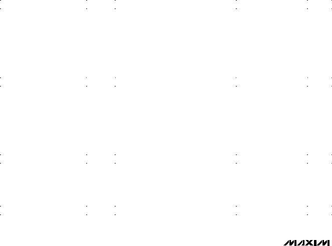
a) High-Z to VOH and VOL to VOH |
|
|
|
|
|
|
|
b) High-Z to VOL and VOH to VOL |
||||||||||||||||||
Figure 1. Load Circuits for DOUT Enable Time
|
|
|
|
|
|
|
|
|
|
|
|
|
|
|
|
+2.7V |
||||||||||
|
|
|
|
|
|
|
|
|
|
|
|
|
|
|
|
|
|
|
|
|
|
|
|
|
6k |
|
DOUT |
|
|
|
|
|
|
|
|
|
|
|
|
DOUT |
|
|
|
|
|
|
|
|
|
|
|
||
|
|
|
|
|
|
|
|
|
|
|
|
|
|
|
|
|
|
|
|
|
|
|||||
6k |
|
|
|
|
|
|
|
|
|
|
|
CLOAD = 50pF |
|
|
|
|
|
|
|
|
|
|
CLOAD = 50pF |
|||
|
|
|
|
|
|
|
|
|
|
|
|
|
|
|
|
|||||||||||
|
|
|
|
|
|
|
|
|
|
|
|
|
|
|
|
|||||||||||
|
|
|
|
|
|
DGND |
|
|
|
|
|
|
|
|
|
|
|
|
|
|
|
|
|
DGND |
||
|
|
|
|
|
|
|
|
|
|
|
|
|
|
|
|
|
|
|
|
|
||||||
|
|
|
|
|
|
|
|
|
|
|
|
|
|
|
|
|
|
|||||||||
|
|
|
|
|
|
|
|
|
|
|
|
|
|
|||||||||||||
a) VOH to High-Z |
|
|
|
|
|
|
|
|
|
|
|
|
b) VOLto High-Z |
|||||||||||||
|
|
|
|
|
|
|
|
|
|
|
|
|
|
|
|
|
|
|
|
|
|
|
|
|
|
|
Figure 2. Load Circuits for DOUT Disable Time
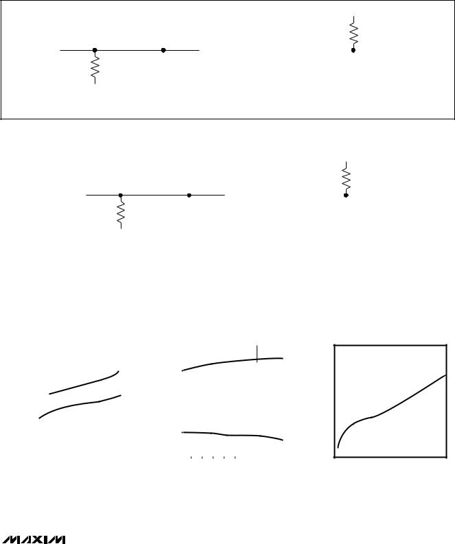
__________________________________________Typical Operating Characteristics
(VDD = 3.0V, VREF = 2.5V, fSCLK = 2.1MHz, CL = 20pF, TA = +25°C, unless otherwise noted.)
|
|
|
OPERATING SUPPLY CURRENT |
|
|
|
|
|
|
|
|
|
|
|
|
|
|
|
|
|
|
|
|
|
|
OFFSET ERROR |
||||||||||||
|
|
|
vs. SUPPLY VOLTAGE |
|
|
|
SUPPLY CURRENT vs. TEMPERATURE |
|
|
|
|
vs. SUPPLY VOLTAGE |
||||||||||||||||||||||||||
|
2.0 |
|
|
|
|
|
|
|
|
|
|
MAX1241-D |
1.3 |
|
|
|
|
|
|
|
|
|
|
|
|
|
|
MAX1241-A/NEW |
|
1.0 |
|
|
|
|
|
|
|
MAX1241-03 |
(mA) |
1.8 |
|
RL = ∞ |
|
|
|
|
|
|
|
|
|
|
|
|
|
|
|
|
|
|
MAX1240 |
|
|
|
|
0.9 |
|
|
|
|
|
|
|
||||
|
|
CODE = |
101010100000 |
|
|
|
|
|
|
|
|
|
|
|
|
|
|
|
|
|
|
|
|
|
|
|
|
|
|
|
|
|
|
|
|
|||
CURRENTSUPPLYOPERATING |
1.6 |
|
|
|
|
|
|
|
|
1.2 |
|
|
|
|
|
|
|
|
|
|
|
|
|
|
|
|
0.8 |
|
|
|
|
|
|
|
|
|||
|
|
|
|
|
|
|
|
|
|
|
|
|
|
|
|
|
|
|
|
|
|
|
|
|
|
|
|
|
|
|
|
|
|
|
||||
1.4 |
|
|
|
MAX1240 |
|
|
|
|
|
|
(mA)CURRENTSUPPLY |
|
|
|
|
|
|
|
|
|
|
|
|
|
|
|
(LSB)ERROROFFSET |
0.7 |
|
|
|
|
|
|
|
|
||
|
|
|
|
|
|
|
|
|
|
|
|
|
|
|
|
|
|
|
|
|
|
|
|
|
|
|
|
|
|
|
|
|
|
|
||||
|
1.2 |
|
|
|
|
|
|
|
|
|
|
|
1.1 |
|
|
|
|
|
|
|
|
|
|
|
|
|
|
|
|
0.6 |
|
|
|
|
|
|
|
|
|
|
|
|
|
|
|
|
|
|
|
|
|
|
|
|
|
|
|
|
|
|
|
|
|
|
|
|
|
|
|
|
|
|
|
|
|||
|
1.0 |
|
|
|
|
|
|
|
|
|
|
|
|
|
|
|
|
|
|
|
|
|
|
|
|
|
|
|
|
0.5 |
|
|
|
|
|
|
|
|
|
|
|
|
|
|
|
MAX1241 |
|
|
|
1.0 |
|
|
|
|
|
|
|
|
|
|
|
|
|
|
|
|
|
|
|
|
|
|
|
|
|||
|
0.8 |
|
|
|
|
|
|
|
|
|
|
|
|
|
|
|
|
|
|
|
|
|
|
|
|
|
0.4 |
|
|
|
|
|
|
|
|
|||
|
0.6 |
|
|
|
|
|
|
|
|
|
|
|
|
|
|
|
|
|
|
|
|
|
|
|
|
|
|
|
|
0.3 |
|
|
|
|
|
|
|
|
|
|
|
|
|
|
|
|
|
|
|
|
|
|
MAX1241 |
|
|
|
|
|
|
|
|
|
|
|
|
|
|
|
|
|
|
|
|
||||
|
0.4 |
|
|
|
|
|
|
|
|
|
|
|
|
|
|
|
|
|
|
|
|
|
|
|
|
|
0.2 |
|
|
|
|
|
|
|
|
|||
|
|
|
|
|
|
|
|
|
|
|
|
0.9 |
|
|
|
|
|
|
|
|
|
|
|
|
|
|
|
|
|
|
|
|
|
|
|
|
||
|
|
|
|
|
|
|
|
|
|
|
|
|
|
|
|
|
|
|
|
|
|
|
|
|
|
|
|
|
|
|
|
|
|
|
|
|||
|
0.2 |
|
|
|
|
|
|
|
|
|
|
|
|
RLOAD = ∞ |
|
|
|
|
|
|
|
|
|
|
|
0.1 |
|
|
|
|
|
|
|
|
||||
|
0 |
|
|
|
|
|
|
|
|
|
|
|
0.8 |
CODE = 10101010000 |
|
|
|
|
|
|
|
|
|
0 |
|
|
|
|
|
|
|
|
||||||
|
|
|
|
|
|
|
|
|
|
|
|
|
|
|
|
|
|
|
|
|
|
|
|
|
|
|
|
|
|
|
|
|
|
|
|
|||
|
2 |
3 |
4 |
|
5 |
|
6 |
-60 |
-20 |
|
20 |
60 |
100 |
|
140 |
|
|
2.25 2.75 3.25 3.75 4.25 4.75 5.25 |
||||||||||||||||||||
|
|
|
|
SUPPLY VOLTAGE (V) |
|
|
|
|
|
|
|
|
TEMPERATURE (°C) |
|
|
|
|
|
|
SUPPLY VOLTAGE (V) |
||||||||||||||||||
MAX1240/MAX1241
_______________________________________________________________________________________ 5
 Loading...