


LG LMS-U5050, LMS-U5050W, LMS-U5050S, LMS-U4050, LMS-U2350 User Manual
...
U5050S-LMS , U5050-LMS U5050-LMSW U5050A-LM, , U4050-LMS, U4050-LMSW U4050A-LM, U2350-LMS, U2350A-LM, MODEL ,AL MAN VICE :SE R U
3CD CHANGER
HI-FI SYSTEM
SERVICE MANUAL
CAUTION
BEFORE SERVICING THE UNIT, READ THE “SAFETY PRECAUTIONS” IN THIS MANUAL.
MODEL: LM-U2350A, LMS-U2350
LM-U4050A, LMS-U4050, LMS-U4050W
LM-U5050A, LMS-U5050, LMS-U5050W, LMS-U5050S

|
[CONTENTS] |
|
|
|
|
SECTION 1. GENERAL |
|
|
• SERVICING PRECAUTIONS . . . . . . . . . . . . . . . . . . . . . . . . . . |
. . . . . . . . . . . . . . . . . . . . . 1-2 |
|
• ESD PRECAUTIONS . . . . . . . . . . . . . . . . . . . . . . . . . . . . . . . . |
. . . . . . . . . . . . . . . . . . . . . 1-4 |
|
• SPECIFICATION . . . . . . . . . . . . . . . . . . . . . . . . . . . . . . . . . . . . |
. . . . . . . . . . . . . . . . . . . . . .1-5 |
|
SECTION 2. ELECTRICAL SECTION |
|
|
• ELECTRICAL TROUBLESHOOTING GUIDE . . . . . . . . . . . . . . |
. . . . . . . . . . . . . . . . . . . . . 2-1 |
|
• INTERNAL BLOCK DIAGRAM of ICs . . . . . . . . . . . . . . . . . . . . . |
. . . . . . . . . . . . . . . . . . . . 2-10 |
|
• BLOCK DIAGRAM . . . . . . . . . . . . . . . . . . . . . . . . . . . . . . . . . . |
. . . . . . . . . . . . . . . . . . . . 2-15 |
|
• SCHEMATIC DIAGRAMS . . . . . . . . . . . . . . . . . . . . . . . . . . . . . |
. . . . . . . . . . . . . . . . . . . . 2-19 |
|
• WIREING DIAGRAM . . . . . . . . . . . . . . . . . . . . . . . . . . . . . . . . . |
. . . . . . . . . . . . . . . . . . . . 2-43 |
|
• PRINTED CIRCUIT DIAGRAMS . . . . . . . . . . . . . . . . . . . . . . . . |
. . . . . . . . . . . . . . . . . . . . 2-45 |
|
SECTION 3. EXPLODED VIEWS
• CABINET AND MAIN FRAME SECTION . . . . . . . . . . . . . . . . . . . . . . . . . . . . . . . . . . . . . . . .3-1
• TAPE DECK MECHANISM (A/R & A/S : RIGHT A/R DECK) . . . . . . . . . . . . . . . . . . . . . . . . . .3-3
• TAPE DECK MECHANISM (A/R & A/S : LEFT A/S DECK) . . . . . . . . . . . . . . . . . . . . . . . . . . .3-5
• CD MECHANISM . . . . . . . . . . . . . . . . . . . . . . . . . . . . . . . . . . . . . . . . . . . . . . . . . . . . . . . . . 3-7
SECTION 4. SPEAKER PART
• SPEAKER PART . . . . . . . . . . . . . . . . . . . . . . . . . . . . . . . . . . . . . . . . . . . . . . . . . . . . . . . . . .4-1
SECTION 5. REPLACEMENT PARTS LIST
• REPLACEMENT PARTS LIST . . . . . . . . . . . . . . . . . . . . . . . . . . . . . . . . . . . . . . . . . . . . . . . .5-1
- 1-1 -
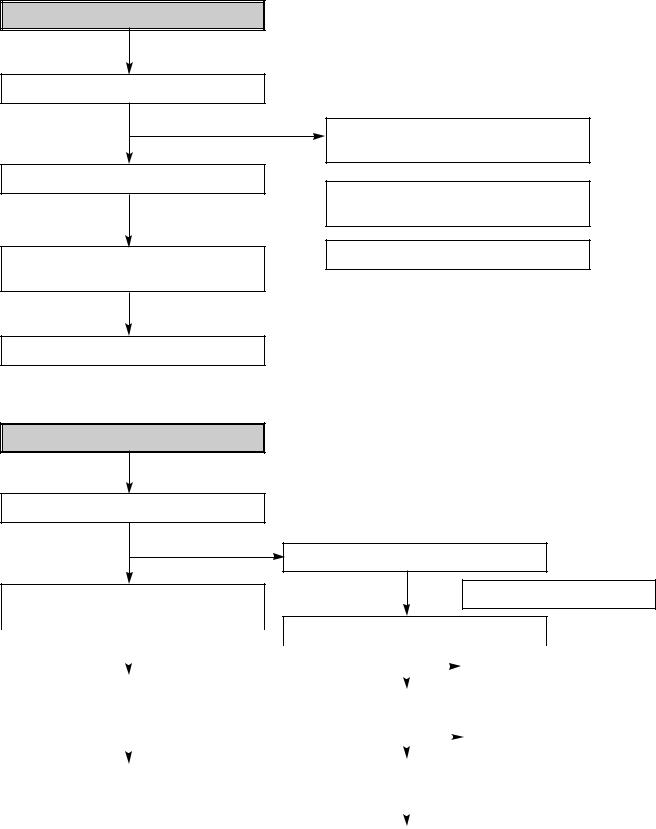
SECTION 1. GENERAL
SERVICING PRECAUTIONS
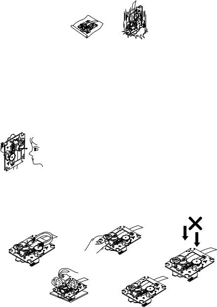
■ NOTES REGARDING HANDLING OF THE PICK-UP
1.Notes for transport and storage
1)The pick-up should always be left in its conductive bag until immediately prior to use.
2)The pick-up should never be subjected to external pressure or impact.
Storage in conductive bag |
Drop impact |
2.Repair notes
1)The pick-up incorporates a strong magnet, and so should never be brought close to magnetic materials.
2)The pick-up should always be handled correctly and carefully, taking care to avoid external pressure and impact. If it is subjected to strong pressure or impact, the result may be an operational malfunction and/or damage to the printed-circuit board.
3)Each and every pick-up is already individually adjusted to a high degree of precision, and for that reason the adjustment point and installation screws should absolutely never be touched.
4)Laser beams may damage the eyes!
Absolutely never permit laser beams to enter the eyes!
Also NEVER switch ON the power to the laser output part (lens, etc.) of the pick-up if it is damaged.
NEVER look directly at the laser beam, and don’t let contact fingers or other exposed skin.
5)Cleaning the lens surface
If there is dust on the lens surface, the dust should be cleaned away by using an air bush (such as used for camera lens). The lens is held by a delicate spring. When cleaning the lens surface, therefore, a cotton swab should be used, taking care not to distort this.
Pressure
Magnet
Pressure
How to hold the pick-up
Cotton swab 
Conductive Sheet
6)Never attempt to disassemble the pick-up.
Spring by excess pressure. If the lens is extremely dirty, apply isopropyl alcohol to the cotton swab. (Do not use any other liquid cleaners, because they will damage the lens.) Take care not to use too much of this alcohol on the swab, and do not allow the alcohol to get inside the pick-up.
-1-2 -
■ NOTES REGARDING COMPACT DISC PLAYER REPAIRS
1. Preparations
1)Compact disc players incorporate a great many ICs as well as the pick-up (laser diode). These components are sensitive to, and easily affected by, static electricity. If such static electricity is high voltage, components can be damaged, and for that reason components should be handled with care.
2)The pick-up is composed of many optical components and other high-precision components. Care must be taken, therefore, to avoid repair or storage where the temperature of humidity is high, where strong magnetism is present, or where there is excessive dust.
2. Notes for repair
1)Before replacing a component part, first disconnect the power supply lead wire from the unit
2)All equipment, measuring instruments and tools must be grounded.
3)The workbench should be covered with a conductive sheet and grounded.
When removing the laser pick-up from its conductive bag, do not place the pick-up on the bag. (This is because there is the possibility of damage by static electricity.)
4)To prevent AC leakage, the metal part of the soldering iron should be grounded.
5)Workers should be grounded by an armband (1M Ω)
6)Care should be taken not to permit the laser pick-up to come in contact with clothing, in order to prevent static electricity changes in the clothing to escape from the armband.
7)The laser beam from the pick-up should NEVER be directly facing the eyes or bare skin.
Armband
 Resistor
(1 Mohm)
Resistor
(1 Mohm)
Conductive
Sheet
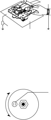
CLEARING MALFUNCTION
You can reset your unit to initial status if malfunction occur(button malfunction, display, etc.).
Using a pointed good conductor(such as driver), simply short the RESET jump wire on the inside of the volume knob for more than 3 seconds.
If you reset your unit, you must reenter all its settings(stations, clock, timer)
NOTE: 1. To operate the RESET jump wire, pull the volume rotary knob and release it.
2. If you wish to operate the RESET jump wire, it is necessary to unplug the power cord.
VOLUME
UP |
RESET jump wire |
|
|
VOLUME KNOB |
|
DOWN |
|
- 1-3 -
ESD PRECAUTIONS
■ Electrostatically Sensitive Devices (ESD)
Some semiconductor (solid state) devices can be damaged easily by static electricity. Such components commonly are called Electrostatically Sensitive Devices (ESD). Examples of typical ESD devices are integrated circuits and some field-effect transistors and semiconductor chip components. The following techniques should be used to help reduce the incidence of component damage caused by static electricity.
1.Immediately before handling any semiconductor component or semiconductor-equipped assembly, drain off any electrostatic charge on your body by touching a known earth ground. Alternatively, obtain and wear a commercially available discharging wrist strap device, which should be removed for potential shock reasons prior to applying power to the unit under test.
2.After removing an electrical assembly equipped with ESD devices, place the assembly on a conductive surface such as aluminum foil, to prevent electrostatic charge buildup or exposure of the assembly.
3.Use only a grounded-tip soldering iron to solder or unsolder ESD devices.
4.Use only an anti-static solder removal device. Some solder removal devices not classified as "anti-static" can generate electrical charges sufficient to damage ESD devices.
5.Do not use freon-propelled chemicals. These can generate electrical charges sufficient to damage ESD devices.
6.Do not remove a replacement ESD device from its protective package until immediately before you are ready to install it. (Most replacement ESD devices are packaged with leads electrically shorted together by conductive foam, aluminum foil or comparable conductive materials).
7.Immediately before removing the protective material from the leads of a replacement ESD device, touch the protective material to the chassis or circuit assembly into which the device will by installed.
CAUTION : BE SURE NO POWER IS APPLIED TO THE CHASSIS OR CIRCUIT, AND OBSERVE ALL OTHER SAFETY PRECAUTIONS.
8.Minimize bodily motions when handing unpackaged replacement ESD devices. (Otherwise harmless motion such as the brushing together of your clothes fabric or the lifting of your foot from a carpeted floor can generate static electricity sufficient to damage an ESD device).
CAUTION. GRAPHIC SYMBOLS
THE LIGHTNING FLASH WITH APROWHEAD SYMBOL. WITHIN AN EQUILATERAL TRIANGLE, IS INTENDED TO ALERT THE SERVICE PERSONNEL TO THE PRESENCE OF UNINSULATED “DANGEROUS VOLTAGE” THAT MAY BE OF SUFFICIENT MAGNITUDE TO CONSTITUTE A RISK OF ELECTRIC SHOCK.
THE EXCLAMATION POINT WITHIN AN EQUILATERAL TRIANGLE IS INTENDED TO ALERT THE SERVICE PERSONNEL TO THE PRESENCE OF IMPORTANT SAFETY INFORMATION IN SERVICE LITERATURE.
- 1-4 -
SPECIFICATIONS
SECTION |
MODEL |
||
|
|||
|
[General] |
Power supply |
|
|
Power consumption |
|
|
|
|
|
|
|
|
Weight |
|
|
|
External dimensions (W x H x D) |
|
|
[CD] |
Frequency response |
|
|
Signal-to-noise ratio |
|
|
|
|
|
|
|
|
Dynamic range |
|
|
|
Tuning Range |
|
|
|
|
|
|
FM |
Intermediate Frequency |
|
[Tuner] |
Signal to Noise Ratio |
|
|
AM (MW) |
Frequency Response |
|
|
|
|
|
|
|
|
Tuning Range |
|
|
|
Intermediate Frequency |
|
|
|
Signal to Noise Ratio |
|
|
|
Frequency Response |
|
|
[Amp] |
Output Power |
|
|
T.H.D |
|
|
|
|
|
|
|
|
Frequency Response |
|
|
|
Signal-to-noise ratio |
|
|
|
Tape Speed |
|
|
|
Wow Flutter |
|
|
TAPE[ ] |
F.F/REW Time |
|
|
Frequency Response |
|
|
|
|
|
|
|
|
Signal to Noise Ratio |
|
|
|
Channel Separation |
|
|
|
Erase Ratio |
|
|
|
Speaker Name |
|
|
|
Type |
|
|
Speakers[ ] |
Impedance |
|
|
Frequency Response |
|
|
|
|
|
|
|
|
Sound Pressure Level |
|
|
|
Rated Input Power |
|
|
|
Max. Input Power |
|
|
|
Net Dimensions (W x H x D) |
|
|
|
Weight |
|
|
|
Speaker Name |
|
|
|
Type |
|
|
[Subwoofer] |
Impedance |
|
|
Frequency Response |
|
|
|
|
|
|
|
|
Sound Pressure Level |
|
|
|
Rated Input Power |
|
|
|
Max. Input Power |
|
|
|
Net Dimensions (W x H x D) |
|
|
|
Weight |
|
|
|
|
|
LM-U5050 |
|
LM-U4050 |
|
LM-U2350 |
|
|
|
|
|
Refer to the back panel of the unit. |
|
|
||
|
200 W |
|
110 W |
|
|
|
|||
8.5 kg
280 x 370 x 400 mm
40 - 18000 Hz
75 dB
70 dB
87.5- 108.0 MHz or 65 - 74 MHz, 87.5 - 108.0 MHz
10.7MHz
60/55 dB
60 - 10000 Hz
522 - 1620 kHz or 520 - 1720 kHz
450 kHz
30 dB
120 - 2000 Hz
Front : 270 W + 270 W (LM-U5050 model only)
250 W + 250 W (LM-U4050/U2350 model only) Surround : 110 W + 110 W (LM-U5050 model only) Subwoofer : 350 W (LM-U5050/U4050 model only)
0.7%
42 - 20000 Hz
80 dB
3000 ± 3 % (MTT-111. NORMAL-SPEED)
0.25 % (MTT -111, JIS-WTD)
120 sec (C-60)
125 - 8000 Hz
40 dB
50 dB (P/B)/45 dB (R/P)
55dB (MTT-5511)
Front speaker (L/R) |
Surround speaker (L/R) |
||
LMS-U5050 |
LMS-U4050/U2350 |
[LMS-U5050S] |
|
Bass Reflex 3Way 3 Speaker |
Bass Reflex 2Way 2Speaker |
||
|
|
6Ω |
24Ω |
55 - 20000 Hz |
60 - 20000 Hz |
||
|
86 dB/W (1m) |
86 dB/W (1m) |
|
270 W |
|
250 W |
110 W |
|
|||
540 W |
|
500 W |
220 W |
250 X |
300 X 415 mm |
187 X 258 X 415 mm |
|
|
|
9.3 kg |
4.3 kg |
Subwoofer (LMS-U5050W/U4050W)
1 Way 1 Speaker
6Ω
45 - 15000 Hz
84 dB/W (1m)
350 W
700 W
279 X 320 X 415 mm
10.0 kg
- 1-5 -

- 1-6 -
SECTION 2. ELECTRICAL
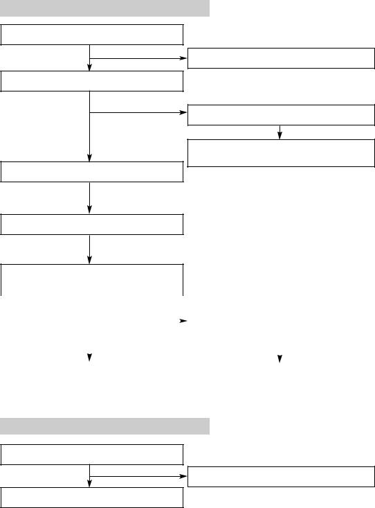
ELECTRICAL TROUBLESHOOTING GUIDE
■ SMPS POWER CIRCUIT
P-SENS PART
SMPS ASSY CN902 7PIN 5.1V CHECK
YES NO
MAIN PCB CN710 7PIN 5.1V CHECK
NO
YES
MAIN PCB CN304 5PIN 5.1VCHECK
YES
FRONT PN302 36PIN 5.1VCHECK
YES
FRONT IC306(RESET IC)
STATE CHECK
SMPS TROUBLESHOOTING CONSULT
CN710 CONNECTION STATE CHECK
MAIN PCB PATTERN CUTTING AND
SHORT CHECK
|
NO |
|
|
|
|
|
IC306 INPUTVOLTAGE4V, |
||||
YES |
|
|
|
||
|
|
|
OUTPUTVOLTAGE.2.1VSTATECHECK |
||
|
|
|
|
|
|
|
|
|
|
|
|
|
|
|
|
|
|
U-COM IC304 26PIN 5VCHECK |
|
IC306 KIA7042 CHANGE |
|
|
|
VKK CHECK
CN710 10PIN DC -33V CHECK
NO
YES
IC304 51PIN VOLTAGE CHECK
SMPS TROUBLESHOOTING CONSULT
- 2-1 -
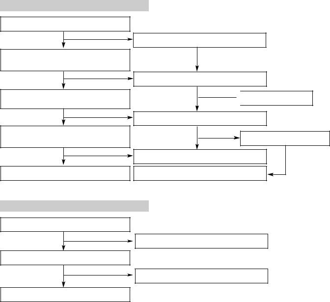
MICOM (IC301) CHECK
"P-SENS" CHECK
YES |
NO |
P-SENS TROUBLESHOOTING CONSULT |
"RESET" IC304 11 PIN CHECK (HIGH LOW HIGH)
YES NO
IC304 VDD(17,46,72,90) PIN VOLTAGE
CHECK
YES NO
X301 VIBRATION SIGNAL CHECK
NO
YES
IC301 CHANGE
Q303 STATE CHECK
 TR "Q303" CHANGE
PN302 35 PIN +5.6V(MI) CHECK
MAIN CN710 6 PIN CHECK
X301 CHANGE
SMPS TROUBLESHOOTING CONSULT
P-CTRL CHECK
PN302 33 PIN "P-CTRL" CHECK (HIGH)
YES NO
CN710 5 PIN CHECK
NO
YES
SMPS TROUBLESHOOTING CONSULT
MICOM IC304 STATE CHECK
SMPS + MAIN BORD-TO-BORD CHECK
- 2-2 -
MUTING TROUBLESHOOTING (MUTE STATE)
Q752(A102) BASE "HIGH"
YES NO
Q701, Q751(D1302) BASE "HIGH"
CHECK
NO
YES
EXPEND IC(IC305) 5PIN HIGH STATE CHECK
YES
Q752(A102)STATE CHECK
YES
Q752(A102) FAULTY IS CHANGE
YES
EACH PART TR CHANGE
MUTE
EXPEND IC(IC305/501/502) STATE
16 PIN VDD VOLTAGE CHECK
YES |
|
NO |
|
|
|
|
|
|
|
|
|
|
D332/D553/D551(1SS133) CHECK |
|
|||||||
|
|
|
|
|
||||||
|
|
|
|
|
|
|||||
|
|
|
|
|
|
|
|
|
|
|
3 "EXP-CLK" CHECK |
|
YES |
NO |
|
D332/D553/D551(1SS133) |
|||||
|
|
|
|
|
|
|
|
CHANGE |
||
YES |
|
NO |
|
|
|
|
|
|||
|
|
|
|
|
|
|
|
|||
|
|
|
|
|
|
|
|
|
|
|
|
|
|
MICOM (IC304) 4/84/85 PIN |
|
|
|||||
|
|
|
|
|
|
|
||||
|
|
|
|
|
|
|
||||
|
|
|
|
|
CHECK(CLK1/2/3) |
|
|
|||
|
|
|
|
|
|
|
||||
2 "EXP-DATA" CHECK |
|
|
NO |
|
|
|
||||
|
YES |
|
PCB PATTERN CHECK |
|||||||
|
|
|
|
|
|
|
|
|||
|
|
|
|
|
|
|
|
|||
|
|
|
|
|
|
|
|
|
|
|
YES |
|
NO |
|
|
|
|
|
|
|
|
|
|
|
|
|
|
|
|
|||
|
|
|
|
|
MICOM (IC304) 3 PIN CHECK |
|
|
|||
|
|
|
|
|
|
|
||||
|
|
|
|
|
|
|
|
|
|
|
|
|
|
|
|
|
NO |
|
|
|
|
4 PIN ~ 15 PIN EACH PORT STATE |
|
|
||||||||
|
YES |
|
PCB PATTERN CHECK |
|||||||
|
|
|
|
|||||||
CHECK |
|
|
|
|
|
|
||||
|
|
|
|
|
|
|||||
|
|
|
|
|
|
|
|
|
||
|
|
|
|
|
|
|
|
|
|
|
YES |
|
NO |
|
|
|
|
|
|
|
|
|
|
|
|
|
|
|
|
|||
|
|
|
|
EXPEND IC FAULTY IS CHANGE |
|
|||||
|
|
|
|
|
||||||
|
|
|
|
|
|
|
|
|
|
|
EXPEND IC OK
- 2-3 -
SPECIFIC FUNCTION MODE HAS NO SOUND (NJW1190) IC601
IC201 INPUT CHECK(HEAD
INPUT)"A"DECK 32,39 "B"DECK 34,37
|
YES |
|
|
NO |
|
DECK HEAD WIRE |
|
|
|
|
|
||||||
|
|
|
|
|
|
|
|
CONNECTION STATE CHECK |
|
|
|
|
|
||||
|
|
|
|
|
|
|
|
|
|
|
|
|
|
|
|||
|
|
|
|
|
|
|
|
|
|
|
|
|
|
|
|
|
|
|
IC201 OUTPUT CHECK(5,26 PIN) |
|
|
|
|
|
|
|
|
|
|
|
|||||
|
|
|
|
|
|
|
|
|
|
|
|
|
|
|
|
|
|
|
YES |
|
|
NO |
|
|
|
|
|
|
|
|
|||||
|
|
|
IC502 10PIN(PB MUTE) STATE |
|
|
|
|
|
|||||||||
|
|
|
|
|
|
|
|
|
|
|
|
||||||
|
|
|
|
|
|
|
|
|
|
STATE CHECK |
|
|
NO |
||||
|
|
|
|
|
|
|
|
|
|
|
|
||||||
|
|
|
|
|
|
|
|
|
|
|
|
|
|
|
|||
IC601 3,36PIN INPUT SIGNAL CHECK |
|
|
|
YES |
|
|
|
||||||||||
|
|
|
|
|
|
1) |
|||||||||||
|
|
|
|
|
|
||||||||||||
|
|
|
|
|
|
|
|
|
|
|
|
|
|
|
|
|
|
|
YES |
|
|
NO |
|
|
|
|
|
|
|
|
|||||
|
|
|
|
|
|
|
|
|
|
||||||||
IC502 4PIN(REC SW) "HIGH" |
|
|
IC502 4PIN(REC SW) "LOW" |
||||||||||||||
|
|
|
|
|
|
|
|
|
|
|
|
||||||
|
|
|
|
|
|
|
|
|
|
|
CHECK |
|
|
STATE REC |
|||
|
|
|
|
|
|
|
|
|
|
|
|
|
|||||
|
|
|
|
|
|
|
|
|
|
|
|
|
|
|
|
|
|
|
|
|
|
|
|
|
|
|
|
|
|
|
|
|
|||
IC601 17,22 PIN OUTPUT SIGNAL |
|
|
|
|
|
|
|
|
YES |
|
|
||||||
|
CHECK |
|
|
|
|
|
|
|
|
|
|
|
|
|
|||
|
|
|
|
|
|
|
|
|
|
|
|
|
|
|
|
|
|
|
YES |
|
|
NO |
|
|
|
IC601(NJW1190) |
|
|
Q212 (C) "HIGH" CHECK |
||||||
|
|
|
|
|
|
|
|
TROUBLESHOOTING CONSULT |
|
|
|||||||
|
|
|
|
|
|
|
|
|
|
|
|
|
|
|
|||
|
DECK OUTPUT |
|
|
|
|
|
|
|
|
YES |
|
|
|||||
|
|
|
|
|
|
|
|
|
|
|
|
||||||
|
|
|
|
|
|
|
|
|
|
|
|
|
|
|
|
|
|
|
|
|
|
|
|
|
|
|
|
|
|
|
|
|
|
|
|
|
|
|
|
|
|
|
|
|
|
|
|
|
|
|
Q213 (C) "LOW" CHECK |
||
|
|
|
|
|
|
|
|
|
|
|
|
|
|
|
|
|
|
|
|
|
|
|
|
|
|
|
|
|
|
|
|
|
YES |
|
|
|
|
|
|
|
|
|
|
|
|
|
|
|
|
|
|
|
|
|
|
|
|
|
|
|
|
|
|
|
|
|
|
|
|
|
|
1) |
|
|
|
|
IC502 2 PIN/3 PIN |
|
|
|
|
IC502 13 PIN "REC-BAIS" HIGH |
|||||||
|
|
|
|
CHECK(DATA/CL |
|
|
|
|
CHECK |
||||||||
|
|
|
|
|
|
|
|
||||||||||
|
|
|
|
|
|
|
|
|
|||||||||
|
|
|
|
|
YES |
|
|
|
|
|
|
|
|
|
YES |
|
|
|
|
|
|
|
|
|
|
|
|
|
|
|
|
|
|
||
|
|
|
|
|
|
|
|
|
|
|
|
|
|||||
|
|
|
|
|
|
|
|
|
|
|
|
|
|
|
|
|
|
|
|
|
|
|
|
|
|
|
|
|
|
|
|
|
L203(4.7MH) COIL VIBRATION |
||
|
|
|
|
|
IC502 16 PIN VDD CHECK |
|
|
|
|
SIGNAL CHECK |
|||||||
|
|
|
|
|
|
|
|
|
|
|
|
|
|
|
|
|
|
|
|
|
|
|
|
|
|
|
|
|
|
|
|
|
YES |
|
|
|
|
|
|
|
YES |
|
|
|
|
|
|
|
|
|
|
|
|
|
|
|
|
|
|
|
|
|
|
|
|
|
|
|
|
||
|
|
|
|
|
|
|
|
|
|
|
|
|
|||||
|
|
|
|
|
|
|
|
|
|
|
|
|
|
|
IC601 7 /32 INPUT REC' |
||
|
|
|
|
|
|
|
|
|
|
|
|
|
|
|
|||
|
|
|
|
|
|
|
|
|
|
|
|
|
|
|
SIGNAL CHECK |
||
|
|
|
|
|
IC502 EXPEND IC CHANGE |
|
|
|
|
||||||||
|
|
|
|
|
|
|
|
|
|
|
|
||||||
|
|
|
|
|
|
|
|
|
|
||||||||
|
|
|
|
|
|
|
|
|
|
|
|
|
|
|
|
|
|
- 2-4 -
AUX
YES
JK601 SIGNALINPUT CHECK
YES
IC601 5,34 PIN SIGNALINPUTCHECK
YES NO
IC601 17,22 PIN OUTPUT SIGNAL
CHECK
NO
YES
AUX OUTPUT
CD
YES
CN709 1,3PIN SIGNALCHECK CD TROUBLESHOOTINGCONSULT
YES
IC601 4,35PIN SIGNALINPUTCHECK
YES NO
IC601 17,22 PIN OUTPUT SIGNAL
CHECK
YES NO
CD OUTPUT
MAIN PCB PATTERN CHECK
IC601(NJW1190)
TROUBLESHOOTING CONSULT
MAIN PCB PATTERN CHECK
IC601(NJW1190)
TROUBLESHOOTING CONSULT
- 2-5 -
TUNER
YES
TU101 3 /5 SIGNAL CHECK
YES NO
IC601 2,37 PIN SIGNALINPUTCHECK
YES
IC601 17,22 PIN OUTPUT SIGNAL
CHECK
YES
TUNER OUTPUT
TU101 2 PIN "+9V"
VOLTAGE CHECK
TU101 6,7,8,9 PIN CHECK (PLL-CE, PLL-DI, CLK, PLL-DO)
TUNER MODULE CHANGE
MIC
YES
CN303 7 PIN "MIC-SIGNAL" CHECK
<MIC PCB>
YES NO
CN303 4 MIC-SENSE CHECK
NO
IC601 44 PIN SIGNAL CHECK(OW601 YES  PN400 3 PIN "+12V"CHECK PATTERN)
|
|
|
IC402 8 PIN SIGNAL INPUT CHECK |
||||||||
YES |
|
||||||||||
|
|
|
|
|
|
|
|
|
|
|
|
|
YES |
NO |
|
|
|
|
|
||||
|
|
|
|
MIC MUTE CHECK(Q409/ Q408) |
|||||||
|
|
|
|
|
|
|
|||||
IC601 17,22 PIN OUTPUT SIGNAL |
|
|
|
|
|
|
|
|
|
|
|
|
|
|
|
|
|
|
|
|
|
||
|
PN400 9 "VOL-IN"CHECK |
|
|
|
|||||||
CHECK |
|
|
|
|
|||||||
|
|
|
|
|
|
|
|
|
|
|
|
YES |
|
|
YES |
NO |
|
TR CHANGE |
|
||||
|
|
|
|
|
|
|
|
||||
|
|
|
|
|
|
|
|
|
|
|
|
|
|
|
|
|
|
|
|
|
|
|
|
|
|
|
IC402 2 PIN SIGNAL INPUT CHECK |
|
|
||||||
MIC OUTPUT |
|
|
|
||||||||
|
|
|
|
|
|
|
|
|
|
||
|
|
|
YES |
|
|
|
|
|
|
|
|
|
|
|
|
|
|
|
|
|
|
|
|
|
|
|
|
|
|
|
|
|
|
||
|
|
|
|
|
|
|
|
|
|
|
|
|
|
|
PN400 10 PIN "VOL-OUT"CHECK |
|
|
|
|||||
|
|
|
|
|
|
|
|
|
|
|
|
|
|
- 2-6 - |
|
|
|
|
|
|
|
|
|
IC601(NJW1190) TROUBLESHOOTING
IC601 24PIN VOLTAGE INPUT CHECK
NO
YES  SMPS VOLTAGE CHECK CONSULT
IC601 19,20 SDA, SCA PULSE WAVE CHECK (VOL UP, DOWN TURN CHECK)
NO
YES
FUNCTION INPUT PORT SIGNAL CHECK(NJW1190 TROUBLESHOOTING)
YES NO
IC601 17.22 PIN WAVE OUTPUT CHECK
YES
IC601 OK
AMP MODULE TROUBLESHOOTING
IC501 9 PIN(AMP-PWR)HIGH CHECK
NO
YES
IC305 9 PIN(AMP-PWR) HIGH CHECK
YES
PN702 3 PIN "PROTECTION"CHECK
(HIGH LOW)
NO
YES
IC701 11 PIN "AMP-ON/OFF" HIGH
CHECK
YES
IC701 12 PIN "PROTECTION" LOW
CHECK
YES
IC701 3 ,20 & 5 ,18 EACH +65V &-65V
CHECK
NO
YES
IC301 10,8PIN CHECK
IC301 TROUBLESHOOTING
IC601 CHANGE
EXPEND IC TROUBLESHOOTING CONSULT
PROTECTION " HIGH" SMPS VOLTAGE AND AMP ON/ OFF STATE CHECK
AMP MODULE CHECK : MOS FET BOTH ARE READ SHORT AMP DEAD
AMP MODULE CHANGE
SMPS TROUBLESHOOTING CONSULT
- 2-7 -
IC701 9 ,14 ±9V CHECK
NO
YES |
|
SMPS TROUBLESHOOTING CONSULT |
|
IC701 10 , 13 INPUT SIGNAL CHECK
YES
IC701 5 ,17 OUTPUT SIGNAL CHECK
YES
OK
REC CHECK (Q252,Q202 ON :R273,R223 HIGH)
IC601 24PIN VOLTAGE INPUT CHECK
YES
IC401 EACH INPUTTUNER6,39.TAPE. 7.38.CD. 8.38.AUX.9.36 PIN SIGNAL INPUT CHECK
NO
YES
IC201 7,24 PIN INPUT CHECK
YES |
NO |
|
|
|
|
|
|
|
IC201 10.21 PIN OUTPUT CHECK
YES |
NO |
|
|
|
|
L203 2,3PIN CHECK
NO
YES
IC202 14 PIN STATESTATE CHECK
YES
Q213.212 STATE STATECHECK
YES
DECK CHANGE
REC INPUTCHECK CHECK
INPUT LINE CHECK
REC OUTPUTCHECK AFTER FAULTY IS ICCHANGE
IC202 4PIN STATECHECK
NO |
VOLTAGE CHECK CONSULT |
|
Q205 BASE 0.6V CHECK
NO |
|
IC202 TROUBLESHOOTING CHECK |
|
Q204 COLLECTOR LOW |
|
NO |
Q204 CHANGE |
|
|
Q203 CHANGE |
|
NO |
L203 CHANGE |
|
OK
- 2-8 -
DUBBING CHECK ("NORMAL OR REC"//"HIGH")
IC401 11,34 OUTCHECK
YES
IC401 EACH INPUTTUNER6,39.TAPE. 7.38.CD.8.38.AUX.9.36PIN SIGNAL
INPUT CHECK
NO
YES |
REC INPUTCHECK CHECK |
|
IC201 7,24 PIN INPUT CHECK
NO
YES |
|
INPUT LINE CHECK |
|
IC201 10.21PIN OUTPUT CHECK
- 2-9 -
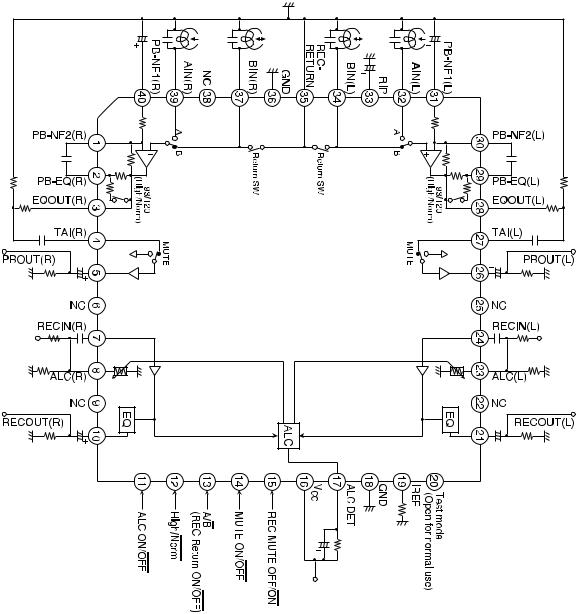
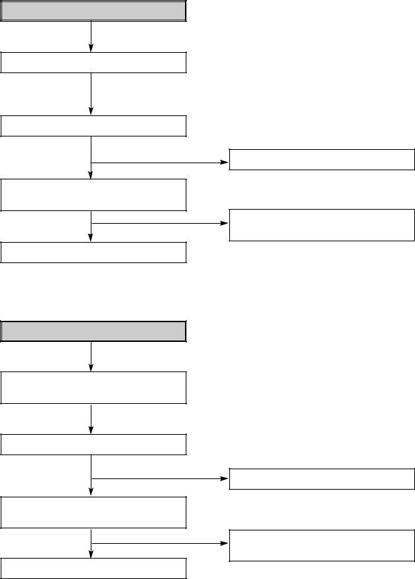
INTERNAL BLOCK DIAGRAM of ICs
• HA12237F
BLOCK DIAGRAM
- 2-10 -
 Loading...