


User’s Manual
LG Programmable Logic Controller
G3F-AD3A
G4F-AD3A
G6F-AD2A
 LG Industrial Systems
Safety Precautions
Safety Precautions
Be sure to read carefully this safety precaution given in data sheet and user’s manual before operating the module and follow them.
The precautions explained here only apply to the G3F-AD3A, G4F-AD3A, and G6F-AD2A.
For safety precautions on the PLC sys tem, please see the MASTER-K 200S/300S/1000S User’s manual and the GLOFA GM3/4/6 User’s manual.
A precaution is given with a hazard alert triangular symbol to call your attention, and precautions are represented as follows according to the degree of hazard.
WARNING
CAUTION
However, a precaution followed with
If not provided with proper prevention, it can cause death or fatal injury or considerable loss of property.
If not properly observed, it can cause a hazard situation to result in severe or slight injury or a loss of property.
 CAUTION can also result in serious conditions.
Both of two symbols indicate that an important content is mentioned, therefore, be sure to observe it.
Keep this manual handy for your quick reference in necessary.
Design Precautions
CAUTION
Do not run I/O signal lines near to high voltage line or power line. Separate them as 100mm or more as possible. Otherwise, noise can cause module malfunction.
Installation Precautions
CAUTION
Operate the PLC in the environment conditions given in the general specifications
If operation in other environment not specified, it can cause an electric shock, a fire, malfunction or damage or degradation of the module.
Make sure the module fixing projections is inserted into the module fixing hole and fixed.
Improper installation of the module can cause malfunction, disorder or falling.
Safety Precautions
Wiring Precautions
CAUTION
When grounding a FG terminal, be sure to provide class 3 grounding which is dedicated to the PLC.
Before the PLC wiring, be sure to check the rated voltage and terminal arrangement for the module and observe them correctly. If a different power, not of the rated voltage, is applied or wrong wiring is provided, it can cause a fire or disorder of the module.
Fasten the terminal screws firmly to the defined torque. If loosely fasten, it can cause short circuit, a fire or malfunction.
Be careful that any foreign matter like wire scraps should not enter into the module. It can cause a fire, disorder or malfunction.
Test Run and Maintenance Precautions
CAUTION |
WARNING |
Do not contact the terminals while the power is applied. It can cause malfunction.
When cleaning or driving a terminal screw, perform them after the power has been turned off.
Do not perform works while the power is applied, which can cause disorder or malfunction.
Do not separate the module from the printed circuit board (PCB), or remodel the module. Th ey can cause disorder, malfunction, damage of the module or a fire.
When mounting or dismounting the module, perform them after the power has been turned off.
Waste Disposal Precautions
CAUTION
When disposing the module, do it as anindustrial waste.

CONTENTS
Chapter 1. INTRODUCTION
1.1Features ···································································································································1-1
1.2Terminology ·····························································································································1-2
1.2.1Analog Value : A ·······················································································································1-2
1.2.2Digital Value : D ························································································································1-2
1.3Analog to Digital Conversion Characteristics ····································································1-3
1.3.1Voltage input····························································································································1-3
1.3.2Current input····························································································································1-5
Chapter 2. SPECIFICATIONS
2.1General Specifications ··········································································································2-1
2.2Performance Specifications ·································································································2-2
2.3 Names of Parts and Functions ·····························································································2-4
2.3.1G3F-A D3A ·····························································································································2-4
2.3.2G4F-A D3A ·····························································································································2-5
2.3.3G6F-A D2A ·····························································································································2-6
2.4 I/O Conversion Characteristics ····························································································2-7
2.4.1 |
Voltage Input Characteristics |
····································································································2-8 |
2.4.2 |
Current Input C haracteristics |
···································································································2-10 |
2.4.3 |
Simultaneous Voltage and Current Input Characteristics ·································································2-11 |
|
2.4.4 Analog input and Digital output characteristics ·············································································2-12
2.5Processing Specification·······································································································2-13
2.5.1 Sampling processing A/D conversion system ················································································2-13
2. 5.2 Averaging processing A/D conversion system ···············································································2-13
Chapter 3. INSTALLATION AND WIRING
3.1Installation ·····························································································································3-1
3.1.1Installation Ambience·················································································································3-1
3.1.2Handling Precautions ···············································································································3-1

3.2Wiring ····································································································································3-2
3.2.1Wiring Precautions ··················································································································3-2
3.2.2Wiring Examples ·····················································································································3-2
Chapter 4. FUNCTION BLOCK
4.1 Registration of the Function Block for the A/D Conversion Module on the GMWIN ·······4-1
4.2Function Block for Local········································································································4-2
4.2.1Module Initialization ·················································································································4-2
4.2.2 Module Read ing - Array Type ····································································································4-4
4.2.3Module Read ing - Single Type·····································································································4-5
4.3Remote Function Block ········································································································4-6
4.3.1Module Initialization ·················································································································4-6
4.3.2Module Read ing ·······················································································································4-8
4.4 Errors on Function Block ····································································································4-10
Chapter 5. GM PROGRAMMING
5.1Programming for Distinction of A/D Conversion Value ·······················································5-1
5.2Programming for Display of A/D Conversion Value and Error Code on BCD Display...····5-5
5.3 Programming for Loading the A/D Conversion Module on Remote I/O Station ···············5-8
Chapter 6. Buffer Memory
6.1The configuration of buffer memory ·····················································································6-1
6.1.1G6F-AD2A ······························································································································6-1
6.1.2 G3F-AD3A / G4F-AD3A ·············································································································6-2
6.2The contents and description of buffer memory ··································································6-3
6. 2.1 G6F-AD2A ······························································································································6-3
6. 2.2 G3F-AD3A / G4F-AD3A ·············································································································6-8
Chapter 7. Buffer read/write instructions
7.1Buffer read instructions··········································································································7-1
7.1.1 GET/GETP instruction················································································································7-1
7.1.2 RGET instruction······················································································································7-3
7.2Buffer write instructuins ·········································································································7-6
7. 2.1 |
PUT/PUTP instruction ················································································································7-6 |
7. 2.2 |
RPUT instruction ······················································································································7-8 |

Chapter 8. MK Programming
8.1Basic Programming ···············································································································8-1
8.1.1G6F-AD2A ·····························································································································8-1
8.1.2 G 3F -A D3A / G4F-AD3A ············································································································8-2
8.2 Example Programming ·········································································································8-3
8.2.1 A program for comparision of A/D conversion value ········································································8-3 8.2.2 Output the analog input value by 7-segment display ·······································································8-5 8.2.3 An A/D module mounted on a remote station ··················································································8-7
Chapter 9. DIMENSIONS
9.1G3F-AD3A Dimensions ·········································································································9-1
9.2G4F-AD3A Dimensions ·········································································································9-2
9.3G6F-AD2A Dimensions ·········································································································9-3

Chapter 1 Introduction
1 |
Introduction |
|
|
|
|
T h e G 3 F -A D 3 A , G 4 F -A D 3 A , a n d G 6 F-AD2A modules are analog-to-dgital conversion |
|||
|
modules for use with the GLOFA PLC |
GM1/2/3/4/6 series and M A S T E R -K |
P L C |
|
|
K 2 0 0 S /3 0 0 S /1000S series. The G3F -A D 3 A |
is u s e d w ith G M 1 /2 /3 series and |
K1000S |
|
|
series, G 4 F -A D 3 A is used with GM4 series and K300S series, and G6F-A D 2 A |
is |
used |
|
|
w ith GM6 series and K200S series. (Hereafter the G3F-A D 3 A , G 4 F -A D 3 A , a n d |
G 6 F- |
||
|
AD2A modules are called as the A/D conversion m o d u le) |
|
|
|
The A/D conversion m o d u le is to convert an analog input sig nal (voltage or current) from external devices into a 12-bitsigned binary digital value.
1.1Features
1)M u lti-channel analog to digital conversion is possible with a single A/D m o d u le.
- |
G 6 F-AD2A |
: 4 channels |
- |
G 4 F-AD3A and G3F -AD3A |
: 8 channels |
2)The select of voltage input or current input is possible by channel of A/D m o d u le.
3)The unlim ited num ber of A/D m o d u les can be m ounted on a base board.
The m axim u m n u m b e r o fA/D m o d u les depends on the power capacity of power supply m o d u le.( In case of use to the G6F-AD2A with G6F -DA2V and G6F -D A 2 I,itis depends
on the power capacity of the GM6-PAFB)
1-1
Chapter 1 Introduction
1.2Terminology
1.2.1 Analog value : A
A n a log value is a continuously changing value such as voltage, current, temperature, speed pressure, flux, etc. Tem perature, for exam ple, is continuously changing according to the tim e . Because this tem p e ra ture itself is not available for input of the PLC, the tem perature should be converted an analog electrical signal by transducer. Moreover, the converted analog signal (voltage or current) has to be converted into a digital value with the A/D m odule because the PLC can handle only digital values.
value |
tim e
Figure 1.1 Analog value
1.2.2 Digital value : D
D igital value is adiscrete data that are described in num bers such as 0, 1, 2, … In general, a binary code system that are consist of 0(off) and 1(on) is used for expressing dgital value. Also, BCD or hexadecimal values are used.
Because the CPU module of PLC can handle dig ital value only, the analog signal from external devices should be converted into analog signals with A/D m o d u le.
In the other hand, the digital output of CPU m o d u le should be converted into analog signal to be used for external devices. The D/A module (d igital-analog converter) is used for converting digital values into analog output (voltage or current).
value
tim e
Figure 1.2 Digital value
1-2
Chapter 1 Introduction
1.3Analog-to-Digital conversion characteristics
1.3.1 Voltage input
The A/D m o d u le converts the analog input from external devices to the digital value that can be handled by CPU module.
W h e n the analog input is voltage input, the K4F-A D 3 A ranges such as 1 ~ 5VDC and 0 ~ 10VDC . The K3F -A D 2 A 1 ~ 5 V D C , 0 ~ 10VDC, and –1 0 ~ 1 0 V D C .
a n d K 7 F-A D 3 A h a s two input h a s three input range such as
W ith all analog input range, the digital output is varied in the range of 0 ~ 4000. Therefore, the resolution of the A/D m o d u le is obtained by following equation;
Maximuminput voltage − Minimuminput voltage
Resolutionof A/D module =
4000
1) 1 ~ 5 V D C range
W h e n the A/D module operates with 1 ~ 5VDC range, the 1VDC analo g input is converted to digital 0, and the 5VD C a n a log input is converted into digital output 4000. Therefore, the resolution per 1 digital value is 0.001VDC.
D gital output value
4000 |
|
|
|
|
|
|
|
|
|
|
|
|
|
|
|
|
|
|
|
|
|
|
|
|
|
|
2002 |
|
|
|
|
|
|
|
|
|
|
|
|
|
|
|
|
|
|
|
|
|
|
|
|
|
|
|
|
|
|
|
|
|
|
|
|
|
|
|
|
|
|
|
|
|
|
|
|
|
|
|
|
|
|
|
|
||
|
|
|
|
|
|
|
|
|
|
|
|
|
|
|
|
|
|
|
|
|
|
|
|
|
|
|
|
|
|
|
|
|
|
|
|
|
|
|
|
|
||
|
|
|
|
|
|
|
|
|
|
|
|
|
|
|
|
|
|
|
|
|
|
|
|
|
|
|
|
|
|
|
|
|
|
|
|
|
|
|
|
|
||
|
|
|
|
|
|
|
|
|
|
|
|
|
|
|
|
|
|
|
|
|
|
|
|
|
|
|
|
|
|
|
|
|
|
|
|
|
|
|
|
|
|
|
|
|
|
|
|
|
|
|
|
|
|
|
|
|
|
|
|
|
|
|
|
|
|
|
|
|
|
|
|
|
|
|
|
|
|
|
|
|
|
|
|
|
|
|
|
|
|
|
|
|
|
|
|
|
|
|
|
|
|
|
|
|
|
|
|
|
|
|
|
|
|
|
|
|
|
|
|
|
|
|
|
|
|
|
|
|
2000 |
|
|
|
|
|
|
|
|
|
|
|
|
|
|
|
|
|
|
|
|
|
|
|
|
|
|
2001 |
|
|
|
|
|
|
|
|
|
|
|
|
|
|
|
|
|
|
|
|
|
|
|
|
|
|
|
|
|
|
|
|
|
|
|
|
|
|
|
|
|
|
|
|
|
|
|
|
|
|
|
|
|
|
|
|
||
|
|
|
|
|
|
|
|
|
|
|
|
|
|
|
|
|
|
|
|
|
|
|
|
|
|
|
|
|
|
|
|
|
|
|
|
|
|
|
|
|
||
|
|
|
|
|
|
|
|
|
|
|
|
|
|
|
|
|
|
|
|
|
|
|
|
|
|
|
|
|
|
|
|
|
|
|
|
|
|
|
|
|
||
|
|
|
|
|
|
|
|
|
|
|
|
|
|
|
|
|
|
|
|
|
|
|
|
|
|
|
|
|
|
|
|
|
|
|
|
|
|
|
|
|
||
|
|
|
|
|
|
|
|
|
|
|
|
|
|
|
|
|
|
|
|
|
|
|
|
|
|
|
|
|
|
|
|
|
|
|
|
|
|
|
|
|
||
|
|
|
|
|
|
|
|
|
|
|
|
|
|
|
|
|
|
|
|
|
|
|
|
|
|
2000 |
|
|
|
|
|
|
|
|
|
|
|
|
|
|
|
|
|
|
|
|
|
|
|
|
|
|
|
|
|
|
|
|
|
|
|
|
|
|
|
|
|
|
|
|
|
|
|
|
|
|
|
|
|
|
|
|
|
||
|
|
|
|
|
|
|
|
|
|
|
|
|
|
|
|
|
|
|
|
|
|
|
|
|
|
|
|
|
|
|
|
|
|
|
|
|
|
|
|
|
||
|
|
|
|
|
|
|
|
|
|
|
|
|
|
|
|
|
|
|
|
|
|
|
|
|
|
|
|
|
|
|
|
|
|
|
|
|
|
|
|
|
||
|
|
|
|
|
|
|
|
|
|
|
|
|
|
|
|
|
|
|
|
|
|
|
|
|
|
|
|
|
|
|
|
|
|
|
|
|
|
|
|
|
||
|
|
|
|
|
|
|
|
|
|
|
|
|
|
|
|
|
|
|
|
|
|
|
|
|
|
|
|
|
|
|
|
|
|
|
|
|
|
|
|
|
||
|
|
|
|
|
|
|
|
|
|
|
|
|
|
|
|
|
|
|
|
|
|
|
|
|
|
|
1999 |
|
|
|
|
|
|
|
|
|
|
|
|
|
|
|
|
|
|
|
|
|
|
|
|
|
|
|
|
|
|
|
|
|
|
|
|
|
|
|
|
|
|
|
|
|
|
|
|
|
|
|
|
|
|
|
|
|
|
|
|
|
|
|
|
|
|
|
|
|
|
|
|
|
|
|
|
|
|
|
|
|
|
|
|
|
|
|
|
|
|
|
|
|
|
|
|
|
|
|
|
|
|
|
|
|
|
|
|
|
|
|
|
|
|
|
|
|
|
|
|
|
|
|
|
|
|
|
|
|
|
|
|
|
|
|
|
|
|
|
|
|
|
|
|
0 |
|
|
|
|
|
|
|
|
|
|
|
|
|
|
|
|
|
|
|
|
|
|
|
|
|
|
1998 |
|
|
|
|
|
|
|
|
|
|
|
|
|
|
|
|
|
|
|
|
|
|
|
|
|
|
|
|
|
|
|
|
|
|
|
|
|
|
|
|
|
|
|
|
|
|
|
|
|
|
|
|
|
|
|
|
||
|
|
|
|
|
|
|
|
|
|
|
|
|
|
|
|
|
|
|
|
|
|
|
|
|
|
|
|
|
|
|
|
|
|
|
|
|
|
|
|
|
||
|
|
|
|
|
|
|
|
|
|
|
|
|
|
|
|
|
|
|
|
|
|
|
|
|
|
|
|
|
|
|
|
|
|
|
|
|
|
|
|
|
||
|
|
|
|
|
|
|
|
|
|
|
|
|
|
|
|
|
|
|
|
|
|
|
|
|
|
|
|
|
|
|
|
|
|
|
|
|
|
|
|
|
||
|
|
|
|
|
|
|
|
|
|
|
|
|
|
|
|
|
|
|
|
|
|
|
|
|
|
|
|
|
|
|
|
|
|
|
|
|
|
|
|
|
|
|
|
|
|
|
|
|
|
|
|
|
|
|
|
|
|
|
|
|
|
|
|
|
|
|
|
|
|
|
2.998V |
|
|
|
|
3.002V |
|
|
|||||||
|
|
|
|
|
|
|
|
|
|
|
|
|
|
|
|
|
|
|
|
|
|
|
|
|
|
|
|
|
|
|
|
|
|
|||||||||
1 V |
|
|
|
|
|
|
3 V |
5 V |
|
|
|
|
|
|
|
|
||||||||||||||||||||||||||
|
|
|
|
|
|
|
||||||||||||||||||||||||||||||||||||
|
|
|
|
|
|
|
Analog input voltage |
|
|
|
|
|
|
|
2.999V |
|
3.001V |
|
|
|||||||||||||||||||||||
|
|
|
|
|
|
|
|
|
|
|
|
|
|
|
|
|
|
|
|
|
|
|
|
|
|
|
|
|
|
|
|
|
|
|
3.000V |
|
|
|||||
Figure 1.3 A/D conversion characteristics ( 1 ~ 5VDC )
1-3
Chapter 1 Introduction
2) 0 ~ 10VDC range
When the A/D m o d u le operates with 0 ~ 10VDC range, the 0VDC analog input is converted to dgital 0, and the 10VDC analog input is converted into digital output 4000. Therefore, the resolution per 1 digital value is 0.0025VDC.
D gital output value
4000 |
|
|
|
|
|
|
|
|
|
|
|
|
|
|
|
|
|
|
|
|
|
|
|
|
|
|
2002 |
|
|
|
|
|
|
|
|
|
|
|
|
|
|
|
|
|
|
|
|
|
|
|
|
|
|
|
|
|
|
|
|
|
|
|
|
|
|
|
|
|
|
|
|
|
|
|
|
|
|
|
|
|
|
|
|
||
|
|
|
|
|
|
|
|
|
|
|
|
|
|
|
|
|
|
|
|
|
|
|
|
|
|
|
|
|
|
|
|
|
|
|
|
|
|
|
|
|
||
|
|
|
|
|
|
|
|
|
|
|
|
|
|
|
|
|
|
|
|
|
|
|
|
|
|
|
|
|
|
|
|
|
|
|
|
|
|
|
|
|
|
|
|
|
|
|
|
|
|
|
|
|
|
|
|
|
|
|
|
|
|
|
|
|
|
|
|
|
|
|
|
|
|
|
|
|
|
|
|
|
|
|
|
|
|
|
|
|
|
|
|
|
|
|
|
|
|
|
|
|
|
|
|
|
|
|
|
|
|
|
|
|
|
|
|
|
|
|
|
|
|
|
|
|
|
|
|
|
2000 |
|
|
|
|
|
|
|
|
|
|
|
|
|
|
|
|
|
|
|
|
|
|
|
|
|
|
2001 |
|
|
|
|
|
|
|
|
|
|
|
|
|
|
|
|
|
|
|
|
|
|
|
|
|
|
|
|
|
|
|
|
|
|
|
|
|
|
|
|
|
|
|
|
|
|
|
|
|
|
|
|
|
|
|
|
||
|
|
|
|
|
|
|
|
|
|
|
|
|
|
|
|
|
|
|
|
|
|
|
|
|
|
|
|
|
|
|
|
|
|
|
|
|
|
|
|
|
||
|
|
|
|
|
|
|
|
|
|
|
|
|
|
|
|
|
|
|
|
|
|
|
|
|
|
|
|
|
|
|
|
|
|
|
|
|
|
|
|
|
||
|
|
|
|
|
|
|
|
|
|
|
|
|
|
|
|
|
|
|
|
|
|
|
|
|
|
|
|
|
|
|
|
|
|
|
|
|
|
|
|
|
||
|
|
|
|
|
|
|
|
|
|
|
|
|
|
|
|
|
|
|
|
|
|
|
|
|
|
2000 |
|
|
|
|
|
|
|
|
|
|
|
|
|
|
|
|
|
|
|
|
|
|
|
|
|
|
|
|
|
|
|
|
|
|
|
|
|
|
|
|
|
|
|
|
|
|
|
|
|
|
|
|
|
|
|
|
|
||
|
|
|
|
|
|
|
|
|
|
|
|
|
|
|
|
|
|
|
|
|
|
|
|
|
|
|
|
|
|
|
|
|
|
|
|
|
|
|
|
|
||
|
|
|
|
|
|
|
|
|
|
|
|
|
|
|
|
|
|
|
|
|
|
|
|
|
|
|
|
|
|
|
|
|
|
|
|
|
|
|
|
|
||
|
|
|
|
|
|
|
|
|
|
|
|
|
|
|
|
|
|
|
|
|
|
|
|
|
|
|
|
|
|
|
|
|
|
|
|
|
|
|
|
|
||
|
|
|
|
|
|
|
|
|
|
|
|
|
|
|
|
|
|
|
|
|
|
|
|
|
|
|
|
|
|
|
|
|
|
|
|
|
|
|
|
|
||
|
|
|
|
|
|
|
|
|
|
|
|
|
|
|
|
|
|
|
|
|
|
|
|
|
|
|
1999 |
|
|
|
|
|
|
|
|
|
|
|
|
|
|
|
|
|
|
|
|
|
|
|
|
|
|
|
|
|
|
|
|
|
|
|
|
|
|
|
|
|
|
|
|
|
|
|
|
|
|
|
|
|
|
|
|
|
|
|
|
|
|
|
|
|
|
|
|
|
|
|
|
|
|
|
|
|
|
|
|
|
|
|
|
|
|
|
|
|
|
|
|
|
|
|
|
|
|
|
|
|
|
|
|
|
|
|
|
|
|
|
|
|
|
|
|
|
|
|
|
|
|
|
|
|
|
|
|
|
|
|
|
|
|
|
|
|
|
|
|
|
|
|
|
|
|
|
|
|
|
|
|
|
|
|
|
|
|
|
|
|
|
|
|
|
|
|
|
|
|
|
|
|
|
|
|
|
|
|
|
|
|
|
|
|
|
|
0 |
|
|
|
|
|
|
|
|
|
|
|
|
|
|
|
|
|
|
|
|
|
|
|
|
|
|
1998 |
|
|
|
|
|
|
|
|
|
|
|
|
|
|
|
|
|
|
|
|
|
|
|
|
|
|
|
|
|
|
|
|
|
|
|
|
|
|
|
|
|
|
|
|
|
|
|
|
|
|
|
|
|
|
|
|
||
|
|
|
|
|
|
|
|
|
|
|
|
|
|
|
|
|
|
|
|
|
|
|
|
|
|
|
|
|
|
|
|
|
|
|
|
|
|
|
|
|
||
|
|
|
|
|
|
|
|
|
|
|
|
|
|
|
|
|
|
|
|
|
|
|
|
|
|
|
|
|
|
|
|
|
|
|
|
|
|
|
|
|
||
|
|
|
|
|
|
|
|
|
|
|
|
|
|
|
|
|
|
|
|
|
|
|
|
|
|
|
|
|
|
|
|
|
|
|
|
|
|
|
|
|
||
|
|
|
|
|
|
|
|
|
|
|
|
|
|
|
|
|
|
|
|
|
|
|
|
|
|
|
|
|
|
|
|
|
|
|
|
|
|
|
|
|
|
|
|
|
|
|
|
|
|
|
|
|
|
|
|
|
|
|
|
|
|
|
|
|
|
|
|
|
|
|
4.995V |
|
|
|
|
5.005V |
|
|
|||||||
|
|
|
|
|
|
|
|
|
|
|
|
|
|
|
|
|
|
|
|
|
|
|
|
|
|
|
|
|
|
|
|
|
|
|||||||||
0 V |
|
|
|
|
|
|
5 V |
10V |
|
|
|
|
|
|
|
|
||||||||||||||||||||||||||
|
|
|
|
|
|
|
||||||||||||||||||||||||||||||||||||
|
|
|
|
|
|
|
Analog input voltage |
|
|
|
|
|
|
|
|
4.9975V |
|
5.0025V |
|
|
||||||||||||||||||||||
|
|
|
|
|
|
|
|
|
|
|
|
|
|
|
|
|
|
|
|
|
|
|
|
|
|
|
|
|
|
|
|
|
|
|
5.000V |
|
|
|||||
Figure 1.4 A/D conversion characteristic ( 0 ~ 10VDC )
3) –10 ~ 10VDC range
W h e n the A/D m odule operates with –1 0 ~ 10VDC range, the 1 0 V D C a n a log input is
converted to dgital 0, and the1 0V D C a n a log input is converted into digital output 4000. Therefore, the resolution per 1 digital value is 0.005VDC.
D gital output value
4000 |
|
|
|
|
|
|
|
|
|
|
|
|
|
|
|
|
|
|
|
|
|
|
|
|
|
|
2002 |
|
|
|
|
|
|
|
|
|
|
|
|
|
|
|
|
|
|
|
|
|
|
|
|
|
|
|
|
|
|
|
|
|
|
|
|
|
|
|
|
|
|
|
|
|
|
|
|
|
|
|
|
|
|
|
|
||
|
|
|
|
|
|
|
|
|
|
|
|
|
|
|
|
|
|
|
|
|
|
|
|
|
|
|
|
|
|
|
|
|
|
|
|
|
|
|
|
|
||
|
|
|
|
|
|
|
|
|
|
|
|
|
|
|
|
|
|
|
|
|
|
|
|
|
|
|
|
|
|
|
|
|
|
|
|
|
|
|
|
|
|
|
|
|
|
|
|
|
|
|
|
|
|
|
|
|
|
|
|
|
|
|
|
|
|
|
|
|
|
|
|
|
|
|
|
|
|
|
|
|
|
|
|
|
|
|
|
|
|
|
|
|
|
|
|
|
|
|
|
|
|
|
|
|
|
|
|
|
|
|
|
|
|
|
|
|
|
|
|
|
|
|
|
|
|
|
|
|
2000 |
|
|
|
|
|
|
|
|
|
|
|
|
|
|
|
|
|
|
|
|
|
|
|
|
|
|
2001 |
|
|
|
|
|
|
|
|
|
|
|
|
|
|
|
|
|
|
|
|
|
|
|
|
|
|
|
|
|
|
|
|
|
|
|
|
|
|
|
|
|
|
|
|
|
|
|
|
|
|
|
|
|
|
|
|
||
|
|
|
|
|
|
|
|
|
|
|
|
|
|
|
|
|
|
|
|
|
|
|
|
|
|
|
|
|
|
|
|
|
|
|
|
|
|
|
|
|
||
|
|
|
|
|
|
|
|
|
|
|
|
|
|
|
|
|
|
|
|
|
|
|
|
|
|
|
|
|
|
|
|
|
|
|
|
|
|
|
|
|
||
|
|
|
|
|
|
|
|
|
|
|
|
|
|
|
|
|
|
|
|
|
|
|
|
|
|
|
|
|
|
|
|
|
|
|
|
|
|
|
|
|
||
|
|
|
|
|
|
|
|
|
|
|
|
|
|
|
|
|
|
|
|
|
|
|
|
|
|
2000 |
|
|
|
|
|
|
|
|
|
|
|
|
|
|
|
|
|
|
|
|
|
|
|
|
|
|
|
|
|
|
|
|
|
|
|
|
|
|
|
|
|
|
|
|
|
|
|
|
|
|
|
|
|
|
|
|
|
||
|
|
|
|
|
|
|
|
|
|
|
|
|
|
|
|
|
|
|
|
|
|
|
|
|
|
|
|
|
|
|
|
|
|
|
|
|
|
|
|
|
||
|
|
|
|
|
|
|
|
|
|
|
|
|
|
|
|
|
|
|
|
|
|
|
|
|
|
|
|
|
|
|
|
|
|
|
|
|
|
|
|
|
||
|
|
|
|
|
|
|
|
|
|
|
|
|
|
|
|
|
|
|
|
|
|
|
|
|
|
|
|
|
|
|
|
|
|
|
|
|
|
|
|
|
||
|
|
|
|
|
|
|
|
|
|
|
|
|
|
|
|
|
|
|
|
|
|
|
|
|
|
|
1999 |
|
|
|
|
|
|
|
|
|
|
|
|
|
|
|
|
|
|
|
|
|
|
|
|
|
|
|
|
|
|
|
|
|
|
|
|
|
|
|
|
|
|
|
|
|
|
|
|
|
|
|
|
|
|
|
|
|
|
|
|
|
|
|
|
|
|
|
|
|
|
|
|
|
|
|
|
|
|
|
|
|
|
|
|
|
|
|
|
|
|
|
|
|
|
|
|
|
|
|
|
|
|
|
|
|
|
|
|
|
|
|
|
|
|
|
|
|
|
|
|
|
|
|
|
|
|
|
|
|
|
|
|
|
|
|
|
|
|
|
|
|
|
|
|
|
|
|
|
|
|
|
|
|
|
|
|
|
|
|
|
|
|
|
|
|
|
|
|
|
|
|
|
|
|
|
|
|
|
|
|
|
|
|
|
|
|
|
0 |
|
|
|
|
|
|
|
|
|
|
|
|
|
|
|
|
|
|
|
|
|
|
|
|
|
|
1998 |
|
|
|
|
|
|
|
|
|
|
|
|
|
|
|
|
|
|
|
|
|
|
|
|
|
|
|
|
|
|
|
|
|
|
|
|
|
|
|
|
|
|
|
|
|
|
|
|
|
|
|
|
|
|
|
|
||
|
|
|
|
|
|
|
|
|
|
|
|
|
|
|
|
|
|
|
|
|
|
|
|
|
|
|
|
|
|
|
|
|
|
|
|
|
|
|
|
|
||
|
|
|
|
|
|
|
|
|
|
|
|
|
|
|
|
|
|
|
|
|
|
|
|
|
|
|
|
|
|
|
|
|
|
|
|
|
|
|
|
|
||
|
|
|
|
|
|
|
|
|
|
|
|
|
|
|
|
|
|
|
|
|
|
|
|
|
|
|
|
|
|
|
|
|
|
|
|
|
|
|
|
|
||
|
|
|
|
|
|
|
|
|
|
|
|
|
|
|
|
|
|
|
|
|
|
|
|
|
|
|
|
|
|
|
|
|
|
|
|
|
|
|
|
|
|
|
|
|
|
|
|
|
|
|
|
|
|
|
|
|
|
|
|
|
|
|
|
|
|
|
|
|
|
|
|
|
|
|
|
|
|
|
|
|
|
|
|
|
|
|
|
|
|
|
|
|
|
|
|
|
|
|
|
|
|
|
|
|
|
|
|
|
|
|
|
|
|
-0.010V |
|
|
|
|
0.010V |
|
|
|||||||
|
|
|
|
|
|
|
|
|
|
|
|
|
|
|
|
|
|
|
|
|
|
|
|
|
|
|
|
|
|
|
|
|
|
|||||||||
-10V |
|
|
|
|
|
|
0 V |
10V |
|
|
|
|
|
|
|
|
||||||||||||||||||||||||||
|
|
|
|
|
|
|
||||||||||||||||||||||||||||||||||||
|
|
|
|
|
|
|
Analog input voltage |
|
|
|
|
|
|
|
|
-0.005V |
|
0.005V |
|
|
||||||||||||||||||||||
|
|
|
|
|
|
|
|
|
|
|
|
|
|
|
|
|
|
|
|
|
|
|
|
|
|
|
|
|
|
|
|
|
|
|
0.000V |
|
|
|||||
Figure 1.5 A/D conversion characteristic ( -10 ~ 10VDC )
1-4
Chapter 1 Introduction
1.3.2 Current input
W h e n the analo g in p u t is current input, the A/D conversion m o d u le has only one input ranges such as 4 ~ 20m A.
W ith all analog input range, the digital output is varied in the range of 0 ~ 4000. Therefo re, the resolution of the A/D m o d u le is obtained by following equation;
Maximum input current − Minimum input current
Resolution of A/D module =
4000
1) 4 ~ 2 0 m A range
W h e n th e A /D m o d u le operates with 4 ~ 20m A range, the 4m A a n a log input is converted to digital 0, and the 20m A analog input is converted into digital output 4000. There fore, the resolution per 1 digital value is 0.004m A.
D gital output value
4000 |
|
|
|
|
|
|
|
|
|
|
|
|
|
|
|
|
|
|
|
|
|
|
|
|
|
2002 |
|
|
|
|
|
|
|
|
|
|
|
|
|
|
|
|
|
|
|
|
|
|
|
|
|
|
|
|
|
|
|
|
|
|
|
|
|
|
|
|
|
|
|
|
|
|
|
|
|
|
|
||
|
|
|
|
|
|
|
|
|
|
|
|
|
|
|
|
|
|
|
|
|
|
|
|
|
|
|
|
|
|
|
|
|
|
|
|
|
|
||
|
|
|
|
|
|
|
|
|
|
|
|
|
|
|
|
|
|
|
|
|
|
|
|
|
|
|
|
|
|
|
|
|
|
|
|
|
|
|
|
|
|
|
|
|
|
|
|
|
|
|
|
|
|
|
|
|
|
|
|
|
|
|
|
|
|
|
|
|
|
|
|
|
|
|
|
|
|
|
|
2000 |
|
|
|
|
|
|
|
|
|
|
|
|
|
|
|
|
|
|
|
|
|
|
|
|
|
2001 |
|
|
|
|
|
|
|
|
|
|
|
|
|
|
|
|
|
|
|
|
|
|
|
|
|
|
|
|
|
|
|
|
|
|
|
|
|
|
|
|
|
|
|
|
|
|
|
|
|
|
|
||
|
|
|
|
|
|
|
|
|
|
|
|
|
|
|
|
|
|
|
|
|
|
|
|
|
|
|
|
|
|
|
|
|
|
|
|
|
|
||
|
|
|
|
|
|
|
|
|
|
|
|
|
|
|
|
|
|
|
|
|
|
|
|
|
|
|
|
|
|
|
|
|
|
|
|
|
|
||
|
|
|
|
|
|
|
|
|
|
|
|
|
|
|
|
|
|
|
|
|
|
|
|
|
|
|
|
|
|
|
|
|
|
|
|
|
|
||
|
|
|
|
|
|
|
|
|
|
|
|
|
|
|
|
|
|
|
|
|
|
|
|
|
2000 |
|
|
|
|
|
|
|
|
|
|
|
|
|
|
|
|
|
|
|
|
|
|
|
|
|
|
|
|
|
|
|
|
|
|
|
|
|
|
|
|
|
|
|
|
|
|
|
|
|
|
|
|
||
|
|
|
|
|
|
|
|
|
|
|
|
|
|
|
|
|
|
|
|
|
|
|
|
|
|
|
|
|
|
|
|
|
|
|
|
|
|
||
|
|
|
|
|
|
|
|
|
|
|
|
|
|
|
|
|
|
|
|
|
|
|
|
|
|
|
|
|
|
|
|
|
|
|
|
|
|
||
|
|
|
|
|
|
|
|
|
|
|
|
|
|
|
|
|
|
|
|
|
|
|
|
|
|
|
|
|
|
|
|
|
|
|
|
|
|
||
|
|
|
|
|
|
|
|
|
|
|
|
|
|
|
|
|
|
|
|
|
|
|
|
|
|
|
|
|
|
|
|
|
|
|
|
|
|
||
|
|
|
|
|
|
|
|
|
|
|
|
|
|
|
|
|
|
|
|
|
|
|
|
|
|
1999 |
|
|
|
|
|
|
|
|
|
|
|
|
|
|
|
|
|
|
|
|
|
|
|
|
|
|
|
|
|
|
|
|
|
|
|
|
|
|
|
|
|
|
|
|
|
|
|
|
|
|
|
|
|
|
|
|
|
|
|
|
|
|
|
|
|
|
|
|
|
|
|
|
|
|
|
|
|
|
|
|
|
|
|
|
|
|
|
|
|
|
|
|
|
|
|
|
|
|
|
|
|
|
|
|
|
|
|
|
|
|
|
|
|
|
|
|
|
|
|
|
|
|
|
|
|
|
|
|
|
|
|
|
|
|
|
|
|
|
|
|
|
|
|
|
|
|
|
|
|
|
|
|
|
|
|
|
|
|
|
|
|
|
|
|
|
|
|
|
|
|
|
|
|
0 |
|
|
|
|
|
|
|
|
|
|
|
|
|
|
|
|
|
|
|
|
|
|
|
|
|
1998 |
|
|
|
|
|
|
|
|
|
|
|
|
|
|
|
|
|
|
|
|
|
|
|
|
|
|
|
|
|
|
|
|
|
|
|
|
|
|
|
|
|
|
|
|
|
|
|
|
|
|
|
||
|
|
|
|
|
|
|
|
|
|
|
|
|
|
|
|
|
|
|
|
|
|
|
|
|
|
|
|
|
|
|
|
|
|
|
|
|
|
||
|
|
|
|
|
|
|
|
|
|
|
|
|
|
|
|
|
|
|
|
|
|
|
|
|
|
|
|
|
|
|
|
|
|
|
|
|
|
||
|
|
|
|
|
|
|
|
|
|
|
|
|
|
|
|
|
|
|
|
|
|
|
|
|
|
|
|
|
|
|
|
|
|
|
|
|
|
||
|
|
|
|
|
|
|
|
|
|
|
|
|
|
|
|
|
|
|
|
|
|
|
|
|
|
|
|
|
|
|
|
|
|
|
|
|
|
|
|
|
|
|
|
|
|
|
|
|
|
|
|
|
|
|
|
|
|
|
|
|
|
|
|
|
|
11.992mA |
|
|
12.008mA |
||||||||||
|
|
|
|
|
|
|
|
|
|
|
|
|
|
|
|
|
|
|
|
|
|
|
|
|
|
|
|
||||||||||||
4 m A |
|
|
|
|
|
1 2 m A |
2 0 m A |
|
|
|
|
|
|
|
|
||||||||||||||||||||||||
|
|
|
|
|
|
|
Analog input current |
|
|
|
|
|
|
|
11.996mA |
12.004mA |
|||||||||||||||||||||||
|
|
|
|
|
|
|
|
|
|
|
|
|
|
|
|
|
|
|
|
|
|
|
|
|
|
|
|
|
|
|
|
12.000mA |
|||||||
Figure 1.6 A/D conversion characteristic ( 4 ~ 20mA )
1-5

Chapter 2. SPECIFICATIONS
Chapter 2. SPECIFICATIONS
2.1 General Specifications
Table 2.1 shows the general specifications of GLOFA GM series and MASTER-K series.
Item |
|
|
|
|
|
Specifications |
|
|
|
|
Standard |
|||
|
|
|
|
|
|
|
|
|
|
|
|
|
|
|
Operating ambient |
|
|
|
|
|
0 ~ 55 |
|
|
|
|
|
|||
temperature |
|
|
|
|
|
|
|
|
|
|
||||
|
|
|
|
|
|
|
|
|
|
|
|
|
|
|
Storage ambient |
|
|
|
|
|
-25 ~ 70 |
|
|
|
|
|
|||
temperature |
|
|
|
|
|
|
|
|
|
|
||||
|
|
|
|
|
|
|
|
|
|
|
|
|
|
|
Operating ambient |
|
|
|
5 ~ 95%RH, |
non-condensing |
|
|
|
||||||
humidity |
|
|
|
|
|
|
||||||||
|
|
|
|
|
|
|
|
|
|
|
|
|
|
|
Storage ambient |
|
|
|
5 ~ 95%RH, |
non-condensing |
|
|
|
||||||
Humidity |
|
|
|
|
|
|
||||||||
|
|
|
|
|
|
|
|
|
|
|
|
|
|
|
|
In case of occasional vibration |
|
|
|
Sweep count |
|
||||||||
|
Frequency |
|
|
Acceleration |
|
|
Amplitude |
|
|
|
|
|
||
|
10≤f 57 Hz |
|
|
- |
|
|
|
0.075 mm |
|
|
|
|
|
|
Vibration |
57≤f≤150 Hz |
|
|
9.8 (1G) |
|
|
- |
|
|
|
10 times in each |
IEC 61131-2 |
||
In case of continuos vibration |
|
|
|
direction for |
||||||||||
|
|
|
|
|
||||||||||
|
Frequency |
|
Acceleration |
|
|
Amplitude |
|
|
|
X, Y, Z |
|
|||
|
10≤f 57 Hz |
|
|
- |
|
|
|
0.035 mm |
|
|
|
|
|
|
|
57≤f≤150 Hz |
|
4.9 (0.5G) |
|
|
- |
|
|
|
|
|
|
||
|
*Maximum shock acceleration: 147 {15G} |
|
|
|
|
|
|
|
||||||
Shocks |
*Duration time :11 ms |
|
|
|
|
|
|
|
|
|
|
|
IEC 61131-2 |
|
|
*Pulse wave: half sine wave pulse( 3 times in each of X, Y and Z directions ) |
|
||||||||||||
|
Square wave impulse noise |
|
|
|
±1,500 V |
|
|
LGIS |
||||||
|
|
|
|
|
|
Standard |
||||||||
|
|
|
|
|
|
|
|
|
|
|
|
|
|
|
|
|
|
|
|
|
|
|
|
|
|
|
|
|
|
|
Electrostatic discharge |
|
|
|
Voltage :4kV(contact discharge) |
IEC 61131-2 |
||||||||
|
|
|
|
IEC1000-4-2 |
||||||||||
|
|
|
|
|
|
|
|
|
|
|
|
|
|
|
|
Radiated electromagnetic field |
|
|
|
27 ~ 500 MHz, 10 V/m |
IEC 61131-2 |
||||||||
|
|
|
|
IEC1000-4-3 |
||||||||||
Noise immunity |
|
|
|
|
|
|
|
|
|
|
|
|
|
|
|
|
|
|
|
|
|
|
|
|
|
|
Digital I/Os |
|
|
|
|
|
|
|
|
|
|
|
|
|
|
|
|
|
|
Fast transient |
|
|
|
|
All power |
|
Digital I/Os |
|
(Ue < 24 V) |
|
|||
|
|
Modules |
|
|
|
Analog I/Os |
IEC 61131-2 |
|||||||
|
& |
|
|
|
|
modules |
|
( Ue³ 24 V) |
|
|||||
|
|
|
|
|
|
|
|
|
communication |
IEC1000-4-4 |
||||
|
burst noise |
|
|
|
|
|
|
|
|
|
|
|||
|
|
|
|
|
|
|
|
|
|
|
I/Os |
|
||
|
|
|
|
|
|
|
|
|
|
|
|
|
|
|
|
|
|
|
|
|
|
|
|
|
|
|
|
||
|
|
|
|
|
Voltage |
|
2 kV |
|
1 kV |
|
0.25 kV |
|
||
Operating atmosphere |
|
|
Free from corrosive gases and excessive dust |
|
|
|
||||||||
|
|
|
|
|
|
|
|
|
|
|
|
|||
Altitude for use |
|
|
|
|
|
Up to 2,000m |
|
|
|
|
|
|||
|
|
|
|
|
|
|
|
|
|
|
|
|||
Pollution degree |
|
|
|
|
|
2 or lower |
|
|
|
|
|
|||
|
|
|
|
|
|
|
|
|
|
|
|
|||
Cooling method |
|
|
|
|
|
Self-cooling |
|
|
|
|
|
|||
|
|
|
|
|
|
|
|
|
|
|
|
|
|
|
[Table 2.1 ] General specifications
 REMARK
1)IEC(International Electrotechnical Commission)
:The international civilian organization which produces standards for electrical and electronics industry.
2)Pollution degree
:It indicates a standard of operating ambient pollution level.
The pollution degree2 means the condition in which normally, only non-conductive pollution occurs.
Occasionally, however, a temporary conductivity caused by condensation shall be expected.
2 - 1

Chapter 2. SPECIFICATIONS
2.2 Performance Specifications
Table 2-2 shows performance specifications of A/D conversion module.
1) G3F-AD3A, G4F-AD3A
|
|
Items |
|
|
Specifications |
|
|
|
|
|
|
|
|
|
|
|
|
G3F-AD3A |
|
G4F -AD3A |
|
|
|
|
|
|
|
|
|
I/O points |
|
|
16 points |
|
|
|
|
|
|
||
|
|
Voltage |
|
1 ~ 5 VDC (input resistance 600 ) |
||
|
|
|
0 ~ 10 VDC (input resistance 600 ) |
|||
|
|
|
|
|||
|
|
|
|
|
||
|
|
Current |
|
DC 4 ~ 20 mA (input resistance 250Ω) |
||
Analog |
|
|
|
|
|
|
|
|
|
|
|
|
|
input |
|
|
- |
Adjust input selection switch for each channel on side of module. |
||
|
|
|
||||
|
|
Voltage/Current selection |
|
( ON : Current, |
OFF : Voltage) |
|
|
|
|
- Selection of voltage range by program |
|||
|
|
|
|
|
|
|
|
|
Digital output |
- |
16 bit binary value |
|
|
|
|
|
|
|
|
|
|
|
1 ~ 5VDC |
|
|
1 mV (1/4000) |
|
Maximum |
|
|
|
|
|
|
|
0 ~ 10VDC |
|
|
2.5 mV (1/4000) |
||
resolution |
|
|
|
|||
|
|
|
|
|
|
|
|
|
DC 4 ~20mA |
|
|
4 (1/4000) |
|
|
|
|
|
|||
Overall Accuracy |
|
±0.5% (accuracy to full scale) |
||||
|
|
|
|
|||
Max . conversion speed |
|
|
5.0 ms/channel |
|||
|
|
|
||||
Max . absolute input |
|
Voltage : 15V, Current : 25mA |
||||
|
|
|
|
|||
Number of analog input point |
|
|
8 channels/module |
|||
|
|
|
|
|
||
|
|
Isolation |
|
Between input terminals and PLC: Photo coupler isolation |
||
|
|
|
(Between channels : Non-isolated) |
|||
|
|
|
|
|||
|
|
|
|
|||
Terminals connected |
|
|
20-point terminal block |
|||
|
|
|
|
|
||
Internal current consumption |
|
0.5 A |
|
0.5 A |
||
|
|
Weight |
|
310 |
|
280 |
|
|
|
|
|
|
|
[Table 2.2] Performance Specifications
! CAUTION
The manufacturer set value of A/D conversion module has been current input mode.
2 - 2

Chapter 2. SPECIFICATIONS
2) G6F-AD2A
|
|
|
Items |
|
Specifications |
|
|
|
|
|
|
|
|
|
|
I/O points |
|
16 points |
||
|
|
|
|
|
|
|
|
|
|
|
|
|
1 ~ 5 VDC (input resistance 1 ) |
|
|
|
|
Voltage |
|
0 ~ 10 VDC (input resistance 1 ) |
Analog |
|
|
|
|
|
-10 ~ 10VDC (input resistance 1 ) |
|
|
|
|
|
|
|
|
|
|
Current |
|
DC4 ~ 20 mA (input resistance 250Ω) |
|
input |
|
|
|
|
||
|
|
|
|
|
|
|
|
|
|
|
|
- |
Selection with Terminal |
|
|
Voltage/Current selection |
( It has to be connected between V and I terminal to select current. ) |
|||
|
|
|
|
|
- |
Selection of voltage range by switch on the side of module |
|
|
|
|
|
|
|
|
|
Digital output |
- |
12 bit binary value( -48 ~ 4047, -2048 ~ 2047) |
||
|
|
- |
Digital output value is selected by program. |
|||
|
|
|
|
|
||
|
|
|
|
|
|
|
|
|
|
|
1 ~ 5VDC |
|
1 mV(1/4000) |
|
|
|
|
|
|
|
Maximum |
|
|
0 ~ 10VDC |
|
2.5 mV (1/4000) |
|
resolution |
|
|
|
|
|
|
|
|
-10 ~10VDC |
|
5 mV (1/4000) |
||
|
|
|
|
|
||
|
|
|
|
DC 4 ~20mA |
|
4 (1/4000) |
|
|
|
|
|
||
Overall Accuracy |
|
±0.5% (accuracy to full scale) |
||||
|
|
|
|
|||
Max . conversion speed |
|
5.0 ms/channel |
||||
|
|
|
|
|||
Max . absolute input |
|
Voltage : 15V, Current : 25mA |
||||
|
|
|
|
|||
Number of analog input point |
|
4 channels/module |
||||
|
|
|
|
|
|
|
|
|
Isolation |
|
Between input terminals and PLC: Photo coupler isolation |
||
|
|
|
(Between channels : Non-isolated) |
|||
|
|
|
|
|
|
|
Terminals connected |
|
18-point terminal block |
||||
|
|
|
|
|
|
|
|
|
|
|
+5VDC |
|
40mA |
Current |
|
|
|
|
|
|
|
|
+15VDC |
|
50mA |
||
Consumption |
|
|
||||
|
|
|
|
|||
|
|
|
|
-15VDC |
|
20mA |
|
|
|
|
|
|
|
|
|
|
Weight |
|
200g |
|
|
|
|
|
|
|
|
[Table 2.2] Performance Specifications
! CAUTION
The factory-set value of A/D conversion module has been current input mode.
The G6F-AD2A has to be used with the GM6-PAFB.
2 - 3
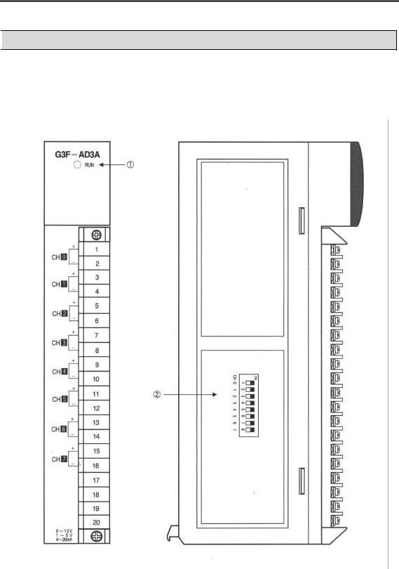
Chapter 2. SPECIFICATIONS
 2.3 Names of Parts and Functions
The names of parts and functions of the A/D conversion module are shown as below.
2.3.1 G3F-AD3A
2 - 4

Chapter 2. SPECIFICATIONS
2.3.2 G4F-AD3A
No |
|
Description |
|
←RUN LED
Indicates the operating status of the G3F-AD3A and G4F-AD3A.
−Selection switch of voltage/current 1)The switch status at voltage selection
On |
The switch locates off status. |
|
|
1 2 3 4 5 6 7 8 |
|
2)The switch statues at current selection
On


 The switch locates on status
1 2 3 4 5 6 7 8
2 - 5
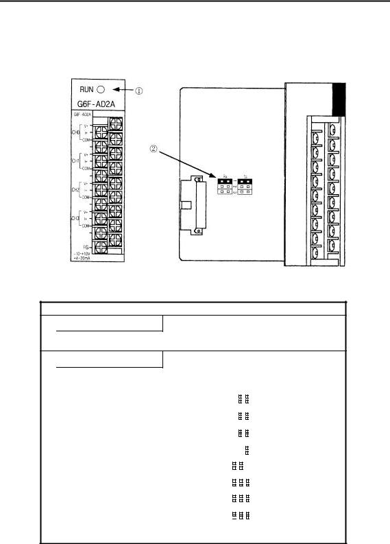
Chapter 2. SPECIFICATIONS
2.3.3G6F-AD2A
No |
Description |
←RUN LED
Indicates the operating status of the G6F-AD2A.
− Selection switch of voltage/current
|
Analog Input |
Input Range Selection Switch |
|||||||||
|
|
|
|
|
|
|
|
|
|
|
|
|
DC 1~5V |
J1 |
|
|
|
2 |
|
|
|
|
|
|
|
|
|
|
|
|
|
||||
|
|
|
|
|
|
|
|
||||
|
|
1 |
|
|
3 |
|
|||||
|
|
J2 |
|
|
|
|
|
|
|
|
|
|
|
|
|
|
|
|
|
|
|
|
|
|
|
|
|
|
|
|
|
|
|
|
|
Voltage |
DC 0~10V |
J1 |
|
|
|
|
|
|
|
|
|
|
1 |
|
2 |
|
3 |
|
|||||
|
|
J2 |
|
|
|
|
|
|
|
|
|
|
|
|
|
|
|
|
|
|
|
|
|
|
DC-10~10V |
J1 |
|
|
|
|
|
|
|
|
|
|
|
|
|
|
|
|
|
|
|
||
|
|
1 |
|
|
2 |
|
3 |
|
|||
|
|
J2 |
|
|
|
|
|
|
|
|
|
|
|
|
|
|
|
|
|
|
|
|
|
|
|
|
|
|
|
|
|
|
|
|
|
|
|
|
|
|
|
|
|
|
|
|
|
Current |
DC 4~20mA |
J1 |
|
|
|
|
|
|
|
|
|
|
|
|
|
|
|
|
|||||
|
1 |
|
|
2 |
|
3 |
|
||||
J2 |
|
|
|
|
|||||||
|
|
|
|
|
|
|
|
|
|
|
|
|
|
|
|
|
|
|
|
|
|
|
|
|
|
|
|
|
|
|
|
|
|
|
|
2 - 6
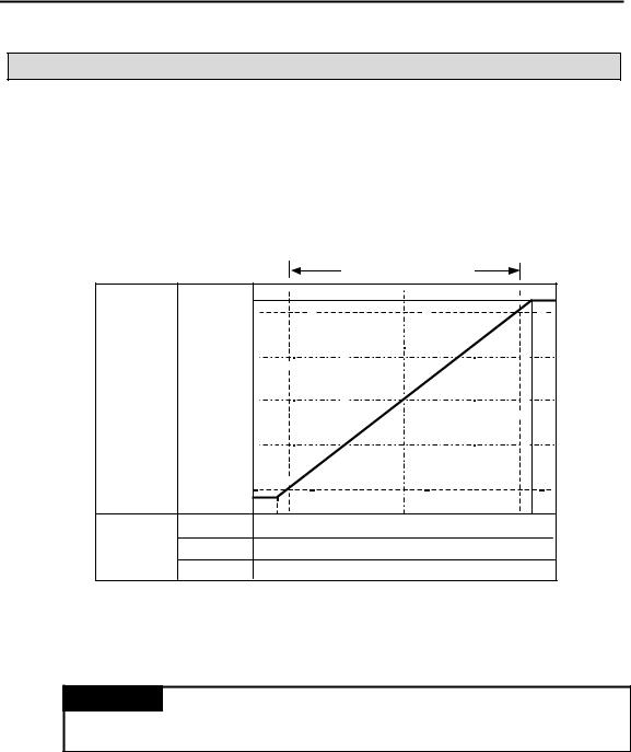
Chapter 2. SPECIFICATIONS
2.4 I/O Conversion Characteristics
Input / Output (hereafter I/O) conversion characteristics are expressed with the angle of the line between
analog input(voltage and current) and matched digital value.
I/O conversion characteristics of the G3F-AD3A, G4F-AD3A are expressed with Fig 2.1, and I/O conversion characteristics of the G6F-AD2A is expressed with Fig 2.2
The voltage or current input for a channel is selected by analog input selection switch and the value of
Offset / Gain can not be changed because it is fixed.
Practical analog input range
|
|
|
|
|
|
|
|
|
|
|
|
|
|
|
|
|
|
|
|
4047 |
|
|
|
|
|
|
|
|
|
|
|
|
|
|
|
|
|
|
|
|
|
|
|
|
|
|
|
|
|
|
|
|
||||
|
4000 |
|
|
|
|
|
|
|
|
|
|
|
|
|
|
|
|
|
|
|
|
|
|
|
|
|
|
|
|
|
|
|
|
|
|
||
|
|
|
|
|
|
|
|
|
|
|
|
|
|
|
|
|
|
|
Digital |
3000 |
|
|
|
|
|
|
|
|
|
|
|
|
|
|
|
|
|
|
|
|
|
|
|
|
|
|
|
|
|
|
|
|
|
|||
|
|
|
|
|
|
|
|
|
|
|
|
|
|
|
|
|
|
|
Output |
2000 |
|
|
|
|
|
|
|
|
|
|
|
|
|
|
|
|
|
|
|
|
|
|
|
|
|
|
|
|
|
|
|
|
|
|||
Value |
|
|
|
|
|
|
|
|
|
|
|
|
|
|
|
|
|
|
|
|
|
|
|
|
|
|
|
|
|
|
|
|
|
|
|
|
|
|
|
|
|
|
|
|
|
|
|
|
|
|
|
|
|
|
|
|
|
1000 |
|
|
|
|
|
|
|
|
|
|
|
|
|
|
|
|
|
|
|
|
|
|
|
|
|
|
|
|
|
|
|
|
|
|
||
|
|
|
|
|
|
|
|
|
|
|
|
|
|
|
|
|
|
|
|
|
0 |
|
|
|
|
|
|
|
|
-48 |
|
|
|
|
|
|
|
DC 0 ~ 10V |
-0.12V |
0V |
5V |
10V |
10.12V |
||
Analog |
|
|||||||
DC 1 |
~ 5V |
0.952V |
1V |
3V |
5V |
5.048 |
||
Input |
||||||||
DC 4 |
~ 20 |
3.808 |
|
|
20 20.192 |
|||
|
4 |
12 |
||||||
[Fig 2.1] I/O Conversion Characteristics
REMARK
1.The analog output value of over 4047 or –48 is fixed as 4047 or–48.
2.Keep the input voltage and current not to exceed +15V and 25mA.
2 - 7
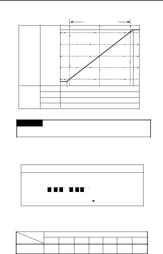
Chapter 2. SPECIFICATIONS
|
|
|
|
|
Practical analog input range |
|
|
|
2047 |
4047 |
|
|
|
|
|
|
2000 |
4000 |
|
|
|
|
|
|
1000 |
3000 |
|
|
|
|
|
Digital |
0 |
|
|
|
|
|
|
Output |
2000 |
|
|
|
|
|
|
Value |
|
|
|
|
|
|
|
|
-1000 |
1000 |
|
|
|
|
|
|
-2000 |
0 |
|
|
|
|
|
|
-2048 |
-48 |
|
|
|
|
|
|
DC 0 ~ 10V |
-0.12V |
0V |
5V |
10V |
10.12V |
|
Analog |
|
|
|||||
DC 1 ~ 5V |
|
0.952V |
1V |
3V |
5V |
5.048V |
|
Input |
|
||||||
|
|
|
|
|
|
||
|
DC-10 ~ 10V |
-10.24V |
-10V |
0V |
10V |
10.24V |
|
|
|
|
|||||
|
DC 4 ~ 20 |
3.808 4 |
12 |
20 20.192 |
|||
|
|
[Fig 2.1] |
I/O Conversion Characteristics |
|
|
||
REMARK
1.The analog output value of over 4047 or –48(2047 or –2048) is fixed as 4047 or –48(2047 or–2048).
2.Keep the input voltage and current not to exceed +15V and 25mA.
2.4.1Voltage Input Characteristics
1)G3F-AD3A, G4F-AD3A
For voltage input, the corresponding input selection switch of each channel should be set to "off".
Input selection switch
- Off : Voltage |
|
|
|
|
|
|
|
|
|
|
|
|
|
|
|
|
|
|
|
|
|
|
|
|
|
|
|
|
On |
|
|
|
|
|
|
|
|
|
|
|
|
|
|
|
|
|
|
|
|
|
|
|
|
|
|
|
|
|
|
|
|
|
|
|
|
|
|
|
|
|
|
|
|
|
|
(This switch is located |
|
|
||
|
|
|
|
|
|
|
|
|
|
|
|
|
|
|
|
|
|
|
|
|
|
|
|
|||
|
|
|
|
|
|
|
|
|
|
|
|
|
|
|
|
|
|
|
|
|
|
on the side of module) |
|
|
||
|
1 |
2 |
3 |
4 |
5 |
6 |
7 |
|
8 |
|
|
|
|
|
|
|
|
|||||||||
|
|
|
|
|
|
|
|
|
|
|
|
|
||||||||||||||
|
|
|
|
|
|
|
|
|
|
|
|
|
|
|
|
|
|
|
|
|
|
|
|
|
||
|
CH 0 |
1 |
|
2 |
3 |
4 |
5 |
6 7 |
|
|
|
|
|
Number of channel |
|
|||||||||||
|
|
|
|
|
|
|
|
|||||||||||||||||||
|
|
|
|
|
|
|
|
|
|
|
|
|
|
|
|
|
|
|
|
|
|
|
|
|
|
|
–The voltage input range is selected in program. Input selection switch has to be located at off.
(1)Voltage input range : DC 0~10V
Digital output value for input voltage is shown as follows.
|
|
|
|
Analog input voltage (V) |
|
|
|
|
-0.12 |
0 |
2.5 |
5 |
7.5 |
10 |
10.12 |
Digital output value |
-48 |
0 |
1000 |
2000 |
3000 |
4000 |
4047 |
2 - 8
Chapter 2. SPECIFICATIONS
(2)Voltage input range : DC 1~5V
Digital output value for input voltage is shown as follows.
|
|
|
|
Analog input voltage (V) |
|
|
|
|
0.952 |
1 |
2 |
3 |
4 |
5 |
5.048 |
Digital output value |
-48 |
0 |
1000 |
2000 |
3000 |
4000 |
4047 |
2) G6F-AD2A
For voltage input, the corresponding input is selected by selection switch and selected input voltage range is same through whole channels.
1)Voltage input range : DC 1~5V
Digital output value for input voltage is shown as follows.
|
|
Analog input voltage (V) |
|
|
|
Input range selection |
|||
|
|
|
|
|
switch |
||||
|
|
|
|
|
|
|
|||
0.952 |
1 |
2 |
3 |
4 |
5 |
5.048 |
J11 |
|
|
-48 |
0 |
1000 |
2000 |
3000 |
4000 |
4047 |
|
|
|
1 |
2 |
3 |
|||||||
Digital output value |
-2000 |
-1000 |
0 |
1000 |
2000 |
2047 |
J12 |
|
|
-2048 |
|
|
|
||||||
2)Voltage input range : DC 0 ~ 10V
Digital output value for input voltage is shown as follows.
|
|
Analog input voltage (V) |
|
|
|
Input range selection |
|||
|
|
|
|
|
switch |
|
|||
|
|
|
|
|
|
|
|
||
-0.12 |
0 |
2.5 |
5 |
7.5 |
10 |
10.12 |
J1 |
|
|
|
|
|
|
|
|
|
|
|
|
-48 |
0 |
1000 |
2000 |
3000 |
4000 |
4047 |
1 |
2 |
3 |
Digital output value |
-2000 |
-1000 |
0 |
1000 |
2000 |
2047 |
J2 |
|
|
-2048 |
|
|
|
||||||
3)Voltage input range : DC -10 ~ 10V
Digital output value for input voltage is shown as follows.
|
|
Analog input voltage (V) |
|
|
|
Input range selection |
|||
|
|
|
|
|
switch |
||||
|
|
|
|
|
|
|
|||
-10.24 |
-10 |
-5 |
0 |
5 |
10 |
10.24 |
J11 |
|
|
|
|
|
|
|
|
|
|
|
|
-48 |
0 |
1000 |
2000 |
3000 |
4000 |
4047 |
1 |
2 |
3 |
Digital output value |
-2000 |
-1000 |
0 |
1000 |
2000 |
2047 |
J12 |
|
|
-2048 |
|
|
|
||||||
2 - 9
Chapter 2. SPECIFICATIONS
2.4.2 Current Input Characteristics
1) G3F-AD3A, G4F-AD3A
For current input, the corresponding input selection switch of each channel should be set to "on".
Input selection switch
- On : Current
On
(This switch is located on the side of module)
1 |
2 |
3 |
4 |
5 |
6 |
7 |
8 |
|
|
|
|
|
|
|
|
|
|
|
|
|
|
|
|
|
|
CH 0 |
|
1 |
2 |
3 |
4 |
5 |
6 7 |
|
|
|
|
Number of channel |
|
|
|
|
|
||||||||
|
|
|
|
|
|
|
|
|
|
|
|
|
- Digital output value for input current is shown as follows.
|
|
|
|
Analog input current( ) |
|
|
|
|
3.808 |
4 |
8 |
12 |
16 |
20 |
20.192 |
Digital output value |
-48 |
0 |
1000 |
2000 |
3000 |
4000 |
4047 |
2)G6F-AD2A
Digital output value for input voltage is shown as follows.
|
|
Analog input current (mA) |
|
|
|
Input range selection |
|||
|
|
|
|
|
switch |
|
|||
|
|
|
|
|
|
|
|
||
3.808 |
4 |
8 |
12 |
16 |
20 |
20.192 |
11J |
|
|
|
|
|
|
|
|
|
|
|
|
-48 |
0 |
1000 |
2000 |
3000 |
4000 |
4047 |
1 |
2 |
3 |
|
|
|
|||||||
Digital output value |
-2000 |
-1000 |
0 |
1000 |
2000 |
2047 |
12J |
|
|
-2048 |
|
|
|
||||||
It has to be connected between V and I terminal to select current.
2 - 10
Chapter 2. SPECIFICATIONS
2.4.3 Simultaneous Voltage and Current Input Characteristics
1)G3F-AD3A, G4F-AD3A
For simultaneous voltage and current input, the input conversion switch of each channel is set to corresponding
voltage and current range. |
|
Ex) Voltage input range: 0 to 3 |
Current input range: 4 to 7 |
Input selection switch
- On : Current
- Off : Voltage On
|
|
|
|
|
|
|
|
|
|
|
|
|
|
|
|
|
|
|
|
|
|
|
|
|
|
|
|
|
|
|
|
|
|
|
|
|
|
|
|
|
|
|
|
|
|
|
( ) |
||||
|
|
|
|
|
|
|
|
|
|
|
|
|
|
|
|
|
|
|
|||||||
|
|
|
|
|
|
|
|
|
|
|
|
|
|
|
|
|
|
|
|
|
|
|
|
|
|
|
1 |
2 |
3 |
4 |
5 |
6 |
7 |
8 |
|
|
|
|
|
|
|
|
|
|
|
||||||
CH 0 1 2 3 |
4 5 6 7 |
|
|
|
|
|
|
|
|
||||||||||||||||
|
|
|
|
|
|
|
|||||||||||||||||||
|
|
|
|
|
|
|
|
|
|
|
|
|
|
|
|
|
|
|
|
|
|
|
|
|
|
- Digital output value for analog input is shown as follows..
|
|
|
|
|
Analog input |
|
|
|
|
Voltage |
0~10V |
-0.12 |
0 |
2.5 |
5 |
7.5 |
10 |
10.12 |
|
(V) |
1~ 5V |
0.952 |
1 |
2 |
3 |
4 |
5 |
5.048 |
|
|
|||||||||
Current |
4 ~ 20 mA |
3.808 |
4 |
8 |
12 |
16 |
20 |
20.192 |
|
(mA) |
|||||||||
|
|
|
|
|
|
|
|
||
Digital output value |
-48 |
0 |
1000 |
2000 |
3000 |
4000 |
4047 |
||
2) G6F-AD2A
For simultaneous use of voltage and current input, the available input voltage rage is 0 ~ 5VDC only.
Digital output value for analog input is shown as follows..
|
|
|
|
Analog input |
|
|
|
|
Voltage DC1~ 5V |
0.952 |
1 |
2 |
3 |
4 |
5 |
5.048 |
|
Current DC4 ~ 20mA |
3.808 |
4 |
8 |
12 |
16 |
20 |
20.192 |
|
Digital output value |
-48 |
0 |
1000 |
2000 |
3000 |
4000 |
4047 |
|
-2048 |
-2000 |
-1000 |
0 |
1000 |
2000 |
2047 |
||
|
||||||||
Ex) channel for voltage : 0, |
channel for current : 1 |
|
|
|
|
|
||
Input Rage Selection Switch |
|
|
|
|
|
|
|
Wiring Example |
|
|
|
|
|
||||||||||||||||
|
|
|
|
|
|
|
|
|
|
|
|
|
|
|
|
|
|
|
|
||||||||||
|
|
|
|
|
|
|
|
|
|
|
Voltage Input(Channel “0”) |
|
|
|
|
|
Current Input(Channel ”1”) |
||||||||||||
J1 |
|
|
|
|
|
|
|
|
|
|
|
|
|
|
|
|
|
|
|
|
|
|
+ |
|
|
|
|
|
|
|
|
|
|
|
|
|
|
|
|
|
|
|
|
|
|
|
|
|
|
|
|
|
|
|
|
|
|||
|
|
|
|
|
|
|
|
|
|
|
|
|
|
|
|
|
|
|
|
|
|
|
|
|
|
|
|||
|
|
|
|
|
|
|
|
|
|
|
+ |
|
V+ |
|
|
|
|
|
|
|
|
|
V+ |
|
|
|
|||
|
|
|
|
|
|
|
|
|
|
|
|
|
|
|
|
|
|
|
|
|
|
|
|
|
|
|
|
|
|
|
|
|
|
|
|
|
|
|
|
|
|
|
|
|
|
|
|
|
|
|
|
|
|
|
|
|
|
|
|
|
|
|
|
|
|
|
|
|
|
|
|
|
|
|
|
|
|
|
|
|
|
|
|
|
|
|
|
|
|
|
|
|
|
|
|
|
|
|
|
|
|
|
|
|
|
|
|
|
|
|
|
|
|
|
|
|
|
|
|
|
1 |
|
2 |
|
|
3 |
|
|
|
Analog Input |
|
I+ |
|
|
|
|
|
Analog Input |
|
I+ |
|
|
|||||||
|
|
|
|
|
|
|
|
|
|
|
|
||||||||||||||||||
|
|
|
|
|
|
|
|
|
|
|
|
|
|
|
|
|
|
|
|
|
|
|
|
|
|
|
|
|
|
|
|
|
|
|
|
|
|
|
|
|
|
|
|
|
|
|
|
|
|
|
|
|
|
|
COM |
|
|
||
J2 |
|
|
|
|
|
|
|
|
|
|
|
|
|
COM |
|
|
|
||||||||||||
|
|
|
|
|
|
|
|
|
|
|
|
|
|
|
|
|
|
|
|
|
|
|
|
|
|
|
|
|
|
|
|
|
|
|
|
|
|
|
|
|
|
|
|
|
|
|
|
|
|
|
|
|
|
|
|
|
|
|
|
|
|
|
|
|
|
|
|
|
|
|
|
|
|
|
|
|
|
|
|
|
|
|
|
|
|
|
|
|
|
2 - 11
Chapter 2. SPECIFICATIONS
2.4.4 Analog input and Digital output characteristics
1)G3F-AD3A, G4F-AD3A
|
|
|
|
|
|
|
|
|
|
|
|
|
|
|
|
|
|
|
|
|
|
|
|
|
|
|
|
|
|
|
|
|
|
|
|
|
|
|
|
|
|
|
|
|
|
|
|
|
|
|
|
|
|
|
|
|
|
|
|
|
|
|
|
|
|
|
|
|
|
|
|
|
|
|
|
|
|
|
|
|
|
|
|
|
2009 |
|
|
|
|
|
|
|
|
|
|
|
|
|
|
|
|
|
|
|
|
|
|
|
|
|
|
|
|
|
|
|
|
|
|
|
|
|
|
|
|
|
|
|
|
|
|
|
|
|
|
|
|
|
|
|
|
|
|
|
|
|
|
|
|
|
|
|
|
|
|
||||
|
|
|
|
|
|
|
|
|
|
|
|
|
|
|
|
|
|
|
|
|
|
|
|
|
|
|
|
|
|
|
|
|
|
|
|
|
|||
|
|
|
|
|
2008 |
|
|
|
|
|
|
|
|
|
|
|
|
|
|
|
|
|
|
|
|
|
|
|
|
|
|
|
|
|
|
|
|
|
|
|
|
|
|
|
|
|
|
|
|
|
|
|
|
|
|
|
|
|
|
|
|
|
|
|
|
|
|
|
|
|
|
|
|
|
|
||||
|
|
|
|
|
|
|
|
|
|
|
|
|
|
|
|
|
|
|
|
|
|
|
|
|
|
|
|
|
|
|
|
|
|
|
|
|
|
||
|
|
|
|
|
2007 |
|
|
|
|
|
|
|
|
|
|
|
|
|
|
|
|
|
|
|
|
|
|
|
|
|
|
|
|
|
|
|
|
||
|
|
|
|
|
|
|
|
|
|
|
|
|
|
|
|
|
|
|
|
|
|
|
|
|
|
|
|
|
|
|
|
|
|
||||||
|
|
|
|
|
|
|
|
|
|
|
|
|
|
|
|
|
|
|
|
|
|
|
|
|
|
|
|
|
|
|
|
|
|
|
|
|
|||
|
Digital output value |
2006 |
|
|
|
|
|
|
|
|
|
|
|
|
|
|
|
|
|
|
|
|
|
|
|
|
|
|
|
|
|
|
|||||||
|
|
|
|
|
|
|
|
|
|
|
|
|
|
|
|
|
|
|
|
|
|
|
|
|
|
|
|
|
|
|
|
|
|
|
|||||
|
|
|
|
|
|
|
|
|
|
|
|
|
|
|
|
|
|
|
|
|
|
|
|
|
|
|
|
|
|
|
|
|
|||||||
|
|
|
|
|
|
|
|
|
|
|
|
|
|
|
|
|
|
|
|
|
|
|
|
|
|
|
|
|
|
|
|
|
|
|
|
|
|||
|
|
2005 |
|
|
|
|
|
|
|
|
|
|
|
|
|
|
|
|
|
|
|
|
|
|
|
|
|
|
|
|
|
|
|
|
|
||||
|
|
|
|
|
|
|
|
|
|
|
|
|
|
|
|
|
|
|
|
|
|
|
|
|
|
|
|
|
|
|
|
|
|
|
|
|
|
||
|
|
|
|
|
|
|
|
|
|
|
|
|
|
|
|
|
|
|
|
|
|
|
|
|
|
|
|
|
|
|
|
|
|
|
|
|
|||
|
|
|
|
|
2004 |
|
|
|
|
|
|
|
|
|
|
|
|
|
|
|
|
|
|
|
|
|
|
|
|
|
|
|
|
|
|
|
|
|
|
|
|
|
|
|
|
|
|
|
|
|
|
|
|
|
|
|
|
|
|
|
|
|
|
|
|
|
|
|
|
|
|
|
|
|
|
||||
|
|
|
|
|
2003 |
|
|
|
|
|
|
|
|
|
|
|
|
|
|
|
|
|
|
|
|
|
|
|
|
|
|
|
|
|
|
|
|
|
|
|
|
|
|
|
|
|
|
|
|
|
|
|
|
|
|
|
|
|
|
|
|
|
|
|
|
|
|
|
|
|
|
|
|
|
|
||||
|
|
|
|
|
2002 |
|
|
|
|
|
|
|
|
|
|
|
|
|
|
|
|
|
|
|
|
|
|
|
|
|
|
|
|
|
|
|
|
|
|
|
|
|
|
|
|
|
|
|
|
|
|
|
|
|
|
|
|
|
|
|
|
|
|
|
|
|
|
|
|
|
|
|
|
|
|
||||
|
|
|
|
|
|
|
|
|
|
|
|
|
|
|
|
|
|
|
|
|
|
|
|
|
|
|
|
|
|
|
|
|
|
|
|
|
|
|
|
|
|
|
|
2001 |
|
|
|
|
|
|
|
|
|
|
|
|
|
|
|
|
|
|
|
|
|
|
|
|
|
|
|
|
|
|
|
|
|||
|
|
|
|
|
2000 |
|
|
|
|
|
|
|
|
|
|
|
|
|
|
|
|
|
|
|
|
|
|
|
|
|
|
|
|
|
|
|
|||
|
|
|
|
|
|
|
|
|
|
|
|
|
|
|
|
|
|
|
|
|
|
|
|
|
|
|
|
|
|
|
|
|
|||||||
|
|
|
|
|
|
|
|
|
|
|
|
|
|
|
|
|
|
|
|
|
|
|
|
|
|
|
|
|
|
|
|
|
|
|
|
|
|
|
|
|
|
|
|
|
|
|
|
|
|
|
|
|
|
|
|
|
|
|
|
|
|
|
|
|
|
|
|
|
|
|
|
|
|
|
|
|
|
|
|
|
No |
Input |
|
Digital |
Resolution |
|
|
|
|
|
|
|
|
|
Analog input value |
|
|
|
|
|
|
|
|
|
|
|
|
|
|
|
|
|
|||||||
|
|
output |
|
|
|
|
|
|
|
|
|
|
|
|
|
|
|
|
|
|
|
|
|
|
|
|
|
|
|||||||||||
|
range |
|
|
|
|
|
|
|
|
|
|
|
|
|
|
|
|
|
|
|
|
|
|
|
|
|
|
|
|||||||||||
|
|
|
value |
|
|
|
|
|
|
|
|
|
|
|
|
|
|
|
|
|
|
|
|
|
|
|
|
|
|
|
|
|
|
|
|
|
|
||
|
|
|
|
|
|
|
|
|
|
|
|
|
|
|
|
|
|
|
|
|
|
|
|
|
|
|
|
|
|
|
|
|
|
|
|
|
|
||
|
|
|
|
|
|
|
|
|
|
|
|
|
|
|
|
|
|
|
|
|
|
|
|
|
|
|
|
|
|
|
|
|
|
|
|
|
|
|
|
|
|
DC 0~10V |
|
|
|
|
|
2.5 mV |
|
5.000 |
|
|
|
|
5.0025 |
|
|
|
5.005 |
|
|
|
|
|
5.0075 |
|
|
|
|
|
|||||||||
|
|
|
|
|
|
|
|
~ |
|
|
|
|
~ |
|
|
|
|
|
~ |
|
|
|
|
|
~ |
|
|
|
|
|
|
|
|||||||
|
|
|
|
|
|
|
|
|
|
|
5.0025 |
|
|
|
|
5.005 |
|
|
|
|
5.0075 |
|
|
|
|
|
5.010 |
|
|
|
|
|
|
||||||
|
|
|
|
0 |
|
|
|
|
|
|
|
|
|
|
|
|
|
|
|
|
|
|
|
|
|
|
|
|
|
|
|
|
|
|
|
|
|
|
|
|
|
|
|
|
|
|
|
3.000 |
|
3.001 |
|
3.002 |
|
3.003 |
|
3.004 |
|
3.005 |
|
|
3.006 |
|
3.007 |
|
3.008 |
|
|
3.009 |
|
|
|||||||||
|
|
DC 1~5V |
|
~ |
|
|
|
1mV |
~ |
|
~ |
|
~ |
|
~ |
|
~ |
|
~ |
|
|
~ |
|
~ |
|
|
~ |
|
|
|
~ |
|
|
|
|||||
|
|
|
|
4000 |
|
|
|
|
3.001 |
|
3.002 |
|
3.003 |
|
3.004 |
|
3.005 |
|
3.006 |
|
|
3.007 |
|
3.008 |
|
3.009 |
|
|
3.010 |
|
|
||||||||
|
|
|
|
|
|
|
|
|
|
|
|
|
|
|
|
|
|
|
|
|
|
|
|
|
|
|
|
|
|
|
|
|
|
|
|
|
|
|
|
|
|
DC 4~20 |
|
|
|
|
|
|
|
12.000 |
|
12.004 |
|
12.008 |
|
12.012 |
|
12.016 |
|
12.020 |
|
|
12.024 |
|
12.028 |
|
12.032 |
|
|
12.036 |
|
|
|||||||
|
|
|
|
|
|
|
4 |
~ |
|
~ |
|
~ |
|
~ |
|
~ |
|
~ |
|
|
~ |
|
~ |
|
|
~ |
|
|
|
~ |
|
|
|
||||||
|
|
|
|
|
|
|
|
|
|
|
|
|
|
|
|
|
|
|
|
|
|
|
|||||||||||||||||
|
|
|
|
|
|
|
|
|
12.004 |
|
12.008 |
|
12.012 |
|
12.016 |
|
12.020 |
|
12.024 |
|
|
12.028 |
|
12.032 |
|
12.036 |
|
|
12.040 |
|
|
||||||||
|
|
|
|
|
|
|
|
|
|
|
|
|
|
|
|
|
|
|
|
|
|
|
|||||||||||||||||
|
|
|
|
|
|
|
|
|
|
|
|
|
|
|
|
|
|
|
|
|
|
|
|
|
|
|
|
|
|
|
|
|
|
|
|
|
|
|
|
|
|
|
|
|
|
|
|
|
|
|
|
|
|
|
|
|
|
|
|
|
|
|
|
|
|
|
|
|
|
|
|
|
|
|
|
|
|
|
|
|
|
|
|
|
|
|
|
|
|
|
|
Analog input and Digital output |
|
|
|
|
|
|
|
|
|
|
|
|
|
|
|
|
|
|
|
||||||||
|
2) G6F-AD2A |
|
|
|
|
|
|
|
|
|
|
|
|
|
|
|
|
|
|
|
|
|
|
|
|
|
|
|
|
|
|
|
|
|
|
|
|
||
|
|
|
|
|
|
|
|
|
|
|
|
|
|
|
|
|
|
|
|
|
|
|
|
|
|
|
|
|
|
|
|
|
|
|
|
|
|
|
|
|
|
|
|
2009 |
|
|
|
|
|
|
|
|
|
|
|
|
|
|
|
|
|
|
|
|
|
|
|
|
|
|
|
|
|
|
|
|
|||
|
|
|
|
|
|
|
|
|
|
|
|
|
|
|
|
|
|
|
|
|
|
|
|
|
|
|
|
|
|
|
|
|
|
|
|
||||
|
|
|
|
|
|
|
|
|
|
|
|
|
|
|
|
|
|
|
|
|
|
|
|
|
|
|
|
|
|
|
|
|
|
|
|
|
|||
|
|
|
|
|
2008 |
|
|
|
|
|
|
|
|
|
|
|
|
|
|
|
|
|
|
|
|
|
|
|
|
|
|
|
|
|
|
|
|
|
|
|
|
|
|
|
|
|
|
|
|
|
|
|
|
|
|
|
|
|
|
|
|
|
|
|
|
|
|
|
|
|
|
|
|
|
|
||||
|
|
|
|
|
|
|
|
|
|
|
|
|
|
|
|
|
|
|
|
|
|
|
|
|
|
|
|
|
|
|
|
|
|
|
|
|
|
||
|
|
|
|
2007 |
|
|
|
|
|
|
|
|
|
|
|
|
|
|
|
|
|
|
|
|
|
|
|
|
|
|
|
|
|
|
|
||||
|
|
|
|
|
|
|
|
|
|
|
|
|
|
|
|
|
|
|
|
|
|
|
|
|
|
|
|
|
|
|
|
|
|
||||||
|
|
|
|
|
|
|
|
|
|
|
|
|
|
|
|
|
|
|
|
|
|
|
|
|
|
|
|
|
|
|
|
|
|
|
|||||
|
Digital output value |
|
2006 |
|
|
|
|
|
|
|
|
|
|
|
|
|
|
|
|
|
|
|
|
|
|
|
|
|
|
|
|
|
|
|
|
|
|||
|
|
|
|
|
|
|
|
|
|
|
|
|
|
|
|
|
|
|
|
|
|
|
|
|
|
|
|
|
|
|
|
||||||||
|
|
|
|
|
|
|
|
|
|
|
|
|
|
|
|
|
|
|
|
|
|
|
|
|
|
|
|
|
|
|
|||||||||
|
|
2005 |
|
|
|
|
|
|
|
|
|
|
|
|
|
|
|
|
|
|
|
|
|
|
|
|
|
|
|||||||||||
|
|
|
|
|
|
|
|
|
|
|
|
|
|
|
|
|
|
|
|
|
|
|
|
|
|
|
|
|
|
|
|
|
|
|
|
|
|
||
|
|
|
|
|
|
|
|
|
|
|
|
|
|
|
|
|
|
|
|
|
|
|
|
|
|
|
|
|
|
|
|
|
|
|
|
|
|
|
|
|
|
|
|
2004 |
|
|
|
|
|
|
|
|
|
|
|
|
|
|
|
|
|
|
|
|
|
|
|
|
|
|
|
|
|
|
|
|
|||
|
|
|
|
|
|
|
|
|
|
|
|
|
|
|
|
|
|
|
|
|
|
|
|
|
|
|
|
|
|
|
|
|
|
|
|
||||
|
|
|
|
|
2003 |
|
|
|
|
|
|
|
|
|
|
|
|
|
|
|
|
|
|
|
|
|
|
|
|
|
|
|
|
|
|
|
|
|
|
|
|
|
|
|
|
|
|
|
|
|
|
|
|
|
|
|
|
|
|
|
|
|
|
|
|
|
|
|
|
|
|
|
|
|
|
||||
|
|
|
|
|
2002 |
|
|
|
|
|
|
|
|
|
|
|
|
|
|
|
|
|
|
|
|
|
|
|
|
|
|
|
|
|
|
|
|
|
|
|
|
|
|
|
|
|
|
|
|
|
|
|
|
|
|
|
|
|
|
|
|
|
|
|
|
|
|
|
|
|
|
|
|
|
|
||||
|
|
|
|
|
|
|
|
|
|
|
|
|
|
|
|
|
|
|
|
|
|
|
|
|
|
|
|
|
|
|
|
|
|
|
|
|
|
|
|
|
|
|
|
2001 |
|
|
|
|
|
|
|
|
|
|
|
|
|
|
|
|
|
|
|
|
|
|
|
|
|
|
|
|
|
|
|
|
|||
|
|
|
|
|
|
|
|
|
|
|
|
|
|
|
|
|
|
|
|
|
|
|
|
|
|
|
|
|
|
|
|
|
|
|
|
||||
|
|
|
|
|
2000 |
|
|
|
|
|
|
|
|
|
|
|
|
|
|
|
|
|
|
|
|
|
|
|
|
|
|
|
|
|
|
|
|
|
|
|
|
|
|
|
|
|
|
|
|
|
|
|
|
|
|
|
|
|
|
|
|
|
|
|
|
|
|
|
|
|
|
|
|
|
|||||
|
|
|
|
|
|
|
|
|
|
|
|
|
|
|
|
|
|
|
|
|
|
|
|
|
|
|
|
|
|
|
|
|
|
|
|
||||
|
|
|
|
|
|
|
|
|
|
|
|
|
|
|
|
|
|
|
|
|
|
|
|
|
|
|
|
|
|
|
|
|
|
|
|
|
|
|
|
|
No |
Input range |
Digital |
Resolution |
|
|
|
|
|
|
|
|
|
Analog input value |
|
|
|
|
|
|
|
|
|
|
|
|
|
|
|
|
|
||||||||
|
output |
|
|
|
|
|
|
|
|
|
|
|
|
|
|
|
|
|
|
|
|
|
|
|
|
|
|
||||||||||||
|
|
|
|
value |
|
|
|
|
|
|
|
|
|
|
|
|
|
|
|
|
|
|
|
|
|
|
|
|
|
|
|
|
|
|
|
|
|
|
|
|
|
|
|
|
|
|
|
|
|
|
|
|
|
|
|
|
|
|
|
|
|
|
|
|
|
|
|
|
|
|
|
|
|
|
|
|
|||
|
|
DC-10~10V |
|
|
|
|
5mV |
|
|
|
|
0.000 |
|
|
|
|
|
|
|
|
|
|
0.005 |
|
|
|
|
|
|
|
|
|
|
|
|||||
|
|
|
|
|
|
|
|
|
|
~ |
|
|
|
|
|
|
|
|
|
|
~ |
|
|
|
|
|
|
|
|
|
|
|
|
||||||
|
|
|
|
|
|
|
|
|
|
|
|
|
|
0.005 |
|
|
|
|
|
|
|
|
|
|
0.010 |
|
|
|
|
|
|
|
|
|
|
|
|||
|
|
|
|
0 ~ |
|
|
|
|
|
|
|
|
|
|
|
|
|
|
|
|
|
|
|
|
|
|
|
|
|
|
|
||||||||
|
|
|
|
|
|
|
|
|
5.000 |
|
|
|
|
5.0025 |
|
|
|
5.005 |
|
|
|
|
|
5.0075 |
|
|
|
|
|
||||||||||
|
|
DC 0~10V |
4000 |
|
|
2.5 mV |
|
~ |
|
|
|
|
~ |
|
|
|
|
|
~ |
|
|
|
|
|
~ |
|
|
|
|
|
|
|
|||||||
|
|
|
|
or |
|
|
|
|
|
5.0025 |
|
|
|
|
5.005 |
|
|
|
|
5.0075 |
|
|
|
|
|
5.010 |
|
|
|
|
|
|
|||||||
|
|
|
|
|
|
|
|
|
|
|
|
|
|
|
|
|
|
|
|
|
|
|
|
|
|
|
|
|
|
|
|
|
|
|
|
|
|
||
|
|
|
|
-2048 |
|
|
|
|
3.000 |
|
3.001 |
|
3.002 |
|
3.003 |
|
3.004 |
|
3.005 |
|
|
3.006 |
|
3.007 |
|
3.008 |
|
|
3.009 |
|
|
||||||||
|
|
DC 1~5V |
~ |
|
|
1mV |
~ |
|
~ |
|
~ |
|
~ |
|
~ |
|
~ |
|
|
~ |
|
~ |
|
|
~ |
|
|
|
~ |
|
|
|
|||||||
|
|
|
|
2047 |
|
|
|
|
3.001 |
|
3.002 |
|
3.003 |
|
3.004 |
|
3.005 |
|
3.006 |
|
|
3.007 |
|
3.008 |
|
3.009 |
|
|
3.010 |
|
|
||||||||
|
|
|
|
|
|
|
|
|
|
|
|
|
|
|
|
|
|
|
|
|
|
|
|
|
|
|
|
|
|
|
|
|
|
|
|
|
|
||
|
|
|
|
|
|
|
|
|
|
12.000 |
|
12.004 |
|
12.008 |
|
12.012 |
|
12.016 |
|
12.020 |
|
|
12.024 |
|
12.028 |
|
12.032 |
|
|
12.036 |
|
|
|||||||
|
|
DC 4~20 |
|
|
|
|
4 |
~ |
|
~ |
|
~ |
|
~ |
|
~ |
|
~ |
|
|
~ |
|
~ |
|
|
~ |
|
|
|
~ |
|
|
|
||||||
|
|
|
|
|
|
|
|
|
|
12.004 |
|
12.008 |
|
12.012 |
|
12.016 |
|
12.020 |
|
12.024 |
|
|
12.028 |
|
12.032 |
|
12.036 |
|
|
12.040 |
|
|
|||||||
|
|
|
|
|
|
|
|
|
|
|
|
|
|
|
|
|
|
|
|
|
|
|
|
|
|
|
|
|
|
|
|
|
|
|
|
|
|
|
|
|
|
|
|
|
|
|
|
|
|
|
|
|
|
|
|
|
|
|
|
|
|
|
|
|
|
|
|
|
|
|
|
|
|
|
|
|
|
|
|
Analog input and digital output value
2 - 12

Chapter 2. SPECIFICATIONS
 2.5 Processing specifications
2.5.1 Sampling processing A/D conversion system
The analog values input to the channels designated for sampling processing by the CPU are converted to digital output values one by one and the digital output values are stored in the buffer memory.
As the A/D module scans each channel, the value appearing at the instant is written to the buffer memory as a digital value. The timing of this sampling depends on the number of channels used, and may be found from the following expression.
Process time = Number of channels used × Maximum conversion time (5 ms)
The process time when 4 channels is used, for example, will be 20 msec = 4 × 5 ms
2.5.2 Averaging processing A/D conversion system
The A/D module makes the A/D conversion for any channels to which averaging processing has been specified from the CPU. Using a pres et count, an average is calculated (excluding the maximum value and the minimum value) and stored to the buffer memory. The preset count can be set as 2 to 255 times.
The time in which the average value by this processing is stored in the buffer memory varies with the number of channels used.
Processing time = Count setting × No. of channels × 5ms (Max conversion time)
The processing time when count value is 50 and 4 channels are used, for example, will be 50 × 4 ×5ms = 1000ms.
2 - 13
 Loading...