


Lattice Semiconductor Corporation M4LV-96-48-7VC, M4LV-96-48-18VI, M4LV-96-48-15VC, M4LV-96-48-14VI, M4LV-96-48-12VI Datasheet
...MACH 4 CPLD Family
High Performance E2CMOS®
In-System Programmable Logic
FEATURES
High-performance, E2CMOS 3.3-V & 5-V CPLD families
Flexible architecture for rapid logic designs
—Excellent First-Time-FitTM and refit feature
—SpeedLockingTM performance for guaranteed fixed timing
—Central, input and output switch matrices for 100% routability and 100% pin-out retention
High speed
—7.5ns tPD Commercial and 10ns tPD Industrial
—111.1MHz fCNT
32 to 256 macrocells; 32 to 384 registers
44 to 256 pins in PLCC, PQFP, TQFP and BGA packages
Flexible architecture for a wide range of design styles
—D/T registers and latches
—Synchronous or asynchronous mode
—Dedicated input registers
—Programmable polarity
—Reset/ preset swapping
Advanced capabilities for easy system integration
—3.3-V & 5-V JEDEC-compliant operations
—JTAG (IEEE 1149.1) compliant for boundary scan testing
—3.3-V & 5-V JTAG in-system programming
—PCI compliant (-7/-10/-12 speed grades)
—Safe for mixed supply voltage system designs
—Bus-FriendlyTM inputs and I/Os
—Programmable security bit
—Individual output slew rate control
Advanced E2CMOS process provides high-performance, cost-effective solutions
Supported by ispDesignEXPERTTM software for rapid logic development
—Supports HDL design methodologies with results optimized for MACH 4
—Flexibility to adapt to user requirements
—Software partnerships that ensure customer success
Lattice and third-party hardware programming support
—LatticePROTM software for in-system programmability support on PCs and automated test equipment
—Programming support on all major programmers including Data I/O, BP Microsystems, Advin, and System General
Publication# 17466 |
Rev: M |
Amendment/0 |
Issue Date: March 2000 |

Table 1. MACH 4 Device Features1, 2
|
M4-32/32 |
M4-64/32 |
M4-96/48 |
M4-128/64 |
M4-128N/64 |
M4-192/96 |
M4-256/128 |
Feature |
M4LV-32/32 |
M4LV-64/32 |
M4LV-96/48 |
M4LV-128/64 |
M4LV-128N/64 |
M4LV-192/96 |
M4LV-256/128 |
|
|
|
|
|
|
|
|
Macrocells |
32 |
64 |
96 |
128 |
128 |
192 |
256 |
|
|
|
|
|
|
|
|
Maximum User I/O Pins |
32 |
32 |
48 |
64 |
64 |
96 |
128 |
|
|
|
|
|
|
|
|
tPD (ns) |
7.5 |
7.5 |
7.5 |
7.5 |
7.5 |
7.5 |
7.5 |
fCNT (MHz) |
111 |
111 |
111 |
111 |
111 |
111 |
111 |
tCOS (ns) |
5.5 |
5.5 |
5.5 |
5.5 |
5.5 |
5.5 |
5.5 |
tSS (ns) |
5.5 |
5.5 |
5.5 |
5.5 |
5.5 |
5.5 |
5.5 |
Static Power (mA) |
25 |
25 |
50 |
70 |
70 |
85 |
100 |
|
|
|
|
|
|
|
|
JTAG Compliant |
Yes |
Yes |
Yes |
Yes |
No |
Yes |
Yes |
|
|
|
|
|
|
|
|
PCI Compliant |
Yes |
Yes |
Yes |
Yes |
Yes |
Yes |
Yes |
|
|
|
|
|
|
|
|
Notes:
1.For information on the M4-96/96 device, please refer to the M4-96/96 data sheet at www.latticesemi.com.
2.“M4-xxx” is for 5-V devices. “M4LV-xxx” is for 3.3-V devices.
2 |
MACH 4 Family |

GENERAL DESCRIPTION
The MACH® 4 family from Lattice offers an exceptionally flexible architecture and delivers a superior Complex Programmable Logic Device (CPLD) solution of easy-to-use silicon products and software tools. The overall benefits for users are a guaranteed and predictable CPLD solution, faster time-to-market, greater flexibility and lower cost. The MACH 4 devices offer densities ranging from 32 to 256 macrocells with 100% utilization and 100% pin-out retention. The MACH 4 family offer 5-V (M4-xxx) and 3.3-V (M4LV-xxx) operation.
MACH 4 products are 5-V or 3.3-V in-system programmable through the JTAG (IEEE Std. 1149.1) interface. JTAG boundary scan testing also allows product testability on automated test equipment for device connectivity.
All MACH 4 family members deliver First-Time-Fit and easy system integration with pin-out retention after any design change and refit. For both 3.3-V and 5-V operation, MACH 4 products
can deliver guaranteed fixed timing as fast as 7.5 ns tPD and 111 MHz fCNT through the SpeedLocking feature when using up to 20 product terms per output (Table 2).
Table 2. MACH 4 Speed Grades
|
|
|
|
|
Speed Grade1 |
|
|
|
Device |
|
-7 |
-10 |
-12 |
|
-14 |
-15 |
-18 |
|
|
|
|
|
|
|
|
|
M4-32/32 |
|
C |
C, I |
C, I |
|
I |
C |
I |
M4LV-32/32 |
|
|
||||||
|
|
|
|
|
|
|
|
|
|
|
|
|
|
|
|
|
|
M4-64/32 |
|
C |
C, I |
C, I |
|
I |
C |
I |
M4LV-64/32 |
|
|
||||||
|
|
|
|
|
|
|
|
|
|
|
|
|
|
|
|
|
|
M4-96/48 |
|
C |
C, I |
C, I |
|
I |
C |
I |
M4LV-96/48 |
|
|
||||||
|
|
|
|
|
|
|
|
|
|
|
|
|
|
|
|
|
|
M4-128/64 |
|
C |
C, I |
C, I |
|
I |
C |
I |
M4LV-128/64 |
|
|
||||||
|
|
|
|
|
|
|
|
|
|
|
|
|
|
|
|
|
|
M4-128N/64 |
|
C |
C, I |
C, I |
|
I |
C |
I |
M4LV-128N/64 |
|
|
||||||
|
|
|
|
|
|
|
|
|
|
|
|
|
|
|
|
|
|
M4-192/96 |
|
C |
C, I |
C, I |
|
I |
C |
I |
M4LV-192/96 |
|
|
||||||
|
|
|
|
|
|
|
|
|
|
|
|
|
|
|
|
|
|
M4-256/128 |
|
C |
C, I |
C, I |
|
I |
C |
I |
M4LV-256/128 |
|
|
||||||
|
|
|
|
|
|
|
|
|
|
|
|
|
|
|
|
|
|
Note: |
|
|
|
|
|
|
|
|
1. C = Commercial, |
I = Industrial |
|
|
|
|
|
|
|
The MACH 4 family offers numerous density-I/O combinations in Thin Quad Flat Pack (TQFP), Plastic Quad Flat Pack (PQFP), Plastic Leaded Chip Carrier (PLCC), and Ball Grid Array (BGA) packages ranging from 44 to 256 pins (Table 3). It also offers I/O safety features for mixedvoltage designs so that the 3.3-V devices can accept 5-V inputs, and 5-V devices do not overdrive 3.3-V inputs. Additional features include Bus-Friendly inputs and I/Os, a programmable powerdown mode for extra power savings and individual output slew rate control for the highest speed transition or for the lowest noise transition.
MACH 4 Family |
3 |

Table 3. MACH 4 Package and I/O Options (Number of I/Os and dedicated inputs in Table)
|
M4-32/32 |
M4-64/32 |
M4-96/48 |
M4-128/64 |
M4-128N/64 |
M4-192/96 |
M4-256/128 |
Package |
M4LV-32/32 |
M4LV-64/32 |
M4LV-96/48 |
M4LV-128/64 |
M4LV-128N/64 |
M4LV-192/96 |
M4LV-256/128 |
|
|
|
|
|
|
|
|
44-pin PLCC |
32+2 |
32+2 |
|
|
|
|
|
|
|
|
|
|
|
|
|
44-pin TQFP |
32+2 |
32+2 |
|
|
|
|
|
|
|
|
|
|
|
|
|
48-pin TQFP |
32+2 |
32+2 |
|
|
|
|
|
|
|
|
|
|
|
|
|
84-pin PLCC |
|
|
|
|
64+6 |
|
|
|
|
|
|
|
|
|
|
100-pin TQFP |
|
|
48+8 |
64+6 |
|
|
|
|
|
|
|
|
|
|
|
100-pin PQFP |
|
|
|
64+6 |
|
|
|
|
|
|
|
|
|
|
|
144-pin TQFP |
|
|
|
|
|
96+16 |
|
|
|
|
|
|
|
|
|
208-pin PQFP |
|
|
|
|
|
|
128+14 |
|
|
|
|
|
|
|
|
256-ball BGA |
|
|
|
|
|
|
128+14 |
|
|
|
|
|
|
|
|
4 |
MACH 4 Family |
FUNCTIONAL DESCRIPTION
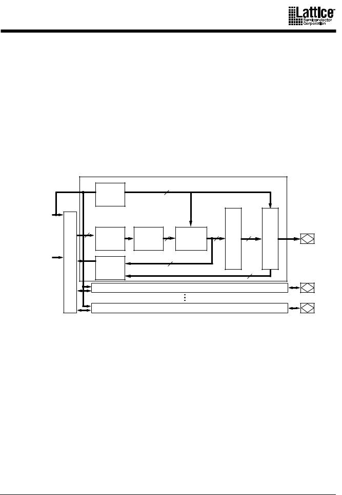
The fundamental architecture of MACH 4 devices (Figure 1) consists of multiple, optimized PAL® blocks interconnected by a central switch matrix. The central switch matrix allows communication between PAL blocks and routes inputs to the PAL blocks. Together, the PAL blocks and central switch matrix allow the logic designer to create large designs in a single device instead of having to use multiple devices.
The key to being able to make effective use of these devices lies in the interconnect schemes. In MACH 4 architecture, the macrocells are flexibly coupled to the product terms through the logic allocator, and the I/O pins are flexibly coupled to the macrocells due to the output switch matrix. In addition, more input routing options are provided by the input switch matrix. These resources provide the flexibility needed to fit designs efficiently.
|
|
|
|
|
|
|
|
PAL Block |
|
|
|
|
|
Clock |
|
4 |
|
Note 2 |
|
|
|
|
|
|
|
|
|
|
|
|
||
|
|
|
|
|
|
|
|
|
|
|
|
|
|
Generator |
|
|
|
|
|
|
|
Clock/Input |
MatrixSwitchCentral |
33/ |
|
|
|
|
MatrixSwitchOutput |
|
CellsI/O |
|
Pins |
|
|
|
|
|
|
||||
Note 3 |
|
34/ |
|
|
|
|
|
|
|
I/O |
|
|
36 |
Logic |
Logic |
16 |
Output/ |
16 |
8 |
|
Pins |
|
|
|
|
|
||||||
|
|
|
Allocator |
|
Buried |
|
|
|
|
|
|
|
|
Array |
|
|
|
|
|
||
|
|
|
with XOR |
|
Macrocells |
|
Note 1 |
|
|
|
|
|
|
|
|
|
|
|
|||
Dedicated |
|
|
|
|
16 |
|
|
|
|
|
Input Pins |
|
|
Input |
|
|
|
|
|
||
|
|
|
|
|
|
|
|
|
||
|
|
|
Switch |
|
|
|
|
16 |
|
I/O |
|
|
|
Matrix |
|
|
|
|
|
|
|
|
|
|
|
|
|
|
|
|
Pins |
|
|
|
|
|
|
|
|
|
|
|
|
|
|
|
|
|
|
PAL Block |
|
|
|
|
|
|
|
|
|
|
PAL Block |
|
|
|
|
|
|
|
|
|
|
|
|
|
|
I/O |
|
|
|
|
|
|
|
|
|
|
Pins |
|
|
|
|
|
|
|
|
|
|
17466G-001 |
Figure 1. MACH 4 Block Diagram and PAL Block Structure
Notes:
1.16 for MACH 4 devices with 1:1 macrocell-I/O cell ratio (see next page).
2.Block clocks do not go to I/O cells in M4(LV)-32/32.
3.M4(LV)-192/96 and M4(LV)-256/128 have dedicated clock pins which cannot be used as inputs and do not connect to the central switch matrix.
MACH 4 Family |
5 |

Table 4. Architectural Summary of MACH 4 devices
|
MACH 4 Devices |
|
|
|
|
|
|
|
M4-64/32, M4LV-64/32 |
|
|
|
M4-96/48, M4LV-96/48 |
|
|
|
M4-128/64, M4LV-128/64 |
|
M4-32/32 |
|
M4-128N/64, M4LV-128N/64 |
|
M4LV-32/32 |
|
M4-192/96, M4LV-192/96 |
|
|
|
M4-256/128, M4LV-256/128 |
|
|
|
|
|
|
Macrocell-I/O Cell |
2:1 |
|
1:1 |
Ratio |
|
||
|
|
|
|
|
|
|
|
Input Switch Matrix |
Yes |
|
Yes |
|
|
|
|
Input Registers |
Yes |
|
No |
|
|
|
|
Central Switch Matrix |
Yes |
|
Yes |
|
|
|
|
Output Switch Matrix |
Yes |
|
Yes |
|
|
|
|
The Macrocell-I/O cell ratio is defined as the number of macrocells versus the number of I/O cells internally in a PAL block (Table 4).
The central switch matrix takes all dedicated inputs and signals from the input switch matrices and routes them as needed to the PAL blocks. Feedback signals that return to the same PAL block still must go through the central switch matrix. This mechanism ensures that PAL blocks in MACH 4 devices communicate with each other with consistent, predictable delays.
The central switch matrix makes a MACH 4 device more advanced than simply several PAL devices on a single chip. It allows the designer to think of the device not as a collection of blocks, but as a single programmable device; the software partitions the design into PAL blocks through the central switch matrix so that the designer does not have to be concerned with the internal architecture of the device.
Each PAL block consists of:
Product-term array
Logic allocator
Macrocells
Output switch matrix
I/O cells
Input switch matrix
Clock generator
6 |
MACH 4 Family |

Product-Term Array
The product-term array consists of a number of product terms that form the basis of the logic being implemented. The inputs to the AND gates come from the central switch matrix (Table 5), and are provided in both true and complement forms for efficient logic implementation.
|
Table 5. PAL Block Inputs |
|
Device |
|
Number of Inputs to PAL Block |
|
|
|
M4-32/32 and M4LV-32/32 |
|
33 |
M4-64/32 and M4LV-64/32 |
|
33 |
M4-96/48 and M4LV-96/48 |
|
33 |
M4-128/64 and M4LV-128/64 |
|
33 |
M4-128N/64 and M4LV-128N/64 |
|
33 |
|
|
|
M4-192/96 and M4LV-192/96 |
|
34 |
M4-256/128 and M4LV-256/128 |
|
34 |
|
|
|
Logic Allocator
Within the logic allocator, product terms are allocated to macrocells in “product term clusters.” The availability and distribution of product term clusters are automatically considered by the software as it fits functions within a PAL block. The size of a product term cluster has been optimized to provide high utilization of product terms, making complex functions using many product terms possible. Yet when few product terms are used, there will be a minimal number of unused—or wasted—product terms left over. The product term clusters available to each macrocell within a PAL block are shown in Tables 6 and 7.
Each product term cluster is associated with a macrocell. The size of a cluster depends on the configuration of the associated macrocell. When the macrocell is used in synchronous mode (Figure 2a), the basic cluster has 4 product terms. When the associated macrocell is used in asynchronous mode (Figure 2b), the cluster has 2 product terms. Note that if the product term cluster is routed to a different macrocell, the allocator configuration is not determined by the mode of the macrocell actually being driven. The configuration is always set by the mode of the macrocell that the cluster will drive if not routed away, regardless of the actual routing.
In addition, there is an extra product term that can either join the basic cluster to give an extended cluster, or drive the second input of an exclusive-OR gate in the signal path. If included with the basic cluster, this provides for up to 20 product terms on a synchronous function that uses four extended 5-product-term clusters. A similar asynchronous function can have up to 18 product terms.
When the extra product term is used to extend the cluster, the value of the second XOR input can be programmed as a 0 or a 1, giving polarity control. The possible configurations of the logic allocator are shown in Figures 3 and 4.
MACH 4 Family |
7 |
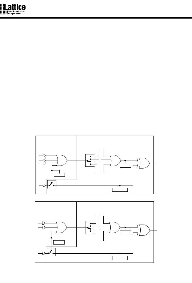
Table 6. Logic Allocator for All MACH 4 Devices (except M4(LV)-32/32)
Output Macrocell |
Available Clusters |
Output Macrocell |
Available Clusters |
|
|
|
|
M0 |
C0, C1, C2 |
M8 |
C7, C8, C9, C10 |
M1 |
C0, C1, C2, C3 |
M9 |
C8, C9, C10, C11 |
M2 |
C1, C2, C3, C4 |
M10 |
C9, C10, C11, C12 |
M3 |
C2, C3, C4, C5 |
M11 |
C10, C11, C12, C13 |
M4 |
C3, C4, C5, C6 |
M12 |
C11, C12, C13, C14 |
M5 |
C4, C5, C6, C7 |
M13 |
C12, C13, C14, C15 |
M6 |
C5, C6, C7, C8 |
M14 |
C13, C14, C15 |
M7 |
C6, C7, C8, C9 |
M15 |
C14, C15 |
Table 7. Logic Allocator for M4(LV)-32/32
Output Macrocell |
Available Clusters |
Output Macrocell |
Available Clusters |
|
|
|
|
M0 |
C0, C1, C2 |
M8 |
C8, C9, C10 |
M1 |
C0, C1, C2, C3 |
M9 |
C8, C9, C10, C11 |
M2 |
C1, C2, C3, C4 |
M10 |
C9, C10, C11, C12 |
M3 |
C2, C3, C4, C5 |
M11 |
C10, C11, C12, C13 |
M4 |
C3, C4, C5, C6 |
M12 |
C11, C12, C13, C14 |
M5 |
C4, C5, C6, C7 |
M13 |
C12, C13, C14, C15 |
M6 |
C5, C6, C7 |
M14 |
C13, C14, C15 |
M7 |
C6, C7 |
M15 |
C14, C15 |
|
|
1 2 |
n-1 |
Logic Allocator |
|
|
|
|
|
To n- |
To n- |
From |
|
|
|
Basic Product |
|
|
|
|
|||
|
|
|
|
|
|
|
|
Term Cluster |
|
|
|
|
|
|
|
|
n |
|
|
|
n |
Macrocell |
|
|
|
|
|
|
0 Default |
n |
|
|
|
|
|
|
|
To |
|
Extra |
0 Default |
n+1 |
n+1 |
n+2 |
|
|
|
Product |
|
|
|
|
|||
|
To |
From |
From |
|
|
|
|
Term |
|
|
|
|
|||
|
|
|
|
|
|||
|
|
|
|
|
Prog. Polarity |
|
|
a. Synchronous Mode
|
|
1 2 |
n-1 |
Logic Allocator |
|
|
|
|
|
To n- |
To n- |
From |
|
|
|
Basic Product |
|
|
|
|
|||
|
|
|
|
|
|
|
|
Term Cluster |
|
|
|
|
|
|
|
|
n |
|
|
|
n |
Macrocell |
n |
|
|
|
|
|
0 Default |
||
|
|
|
|
|
|
||
|
|
|
|
|
|
To |
|
Extra |
0 Default |
n+1 |
n+1 |
n+2 |
|
|
|
Product |
|
|
|
|
|||
|
To |
From |
From |
|
|
|
|
Term |
|
|
|
|
|||
|
|
|
|
|
|||
|
|
|
|
|
Prog. Polarity |
|
|
b. Asynchronous Mode
Figure 2. Logic Allocator: Configuration of Cluster “n” Set by Mode of Macrocell “n”
17466G-005
17466G-006
8 |
MACH 4 Family |
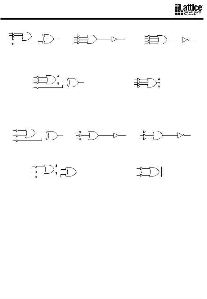
a. Basic cluster with XOR |
b. Extended cluster, active high |
c. Extended cluster, active low |
|

 0
0
d. Basic cluster routed away; |
e. Extended cluster routed away |
single-product-term, active high |
|
17466G-007
Figure 3. Logic Allocator Configurations: Synchronous Mode
a. Basic cluster with XOR |
b. Extended cluster, active high |
c. Extended cluster, active low |

 0
0
d. Basic cluster routed away; |
e. Extended cluster routed away |
single-product-term, active high |
|
17466G-008
Figure 4. Logic Allocator Configurations: Asynchronous Mode
Note that the configuration of the logic allocator has absolutely no impact on the speed of the signal. All configurations have the same delay. This means that designers do not have to decide between optimizing resources or speed; both can be optimized.
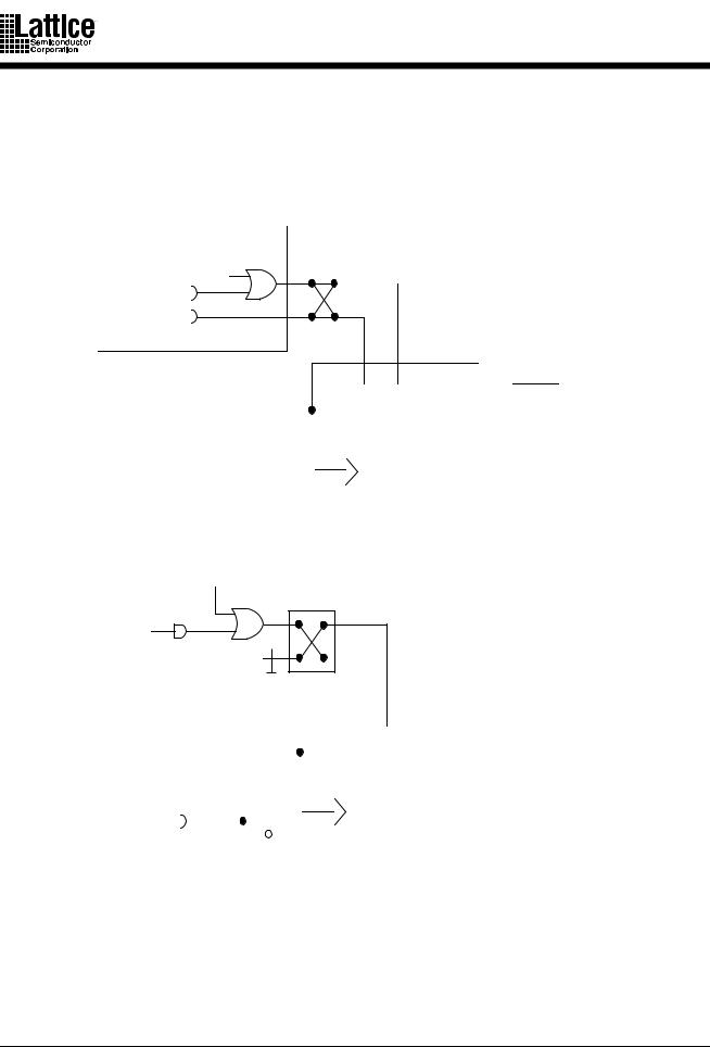
If not used in the cluster, the extra product term can act in conjunction with the basic cluster to provide XOR logic for such functions as data comparison, or it can work with the D-,T-type flipflop to provide for J-K, and S-R register operation. In addition, if the basic cluster is routed to another macrocell, the extra product term is still available for logic. In this case, the first XOR input will be a logic 0. This circuit has the flexibility to route product terms elsewhere without giving up the use of the macrocell.
Product term clusters do not “wrap” around a PAL block. This means that the macrocells at the ends of the block have fewer product terms available.
MACH 4 Family |
9 |
Macrocell
The macrocell consists of a storage element, routing resources, a clock multiplexer, and initialization control. The macrocell has two fundamental modes: synchronous and asynchronous (Figure 5). The mode chosen only affects clocking and initialization in the macrocell.
Power-Up
Reset
PAL-Block |
|
|
|
|
|
|
|
|
|
|
|
|
|
|
|
|
|
|
|
|
|
|
|
|
|
|
|
|
|
|
|
|
|
|
|
|
|
|
|
|
|
|
|
|
|
|
|
|
|
|
|
|
|
|
|
|
|
|
|
|
|
|
|
|
|
|
|
|
|
|
|
|
|
|
Initialization |
|
|
|
|
|
|
|
|
|
|
|
|
|
|
|
|
|
|
|
|
|
|
|
|
|
|
|
||
Product Terms |
|
|
|
|
|
|
SWAP |
|
|
|
|
|
||
|
|
|
|
|
|
|
|
|
|
|
||||
|
|
|
|
|
|
|
|
|
|
|||||
Common PAL-block resource |
|
|
|
|
|
|
||||||||
|
|
|
|
|
|
|
|
|
||||||
Individual macrocell resources |
|
|
|
|
|
|
|
|
|
|||||
|
|
|
|
|
|
|
|
|
|
|
|
|
|
|
From Logic Allocator |
|
|
|
|
|
|
|
|
|
AP |
AR |
|
|
|
|
|
|
|
|
|
|
|
|
D/T/L |
|
Q |
|
|
|
|
|
|
Block CLK0 |
|
|
|
|
|
|
|||||
From |
|
|
|
|
|
|
|
|
|
|
|
|||
|
|
|
|
|
|
|
|
|
|
|
||||
|
|
|
|
|
|
|
|
|
||||||
|
|
Block CLK1 |
|
|
|
|
|
|
|
|
|
|||
PAL-Clock |
|
|
|
|
|
|
|
|
|
|
|
|||
|
|
Block CLK2 |
|
|
|
|
|
|
|
|
|
|||
Generator |
|
|
|
|
|
|
|
|
|
|
|
|||
|
|
Block CLK3 |
|
|
|
|
|
|
|
|
|
|||
|
|
|
|
|
|
|
|
|
|
|
|
|
||
|
|
|
|
|
|
|
|
|
|
|
|
|
|
|
|
|
|
|
|
|
|
|
|
|
|
|
|||
|
|
|
|
|
|
a. Synchronous mode |
|
|
||||||
Power-Up
Reset
Individual
Initialization
Product Term
|
|
|
|
|
|
|
|
|
|
|
|
|
|
|
|
|
|
|
|
|
|
|
|
|
|
|
|
|
|
|
|
|
|
|
|
|
|
|
|
|
|
|
|
|
|
|
|
|
|
|
|
|
|
|
|
|
|
|
|
|
|
|
|
|
|
|
|
|
|
|
|
|
|
|
|
|
|
|
|
|
|
|
|
|
|
|
|
|
|
|
|
|
|
|
From Logic |
|
|
|
|
|
|
|
|
|
|
|
AP |
AR |
|
|
|
||
|
|
|
|
|
|
|
|
|
|
|
D/T/L |
Q |
|
|
|
|||
Allocator |
|
|
|
|
|
|
|
|
|
|
|
|
|
|
||||
|
|
|
|
|
|
|
|
|
|
|
|
|
|
|||||
From PAL-Block |
|
|
|
Block CLK0 |
|
|
|
|
|
|
|
|
|
|
||||
|
|
|
|
|
|
|
|
|
|
|||||||||
Clock Generator |
|
|
|
Block CLK1 |
|
|
|
|
|
|
|
|
|
|
||||
Individual Clock |
|
|
|
|
|
|
|
|
|
|
|
|
|
|
|
|
|
|
|
|
|
|
|
|
|
|
|
|
|
|
|
|
|
|
|
||
Product Term |
|
|
|
|
|
|
|
|
|
|
|
|
|
|
|
|
|
|
|
|
|
|
|
|
|
|
|
|
|
|
|
|
|
|
|
||
|
|
|
|
|
|
|
|
|
|
|
|
|
|
|
|
|||
|
|
|
|
|
|
|
|
|
|
b. Asynchronous mode |
|
|
||||||
Figure 5. Macrocell
To Output and Input
Switch Matrices
17466G-009
To Output and Input
Switch Matrices
17466G-010
In either mode, a combinatorial path can be used. For combinatorial logic, the synchronous mode will generally be used, since it provides more product terms in the allocator.
10 |
MACH 4 Family |

The flip-flop can be configured as a D-type or T-type latch. J-K or S-R registers can be synthesized. The primary flip-flop configurations are shown in Figure 6, although others are possible. Flip-flop functionality is defined in Table 8. Note that a J-K latch is inadvisable as it will cause oscillation if both J and K inputs are HIGH.
AP AR
D Q
AP AR D Q
a. D-type with XOR |
b. D-type with programmable D polarity |
||
|
AP AR |
AP AR |
|
L |
Q |
L |
Q |
|
|
|
|
G |
|
|
|
|
|
G |
|
|
|
|
|
|
|
|
|
|
|||
|
|
|
|
|
|
|
|
|
|||
|
|
|
|
|
|
|
|
|
|||
|
|
|
|
|
|
|
|
|
|
|
|
|
|
|
|
|
|
|
|
|
|
|
|
c. Latch with XOR |
d. Latch with programmable D polarity |
||||||||||
AP AR
T Q
f. Combinatorial with XOR
e. T-type with programmable T polarity
g. Combinatorial with programmable polarity
17466G-011
Figure 6. Primary Macrocell Configurations
MACH 4 Family |
11 |
Table 8. Register/Latch Operation
Configuration |
Input(s) |
CLK/LE 1 |
Q+ |
||
|
D=X |
0,1, ↓ (↑) |
|
Q |
|
D-type Register |
D=0 |
↑ (↓) |
0 |
|
|
|
D=1 |
↑ (↓) |
1 |
|
|
|
|
|
|
|
|
|
T=X |
0, 1, ↓ (↑) |
|
Q |
|
T-type Register |
T=0 |
↑ (↓) |
|
Q |
|
|
T=1 |
↑ (↓) |
|
|
|
|
|
Q |
|
||
|
|
|
|
|
|
|
D=X |
1(0) |
|
Q |
|
D-type Latch |
D=0 |
0(1) |
0 |
|
|
|
D=1 |
0(1) |
1 |
|
|
|
|
|
|
|
|
Note:
1. Polarity of CLK/LE can be programmed
Although the macrocell shows only one input to the register, the XOR gate in the logic allocator allows the D-, T-type register to emulate J-K, and S-R behavior. In this case, the available product terms are divided between J and K (or S and R). When configured as J-K, S-R, or T-type, the extra product term must be used on the XOR gate input for flip-flop emulation. In any register type, the polarity of the inputs can be programmed.
The clock input to the flip-flop can select any of the four PAL block clocks in synchronous mode, with the additional choice of either polarity of an individual product term clock in the asynchronous mode.
The initialization circuit depends on the mode. In synchronous mode (Figure 7), asynchronous reset and preset are provided, each driven by a product term common to the entire PAL block.
|
Power-Up |
Power-Up |
|
Reset |
|
|
Preset |
|
|
|
|
PAL-Block |
|
PAL-Block |
Initialization |
|
|
|
Initialization |
|
Product Terms |
|
|
|
Product Terms |
|
|
|
AP AR D/T/L Q
AP |
AR |
D/L |
Q |
a. Power-up reset |
b. Power-up preset |
17466G-012 |
17466G-013 |
Figure 7. Synchronous Mode Initialization Configurations
12 |
MACH 4 Family |
A reset/preset swapping feature in each macrocell allows for reset and preset to be exchanged, providing flexibility. In asynchronous mode (Figure 8), a single individual product term is provided for initialization. It can be selected to control reset or preset.
|
Power-Up |
|
|
|
|
Power-Up |
|
|||||||||||||||||
|
|
Reset |
|
|
|
|
|
Preset |
|
|||||||||||||||
Individual |
|
|
|
|
|
|
|
|
|
Individual |
|
|
|
|
|
|
||||||||
|
|
|
|
|
|
|
|
|
|
|
|
|
||||||||||||
|
|
|
|
|
|
|
|
|
|
|
||||||||||||||
|
|
|
|
|
|
|
|
Preset |
|
|
|
|
|
|
|
|
|
|||||||
Reset |
|
|
|
|
|
|
|
|
|
|
|
|
|
|
|
|
|
|
|
|
|
|||
|
|
|
|
|
|
|
|
|
|
|
|
|
|
|
|
|
|
|
||||||
Product Term |
|
|
Product Term |
|
|
|
|
|
||||||||||||||||
|
|
|
|
|
|
|
|
|
|
|
|
|||||||||||||
|
|
|
|
|
|
|
|
|
|
|
|
|
|
|
|
|
|
|
|
|
|
|
|
|
|
|
|
|
|
|
|
|
|
|
|
|
|
|
|
|
|
|
|
|
|
|
|
|
|
|
|
|
|
|
|
|
|
|
|
|
|
|
|
|
|
|
|
|
|
|
|
|
|
|
|
|
|
|
|
|
|
|
|
|
|
|
|
|
|
|
|
|
|
|
|
|
|
|
|
|
|
|
|
|
|
|
|
|
|
AP |
AR |
|
|
|
|
|
|
|
AP |
AR |
||||
|
|
|
|
|
|
|
|
|
|
D/L/T |
Q |
|
|
|
|
|
|
|
D/L/T |
Q |
||||
|
|
|
|
|
|
|
|
|
|
|
|
|
|
|
|
|
|
|
|
|
|
|
|
|
a. Reset |
b. Preset |
17466G-014 |
17466G-015 |
Figure 8. Asynchronous Mode Initialization Configurations
Note that the reset/preset swapping selection feature effects power-up reset as well. The initialization functionality of the flip-flops is illustrated in Table 9. The macrocell sends its data to the output switch matrix and the input switch matrix. The output switch matrix can route this data to an output if so desired. The input switch matrix can send the signal back to the central switch matrix as feedback.
Table 9. Asynchronous Reset/Preset Operation
AR |
AP |
CLK/LE1 |
Q+ |
0 |
0 |
X |
See Table 8 |
|
|
|
|
0 |
1 |
X |
1 |
|
|
|
|
1 |
0 |
X |
0 |
|
|
|
|
1 |
1 |
X |
0 |
|
|
|
|
Note:
1. Transparent latch is unaffected by AR, AP
MACH 4 Family |
13 |
Output Switch Matrix
The output switch matrix allows macrocells to be connected to any of several I/O cells within a PAL block. This provides high flexibility in determining pinout and allows design changes to occur without effecting pinout.
In MACH 4 devices with 2:1 Macrocell-I/O cell ratio, each PAL block has twice as many macrocells as I/O cells. The MACH 4 output switch matrix allows for half of the macrocells to drive I/O cells within a PAL block, in combinations according to Figure 9. Each I/O cell can choose from eight macrocells; each macrocell has a choice of four I/O cells. The MACH 4 devices with 1:1 Macrocell-I/O cell ratio allow each macrocell to drive one of eight I/O cells (Figure 9).
macrocells |
MUX |
I/O cell |
Each I/O cell can choose one of 8 macrocells in all MACH 4 devices.
M0 |
|
M1 |
|
M2 |
|
M3 |
|
M4 |
I/O0 |
M5 |
I/O1 |
M6 |
I/O2 |
M7 |
I/O3 |
M8 |
I/O4 |
M9 |
I/O5 |
M10 |
I/O6 |
M11 |
I/O7 |
M12 |
|
M13
M14
M15
Each macrocell can drive one of 4 I/O cells in MACH 4 devices with
2:1 macrocell-I/O cell ratio.
M0 |
I/O0 |
M1 |
I/O1 |
M2 |
I/O2 |
M3 |
I/O3 |
M4 |
I/O4 |
M5 |
I/O5 |
M6 |
I/O6 |
M7 |
I/O7 |
|
|
|
|
M8 |
I/O8 |
M9 |
I/O9 |
M10 |
I/O10 |
M11 |
I/O11 |
M12 |
I/O12 |
M13 |
I/O13 |
M14 |
I/O14 |
M15 |
I/O15 |
|
|
Each macrocell can drive one of 8 I/O cells in M4(LV)-32/32 devices.
Figure 9. MACH 4 Output Switch Matrix
14 |
MACH 4 Family |
 Loading...