


IS93C66-3PI
ISSI IS93C66-3PI, IS93C66-3P, IS93C66-3GRI, IS93C66-3GI, IS93C66-3G Datasheet
...
Integrated Silicon Solution, Inc. — 1-800-379-4774
1
Rev. G
04/26/01
ISSI reserves the right to make changes to its products at any time without notice in order to improve design and supply the best possible product. We assume no responsibility for any
errors which may appear in this publication. © Copyright 2001, Integrated Silicon Solution, Inc.
IS93C66-3
ISSI
®
4,096-BIT SERIAL ELECTRICALLY
ERASABLE PROM
OVERVIEW
The IS93C66-3 is a low cost 4,096-bit, non-volatile, serial
E
2
PROM. It is fabricated using ISSI's advanced CMOS
E
2
PROM technology. The IS93C66-3 provides efficient
non-volatile read/write memory arranged as 256 registers
of 16 bits each. Seven 11-bit instructions control the
operation of the device, which includes read, write, and
mode enable functions. The data out pin (DOUT) indicates
the status of the device during in the self-timed non-volatile
programming cycle.
The self-timed write cycle includes an automatic erase-
before-write capability. To protect against inadvertent
writes, the WRITE instruction is accepted only while the
chip is in the write enabled state. Data is written in 16 bits
per write instruction into the selected register. If Chip
Select
(CS)
is brought
HIGH
after initiation of the write cycle,
the Data Output (DOUT) pin will indicate the
READY/BUSY
status of the chip.
APPLICATIONS
The IS93C66-3 is ideal for high-volume applications
requiring low power and low density storage. This device
uses a low cost, space saving 8-pin package. Candidate
applications include robotics, alarm devices, electronic
locks, meters and instrumentation settings.
MARCH 2001
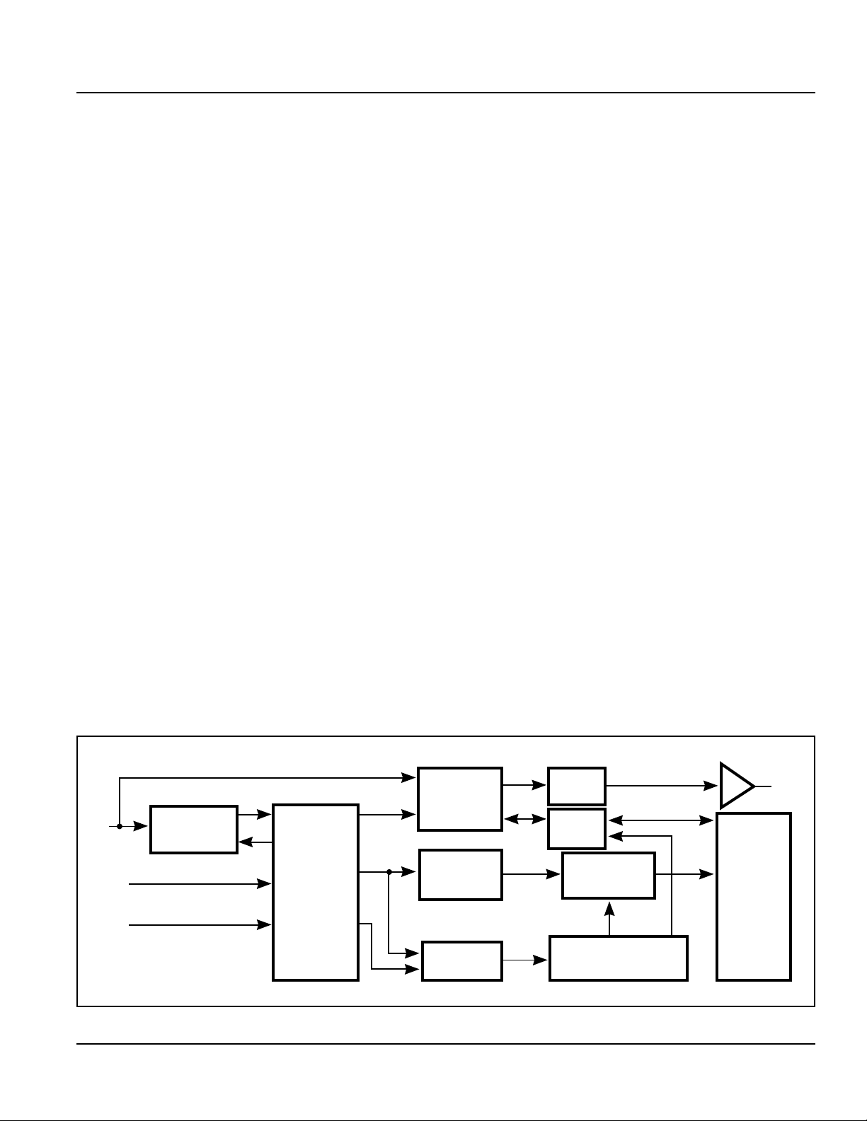
FUNCTIONAL BLOCK DIAGRAM
FEATURES
• State-of-the-art architecture
— Non-volatile data storage
— Low voltage operation:
3.0V (Vcc = 2.7V to 6.0V)
— Full TTL compatible inputs and outputs
— Auto increment for efficient data dump
• Low voltage read operation
— Down to 2.7V
• Hardware and software write protection
— Defaults to write-disabled state at power-up
— Software instructions for write-enable/disable
• Advanced low voltage CMOS E
2
PROM
technology
• Versatile, easy-to-use interface
— Self-timed programming cycle
— Automatic erase-before-write
— Programming status indicator
— Word and chip erasable
— Stop SK anytime for power savings
• Durable and reliable
— 10-year data retention after 100K write cycles
— 100,000 write cycles
— Unlimited read cycles
CS
SK
D
IN
D
OUT
DUMMY
BIT
R/W
AMPS
DATA
REGISTER
(16 BITS)
ADDRESS
REGISTER
1 OF 256
DECODER
WRITE
ENABLE
HIGH VOLTAGE
GENERATOR
INSTRUCTION
DECODE,
CONTROL,
AND
CLOCK
GENERATION
INSTRUCTION
REGISTER
(11 BITS)
EEPROM
ARRAY
(256 X 16)
2
Integrated Silicon Solution, Inc. — 1-800-379-4774
Rev. G
04/26/01
IS93C66-3
ISSI
®
PIN CONFIGURATION
8-Pin DIP
1
2
3
4
8
7
6
5
CS
SK
D
IN
D
OUT
VCC
NC
NC
GND
PIN CONFIGURATION
8-Pin
JEDEC
Small Outline
“G”
PIN CONFIGURATION
8-Pin
JEDEC
Small Outline
“GR”
1
2
3
4
8
7
6
5
NC
VCC
CS
SK
NC
GND
D
OUT
D
IN
1
2
3
4
8
7
6
5
CS
SK
D
IN
D
OUT
VCC
NC
NC
GND
PIN DESCRIPTIONS
CS Chip Select
SK Serial Data Clock
DIN Serial Data Input
DOUT Serial Data Output
NC Not Connected
Vcc Power
GND Ground
Low Voltage Read
The IS93C66-3 has been designed to ensure that data
read operations are reliable in low voltage environments.
The IS93C66-3 is guaranteed to provide accurate data
during read operations with Vcc as low as 2.7V.
Auto Increment Read Operations
In the interest of memory transfer operation applications,
the IS93C66-3 has been designed to output a continuous
stream of memory content in response to a single read
operation instruction. To utilize this function, the system
asserts a read instruction specifying a start location
address. Once the 16 bits of the addressed word have
been clocked out, the data in consecutively higher address
locations (the address
“000000”
is assumed as the ad-
dress of
“111111"
) is output. The address will wrap around
continuously with
CS HIGH
until the chip select
(CS)
control pin is brought
LOW
. This allows for single instruction
data dumps to be executed with a minimum of firmware
overhead.
Write Enable (WEN)
The write enable (WEN) instruction must be executed
before any device programming (WRITE, WRALL, ERASE,
and ERAL) can be done. When Vcc is applied, this device
powers up in the write disabled state. The device then
ENDURANCE AND DATA RETENTION
The IS93C66-3 is designed for applications requiring up
to 100,000 programming cycles (WRITE, WRALL, ERASE
and ERAL). It provides 10 years of secure data retention,
without power after the execution of 100,000 programming
cycles.
DEVICE OPERATION
The IS93C66-3 is controlled by seven 11-bit instructions.
Instructions are clocked in (serially) on the DIN pin. Each
instruction begins with a logical “1” (the start bit). This is
followed by the opcode (2 bits), the address field (8 bits),
and data, if appropriate. The clock signal (SK) may be
halted at any time and the IS93C66-3 will remain in its last
state. This allows full static flexibility and maximum
power conservation.
Read (READ)
The READ instruction is the only instruction that outputs
serial data on the DOUT pin. After the read instruction and
address have been decoded, data is transferred from the
selected memory register into a 16-bit serial shift register.
(Please note that one logical “0” bit precedes the actual
16-bit output data string.) The output on DOUT changes
during the low-to-high transitions of SK (see Figure 3).

Integrated Silicon Solution, Inc. — 1-800-379-4774
3
Rev. G
04/26/01
IS93C66-3
ISSI
®
As with the WRITE instruction, if CS is brought HIGH after
a minimum wait of 250 ns (tCS), the DOUT pin indicates the
READY/BUSY status of the chip (see Figure 6).
W
rite Disable (WDS)
The write disable (WDS) instruction disables all
programming capabilities. This protects the entire part
against accidental modification of data until a WEN
instruction is executed. (When Vcc is applied, this part
powers up in the write disabled state.) To protect data, a
WDS instruction should be executed upon completion of
each programming operation. (NOTE: Neither the WEN
nor the WDS instruction has any effect on the READ
instruction.) (See Figure 7.)
Erase Register (ERASE)
After the erase instruction is entered, CS must be brought
LOW. The falling edge of CS initiates the self-timed
internal programming cycle. Bringing CS HIGH after a
minimum of tCS, will cause DOUT to indicate the
READ/BUSY
status of the chip: a logical “0” indicates programming is
still in progress; a logical “1” indicates the erase cycle is
complete and the part is ready for another instruction (see
Figure 8).
Erase All (ERAL)
Full chip erase is provided for ease of programming.
Erasing the entire chip involves setting all bits in the entire
memory array to a logical “1” (see Figure 9).
remains in a write disabled state until a WEN instruction
is executed. Thereafter, the device remains enabled until
a WDS instruction is executed or until Vcc is removed.
(NOTE: Neither the WEN nor the WDS instruction has any
effect on the READ instruction.) (See Figure 4.)
Write (WRITE)
The WRITE instruction includes 16 bits of data to be
written into the specified register. After the last data bit
has been applied to DIN, and before the next rising edge of
SK, CS must be brought LOW. The falling edge of CS
initiates the self-timed programming cycle.
After a minimum wait of 250 ns (5V operation) from the
falling edge of CS (tCS), if CS is brought HIGH, DOUT will
indicate the READY/BUSY status of the chip: logical “0”
means programming is still in progress; logical “1” means
the selected register has been written, and the part is
ready for another instruction (see Figure 5). (NOTE: The
combination of CS HIGH, DIN HIGH and the rising edge of
the SK clock, resets the READY/BUSY flag. Therefore, it
is important if you want to access the READY/BUSY flag
not to reset it through this combination of control signals.)
Before a WRITE instruction can be executed, the device
must be write enabled (see WEN).
Write All (WRALL)
The write all (WRALL) instruction programs all registers
with the data pattern specified in the instruction. While the
WRALL instruction is being loaded, the address field
becomes a sequence of “Don’t Care” bits (see Figure 6).
INSTRUCTION SET
Instruction Start Bit OP Code Address Input Data
READ 1 10 (A7-A0)
WEN 1 00 11XXXXXX
(Write Enable)
WRITE 1 01 (A7-A0) D15-D0
(1)
WRALL 1 00 01XXXXXX D15-D0
(1)
(Write All Registers)
WDS 1 00 00XXXXXX
(Write Disable)
ERASE 1 11 (A7-A0)
ERAL 1 00 10XXXXXX
(Erase All Registers)
Note: 1. If input data is not 16 bits exactly, the last 16 bits will be taken as input data (a word).
 Loading...