


ISSI IS62V6416BLL-12TI, IS62V6416BLL-12T, IS62V6416BLL-12KI, IS62V6416BLL-12K, IS62V6416BLL-12BI Datasheet
...IS62V6416BLL |
ISSI® |
64K x 16 LOW VOLTAGE,
ULTRA LOW POWER CMOS STATIC RAM
MARCH 2000
FEATURES
•Access time: 100 and 120 ns
•CMOS low power operation
•TTL compatible interface levels
•Single 2.7V-3.3V power supply
•Fully static operation: no clock or refresh required
•Three state outputs
•Data control for upper and lower bytes
•Industrial temperature available
•Available in Jedec Std 44-pin SOJ package, 44-pin TSOP (Type II), and 48-pin mini BGA
DESCRIPTION
The ISSI IS62V6416BLL is an ultra-low power, 1,048,576-bit static RAM organized as 65,536 words by 16 bits. It is fabricated using ISSI's high-performance CMOS technology. This highly reliable process coupled with innovative circuit design techniques yields access times as fast as 100 ns with low power consumption.
When CS is HIGH (deselected) or when CS is LOW and both LB and UB are HIGH, the device assumes a standby mode at which the power dissipation can be reduced down with CMOS input levels.
Easy memory expansion is provided by using Chip Select and Output Enable inputs, CS and OE. The active LOW Write Enable (WE) controls both writing and reading of the memory. A data byte allows Upper Byte (UB) and Lower Byte (LB) access.
FUNCTIONAL BLOCK DIAGRAM
|
|
|
|
|
|
|
|
|
|
|
|
|
|
|
|
|
|
|
|
|
|
|
|
A0-A15 |
|
|
|
|
|
|
|
|
|
|
|
|
|
|
DECODER |
|
|
64K x 16 |
|
||||
|
|
|
|
|
|
|
|
|
|
|
|
|
|
|
|
MEMORY ARRAY |
|
||||||
|
|
|
|
|
|
|
|
|
|
|
|
|
|
|
|
|
|
|
|
|
|||
VCC |
|
|
|
|
|
|
|
|
|
|
|
|
|
|
|
|
|
|
|
|
|
|
|
|
|
|
|
|
|
|
|
|
|
|
|
|
|
|
|
|
|
|
|
|
|
|
|
|
|
|
|
|
|
|
|
|
|
|
|
|
|
|
|
|
|
|
|
|
|
|
|
GND |
|
|
|
|
|
|
|
|
|
|
|
|
|
|
|
|
|
|
|
|
|
|
|
|
|
|
|
|
|
|
|
|
|
|
|
|
|
|
|
|
|
|
|
|
|
|
|
I/O0-I/O7 |
|
|
|
|
|
|
|
|
|
|
|
|
|
|
|
|
|
|
|
|
|
|
|
|
|
|
|
|
|
|
|
|
|
|
|
|
|
I/O |
|
|
|
|
|
|
|
||
|
|
|
|
|
|
|
|
|
|
|
|
|
|
|
|
|
|
|
|
|
|||
Lower Byte |
|
|
|
|
|
|
|
|
|
|
|
|
|
|
|
|
COLUMN I/O |
|
|
||||
|
|
|
|
|
|
|
|
|
|
|
|
|
|
DATA |
|
|
|
|
|
||||
|
|
|
|
|
|
|
|
|
|
|
|
|
|
|
|
|
|
|
|||||
I/O8-I/O15 |
|
|
|
|
|
|
|
|
|
|
|
|
|
|
CIRCUIT |
|
|
|
|
|
|
||
|
|
|
|
|
|
|
|
|
|
|
|
|
|
|
|
|
|
|
|
|
|
|
|
Upper Byte |
|
|
|
|
|
|
|
|
|
|
|
|
|
|
|
|
|
|
|
|
|
|
|
|
|
|
|
|
|
|
|
|
|
|
|
|
|
|
|
|
|
|
|
|
|
|
|
|
|
|
|
|
|
|
|
|
|
|
|
|
|
|
|
|
|
|
|
|
|
|
|
|
|
|
|
|
|
|
|
|
|
|
|
|
|
|
|
|
|
|
|
|
|
|
|
|
|
|
|
|
|
|
|
|
|
|
|
|
|
|
|
|
|
|
|
|
|
||
|
CS |
|
|
|
|
|
|
|
|
|
|
|
|||||||||||
|
|
|
|
|
|
|
|
|
|
|
|
|
|
|
|
|
|
|
|
|
|||
|
|
|
|
|
|
|
|
|
|
|
|
|
|
|
|
|
|
|
|
||||
|
OE |
|
|
CONTROL |
|
|
|
|
|
|
|||||||||||||
|
|
|
|
|
|
|
|
|
|
|
|
|
|
|
|
||||||||
|
WE |
|
|
|
|
|
|
|
|
|
|
|
|||||||||||
|
|
|
|
|
|
CIRCUIT |
|
|
|
|
|
|
|||||||||||
|
|
|
|
|
|
|
|
|
|
||||||||||||||
|
|
|
|
|
|
|
|
|
|
|
|
|
|
|
|
|
|
|
|
|
|||
|
|
|
|
|
UB |
|
|
|
|
|
|
|
|
|
|
|
|
|
|
||||
|
|
|
|
|
|
|
|
|
|
|
|
|
|
||||||||||
|
|
|
|
|
|
|
|
|
|
|
|
|
|
|
|
|
|
||||||
|
|
|
|
|
|
LB |
|
|
|
|
|
|
|
|
|
|
|
|
|
|
|||
|
|
|
|
|
|
|
|
|
|
|
|
|
|
|
|
||||||||
|
|
|
|
|
|
|
|
|
|
|
|
|
|
|
|
|
|
|
|
|
|
|
|
|
|
|
|
|
|
|
|
|
|
|
|
|
|
|
|
|
|
|
|
|
|
|
|
ISSI reserves the right to make changes to its products at any time without notice in order to improve design and supply the best possible product. We assume no responsibility for any errors which may appear in this publication. © Copyright 2000, Integrated Silicon Solution, Inc.
Integrated Silicon Solution, Inc. — 1-800-379-4774 |
1 |
Rev. A
03/17/00

IS62V6416BLL |
ISSI® |
PIN CONFIGURATIONS
44-Pin SOJ
|
|
|
|
|
|
44 |
|
A5 |
|||||
|
|
A4 |
|
1 |
|
||||||||
|
|
A3 |
|
43 |
|
A6 |
|||||||
|
|
|
2 |
|
|||||||||
|
|
A2 |
|
42 |
|
A7 |
|||||||
|
|
|
3 |
|
|||||||||
|
|
A1 |
|
41 |
|
|
|
|
|
|
|
||
|
|
|
4 |
|
|
|
OE |
|
|||||
|
|
A0 |
|
40 |
|
|
|
|
|
|
|
||
|
|
|
5 |
|
|
UB |
|
||||||
|
|
|
|
|
|
|
|
|
|
|
|
|
|
|
|
CS |
|
|
6 |
39 |
|
LB |
|||||
I/O0 |
|
38 |
|
I/O15 |
|||||||||
|
7 |
|
|||||||||||
I/O1 |
|
8 |
37 |
|
I/O14 |
||||||||
|
|
||||||||||||
I/O2 |
|
36 |
|
I/O13 |
|||||||||
|
9 |
|
|||||||||||
I/O3 |
|
35 |
|
I/O12 |
|||||||||
|
10 |
|
|||||||||||
Vcc |
|
34 |
|
GND |
|||||||||
|
11 |
|
|||||||||||
GND |
|
33 |
|
Vcc |
|||||||||
|
12 |
|
|||||||||||
I/O4 |
|
32 |
|
I/O11 |
|||||||||
|
13 |
|
|||||||||||
I/O5 |
|
31 |
|
I/O10 |
|||||||||
|
14 |
|
|||||||||||
I/O6 |
|
15 |
30 |
|
I/O9 |
||||||||
|
|
||||||||||||
I/O7 |
|
16 |
29 |
|
I/O8 |
||||||||
|
|
||||||||||||
|
|
|
|
|
17 |
28 |
|
NC |
|||||
WE |
|
|
|||||||||||
A15 |
|
18 |
27 |
|
A8 |
||||||||
|
|
||||||||||||
A14 |
|
19 |
26 |
|
A9 |
||||||||
|
|
||||||||||||
A13 |
|
20 |
25 |
|
A10 |
||||||||
|
|
||||||||||||
A12 |
|
21 |
24 |
|
A11 |
||||||||
|
|
||||||||||||
|
NC |
|
22 |
23 |
|
NC |
|||||||
|
|
||||||||||||
|
|
|
|
|
|
|
|
|
|
|
|
|
|
48-Pin mini BGA (Top View)
1 |
2 |
3 |
4 |
5 |
6 |
A |
LB |
OE |
A0 |
A1 |
A2 |
N/C |
|
B |
I/O |
UB |
A3 |
A4 |
CS |
I/O |
|
8 |
0 |
||||||
|
|
|
|
|
|||
C |
I/O |
I/O |
A5 |
A6 |
I/O |
I/O |
|
9 |
10 |
1 |
2 |
||||
|
|
|
|||||
D |
GND |
I/O |
NC |
A7 |
I/O |
Vcc |
|
11 |
3 |
||||||
|
|
|
|
|
|||
E |
Vcc |
I/O |
NC |
NC |
I/O |
GND |
|
12 |
4 |
||||||
|
|
|
|
|
|||
F |
I/O |
I/O |
A14 |
A15 |
I/O |
I/O |
|
14 |
13 |
5 |
6 |
||||
|
|
|
|||||
G |
I/O |
NC |
A12 |
A13 |
WE |
I/O |
|
15 |
7 |
||||||
H |
NC |
A8 |
A9 |
A10 |
A11 |
NC |
44-Pin TSOP
|
|
|
|
|
44 |
|
A5 |
|||
|
A4 |
1 |
|
|||||||
|
A3 |
|
2 |
43 |
|
A6 |
||||
|
|
|||||||||
|
A2 |
|
3 |
42 |
|
A7 |
||||
|
|
|||||||||
|
A1 |
|
4 |
41 |
|
|
|
|||
|
|
|
|
OE |
|
|||||
|
A0 |
|
5 |
40 |
|
|
|
|||
|
|
|
|
UB |
|
|||||
|
CS |
|
6 |
39 |
|
|
||||
|
|
|
|
LB |
|
|||||
I/O0 |
|
7 |
38 |
|
I/O15 |
|||||
|
|
|||||||||
I/O1 |
|
8 |
37 |
|
I/O14 |
|||||
|
|
|||||||||
I/O2 |
|
9 |
36 |
|
I/O13 |
|||||
|
|
|||||||||
I/O3 |
|
10 |
35 |
|
I/O12 |
|||||
|
|
|||||||||
|
Vcc |
|
34 |
|
GND |
|||||
|
|
11 |
|
|||||||
GND |
|
33 |
|
Vcc |
||||||
|
12 |
|
||||||||
I/O4 |
|
13 |
32 |
|
I/O11 |
|||||
|
|
|||||||||
I/O5 |
|
14 |
31 |
|
I/O10 |
|||||
|
|
|||||||||
I/O6 |
|
15 |
30 |
|
I/O9 |
|||||
|
|
|||||||||
I/O7 |
|
16 |
29 |
|
I/O8 |
|||||
|
|
|||||||||
|
|
|
|
17 |
28 |
|
NC |
|||
|
WE |
|
|
|
||||||
A15 |
|
18 |
27 |
|
A8 |
|||||
|
|
|||||||||
A14 |
|
19 |
26 |
|
A9 |
|||||
|
|
|||||||||
A13 |
|
20 |
25 |
|
A10 |
|||||
|
|
|||||||||
A12 |
|
21 |
24 |
|
A11 |
|||||
|
|
|||||||||
|
NC |
|
22 |
23 |
|
NC |
||||
|
|
|
||||||||
|
|
|
|
|
|
|
|
|
|
|
PIN DESCRIPTIONS
A0-A15 |
Address Inputs |
I/O0-I/O15 |
Data Inputs/Outputs |
|
|
CS |
Chip Enable Input |
|
|
OE |
Output Enable Input |
|
|
WE |
Write Enable Input |
|
|
LB |
Lower-byte Control (I/O0-I/O7) |
|
|
UB |
Upper-byte Control (I/O8-I/O15) |
|
|
NC |
No Connection |
|
|
Vcc |
Power |
|
|
GND |
Ground |
|
|
2 Integrated Silicon Solution, Inc. — 1-800-379-4774
Rev. A
03/17/00
IS62V6416BLL |
|
|
|
|
|
|
|
ISSI® |
TRUTH TABLE |
|
|
|
|
|
|
|
|
|
|
|
|
|
|
|
|
|
|
|
|
|
|
|
I/O Pin |
|
|
Mode |
WE |
CS |
OE |
LB |
UB |
I/O0-I/O7 |
I/O8-I/O15 |
Vcc Current |
|
|
|
|
|
|
|
|
|
Not Selected |
X |
H |
X |
X |
X |
High-Z |
High-Z |
ISB1, ISB2 |
|
X |
L |
X |
H |
H |
High-Z |
High-Z |
ISB1, ISB2 |
|
|
|
|
|
|
|
|
|
Output Disabled |
H |
L |
H |
L |
L |
High-Z |
High-Z |
ICC |
|
|
|
|
|
|
|
|
|
Read |
H |
L |
L |
L |
H |
DOUT |
High-Z |
ICC |
|
H |
L |
L |
H |
L |
High-Z |
DOUT |
|
|
H |
L |
L |
L |
L |
DOUT |
DOUT |
|
|
|
|
|
|
|
|
|
|
Write |
L |
L |
X |
L |
H |
DIN |
High-Z |
ICC |
|
L |
L |
X |
H |
L |
High-Z |
DIN |
|
|
L |
L |
X |
L |
L |
DIN |
DIN |
|
|
|
|
|
|
|
|
|
|
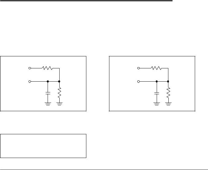
AC TEST CONDITIONS
Parameter |
Unit |
Input Pulse Level |
0 to 3V(1) |
Input Rise and Fall Times |
5 ns |
|
|
Input and Output Timing and Reference Level |
1.5V(1) |
Output Load |
See Figures 1 and 2 |
|
|
AC TEST LOADS
1076 Ω |
|
1076 Ω |
|
3V |
|
3V |
|
OUTPUT |
|
OUTPUT |
|
30 pF |
1262 Ω |
5 pF |
1262 Ω |
Including |
|
Including |
|
jig and |
|
jig and |
|
scope |
|
scope |
|
Figure 1. |
|
Figure 2. |
|
THEVENIN EQUIVALENT
581 Ω
OUTPUT 
 1.61V
1.61V
Figure 3.
Integrated Silicon Solution, Inc. — 1-800-379-4774 |
3 |
Rev. A
03/17/00

IS62V6416BLL |
|
|
ISSI® |
|
ABSOLUTE MAXIMUM RATINGS(1) |
|
|
|
|
|
|
|
|
|
Symbol Parameter |
Value |
Unit |
||
|
|
|
|
|
VTERM |
Terminal Voltage with Respect to GND |
–0.5 to Vcc +0.5 |
V |
|
|
|
|
|
|
TSTG |
Storage Temperature |
–65 to +150 |
°C |
|
|
|
|
|
|
PT |
Power Dissipation |
1.5 |
W |
|
|
|
|
|
|
IOUT |
DC Output Current (LOW) |
20 |
mA |
|
|
|
|
|
|
Note:
1.Stress greater than those listed under ABSOLUTE MAXIMUM RATINGS may cause permanent damage to the device. This is a stress rating only and functional operation of the device at these or any other conditions above those indicated in the operational sections of this specification is not implied. Exposure to absolute maximum rating conditions for extended periods may affect reliability.
OPERATING RANGE
Range |
Ambient Temperature |
VCC |
Commercial |
0°C to +70°C |
2.7V (Min.) to 3.3V (Max.) |
|
|
|
Industrial |
–40°C to +85°C |
2.7V (Min.) to 3.3V (Max.) |
|
|
|
DC ELECTRICAL CHARACTERISTICS (Over Operating Range Unless Otherwise Specified)
Symbol |
Parameter |
Test Conditions |
Min. |
Max. |
Unit |
VOH |
Output HIGH Voltage |
VCC = Min., IOH = –1 mA |
2.2 |
— |
V |
|
|
|
|
|
|
VOL |
Output LOW Voltage |
VCC = Min., IOL = 2.1 mA |
— |
0.4 |
V |
|
|
|
|
|
|
VIH |
Input HIGH Voltage |
|
2.0 |
VCC + 0.3 |
V |
|
|
|
|
|
|
VIL(1) |
Input LOW Voltage |
|
–0.2 |
0.4 |
V |
ILI |
Input Leakage |
GND ≤ VIN ≤ VCC |
–1 |
1 |
µA |
ILO |
Output Leakage |
GND ≤ VOUT ≤ VCC, Outputs Disabled |
–1 |
1 |
µA |
Note:
1. VIL (min.) = –1.5V for pulse width less than 30 ns.
4 Integrated Silicon Solution, Inc. — 1-800-379-4774
Rev. A
03/17/00
 Loading...