


ISSI IS61NW6432-6PQ, IS61NW6432-5TQ, IS61NW6432-5PQ, IS61NW6432-8TQ, IS61NW6432-8PQ Datasheet
...
|
IS61NW6432 |
|
|
ISSI |
|
|
|
|
|
|
|
|
® |
|
|
||
|
|
|
|
|
|
|
||
|
IS61NW6432 |
|
|
|
|
|
|
|
|
|
|
|
|
|
|
|
|
|
64K x 32 SYNCHRONOUS STATIC RAM |
ADVANCE INFORMATION |
||||||
WITH NO-WAIT STATE BUS FEATURE
JULY 1998
FEATURES
•Fast access time:
–5 ns-100 MHz; 6 ns-83 MHz;
–7 ns-75 MHz; 8 ns-66 MHz
•No wait cycles between Read and Write
•Internal self-timed write cycle
•Individual Byte Write Control
•Clock controlled, registered address, data and control
•Pentium™ or linear burst sequence control using MODE input
•Three chip enables for simple depth expansion and address pipelining
•Common data inputs and data outputs
•JEDEC 100-pin TQFP and PQFP package
•Single +3.3V power supply
•Optional data strobe pin (#80) for latching data (See page 12 for detailed timing)
DESCRIPTION
The IS61NW6432 is a high-speed, low-power synchronous static RAM designed to provide a burstable, highperformance, 'no-wait' bus, secondary cache for the Pentium, 680X0, and Power PC microprocessors. It is organized as 65,536 words by 32 bits, fabricated with ISSI's advanced CMOS technology.
Incorporating a 'no-wait' bus, wait cycles are eliminated when the bus switches from read to write, or write to read. This device integrates a 2-bit burst counter, high-speed SRAM core, and high-drive capability outputs into a single monolithic circuit.
All synchronous inputs pass through registers controlled by a positive-edge-triggered clock input. Operations may be suspended and all synchronous inputs ignored when Clock Enable, CEN is HIGH. In this state the internal device will hold their previous values.
When the ADV/LD is HIGH the internal burst counter is incremented. New external addresses can be loaded when ADV/LD is LOW.
Write cycles are internally self-timed and are initiated by the rising edge of the clock inputs and when RD/WE is LOW. Separate byte enables allow individual bytes to be written. BW1controls I/O1-I/O8; BW2controls I/O9-I/O16; BW3controls I/O17-I/O24; BW4 controls I/O25-I/O32. All Bytes are written when BW1, BW2, BW3, and BW4 are LOW.
MODE pin upon power up is in interleave burst mode. It can be connected to GNDQ or VCCQ to alter power up state.
This document contains ADVANCE INFORMATION data. ISSI reserves the right to make changes to its products at any time without notice in order to improve design and supply the best possible product. We assume no responsibility for any errors which may appear in this publication. © Copyright 1998, Integrated Silicon Solution, Inc.
Integrated Silicon Solution, Inc. |
1 |
ADVANCE INFORMATION SR050-0B 07/15/98

IS61NW6432
BLOCK DIAGRAM
MODE |
|
|
|
|
A0-A15 |
I |
|
O |
|
|
|
|
||
CE1, CE2, CE3 |
|
REGISTER |
|
|
R/W |
I |
O |
||
|
||||
CEN |
|
|
|
|
ADV/LD |
|
INPUT |
|
|
BW1 |
|
|
||
|
|
|
||
BW2 |
|
|
|
|
BW3 |
|
|
|
|
BW4 |
I |
|
O |
|
OE |
|
|
|
CLOCK
64K x 32 BIT MEMORY ARRAY
ADDRESS
CONTROL
DIN DOUT
CONTROL LOGIC
MUX
SEL
I
OUTPUT
REGISTER
O
GATE |
OE |
DATA DS
I/O1-I/O32 (Optional)
2 Integrated Silicon Solution, Inc.
ADVANCE INFORMATION SR050-0B 07/15/98
IS61NW6432
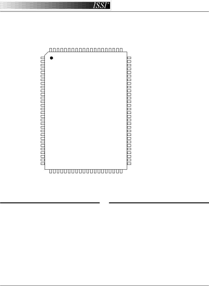
PIN CONFIGURATION
100-Pin TQFP and PQFP (Top View)
|
A6 |
A7 |
|
CE1 |
CE2 |
|
BW4 |
|
BW3 |
|
BW2 |
|
BW1 |
|
CE3 VCC |
GND CLK |
|
R/W |
|
CEN |
|
OE |
|
ADV/LD |
NC |
NC |
A8 |
A9 |
|
|
|
|
|
|
|
|
|
|
|
|
|
||||||||||||||||||
|
|
|
|
|
|
|
|
|
|
|
|
||||||||||||||||||
|
|
|
|
|
|
|
|
|
|
|
|||||||||||||||||||
|
|
|
|
|
|
|
|
|
|
||||||||||||||||||||
|
100 99 98 97 |
96 95 94 93 |
92 91 90 89 88 87 86 |
85 84 83 82 81 |
|
||||||||||||||||||||||||
NC |
1 |
|
|
|
|
|
|
|
|
|
|
|
|
|
|
|
|
|
|
|
|
|
|
|
|
|
|
80 |
NC |
I/O17 |
2 |
|
|
|
|
|
|
|
|
|
|
|
|
|
|
|
|
|
|
|
|
|
|
|
|
|
|
79 |
I/O16 |
I/O18 |
3 |
|
|
|
|
|
|
|
|
|
|
|
|
|
|
|
|
|
|
|
|
|
|
|
|
|
|
78 |
I/O15 |
VCCQ |
4 |
|
|
|
|
|
|
|
|
|
|
|
|
|
|
|
|
|
|
|
|
|
|
|
|
|
|
77 |
VCCQ |
GNDQ |
5 |
|
|
|
|
|
|
|
|
|
|
|
|
|
|
|
|
|
|
|
|
|
|
|
|
|
|
76 |
GNDQ |
I/O19 |
6 |
|
|
|
|
|
|
|
|
|
|
|
|
|
|
|
|
|
|
|
|
|
|
|
|
|
|
75 |
I/O14 |
I/O20 |
7 |
|
|
|
|
|
|
|
|
|
|
|
|
|
|
|
|
|
|
|
|
|
|
|
|
|
|
74 |
I/O13 |
I/O21 |
8 |
|
|
|
|
|
|
|
|
|
|
|
|
|
|
|
|
|
|
|
|
|
|
|
|
|
|
73 |
I/O12 |
I/O22 |
9 |
|
|
|
|
|
|
|
|
|
|
|
|
|
|
|
|
|
|
|
|
|
|
|
|
|
|
72 |
I/O11 |
GNDQ |
10 |
|
|
|
|
|
|
|
|
|
|
|
|
|
|
|
|
|
|
|
|
|
|
|
|
|
|
71 |
GNDQ |
VCCQ |
11 |
|
|
|
|
|
|
|
|
|
|
|
|
|
|
|
|
|
|
|
|
|
|
|
|
|
|
70 |
VCCQ |
I/O23 |
12 |
|
|
|
|
|
|
|
|
|
|
|
|
|
|
|
|
|
|
|
|
|
|
|
|
|
|
69 |
I/O10 |
I/O24 |
13 |
|
|
|
|
|
|
|
|
|
|
|
|
|
|
|
|
|
|
|
|
|
|
|
|
|
|
68 |
I/O9 |
VCC |
14 |
|
|
|
|
|
|
|
|
|
|
|
|
|
|
|
|
|
|
|
|
|
|
|
|
|
|
67 |
GND |
VCC |
15 |
|
|
|
|
|
|
|
|
|
|
|
|
|
|
|
|
|
|
|
|
|
|
|
|
|
|
66 |
VCC |
VCC |
16 |
|
|
|
|
|
|
|
|
|
|
|
|
|
|
|
|
|
|
|
|
|
|
|
|
|
|
65 |
VCC |
GND |
17 |
|
|
|
|
|
|
|
|
|
|
|
|
|
|
|
|
|
|
|
|
|
|
|
|
|
|
64 |
GND |
I/O25 |
18 |
|
|
|
|
|
|
|
|
|
|
|
|
|
|
|
|
|
|
|
|
|
|
|
|
|
|
63 |
I/O8 |
I/O26 |
19 |
|
|
|
|
|
|
|
|
|
|
|
|
|
|
|
|
|
|
|
|
|
|
|
|
|
|
62 |
I/O7 |
VCCQ |
20 |
|
|
|
|
|
|
|
|
|
|
|
|
|
|
|
|
|
|
|
|
|
|
|
|
|
|
61 |
VCCQ |
GNDQ |
21 |
|
|
|
|
|
|
|
|
|
|
|
|
|
|
|
|
|
|
|
|
|
|
|
|
|
|
60 |
GNDQ |
I/O27 |
22 |
|
|
|
|
|
|
|
|
|
|
|
|
|
|
|
|
|
|
|
|
|
|
|
|
|
|
59 |
I/O6 |
I/O28 |
23 |
|
|
|
|
|
|
|
|
|
|
|
|
|
|
|
|
|
|
|
|
|
|
|
|
|
|
58 |
I/O5 |
I/O29 |
24 |
|
|
|
|
|
|
|
|
|
|
|
|
|
|
|
|
|
|
|
|
|
|
|
|
|
|
57 |
I/O4 |
I/O30 |
25 |
|
|
|
|
|
|
|
|
|
|
|
|
|
|
|
|
|
|
|
|
|
|
|
|
|
|
56 |
I/O3 |
GNDQ |
26 |
|
|
|
|
|
|
|
|
|
|
|
|
|
|
|
|
|
|
|
|
|
|
|
|
|
|
55 |
GNDQ |
VCCQ |
27 |
|
|
|
|
|
|
|
|
|
|
|
|
|
|
|
|
|
|
|
|
|
|
|
|
|
|
54 |
VCCQ |
I/O31 |
28 |
|
|
|
|
|
|
|
|
|
|
|
|
|
|
|
|
|
|
|
|
|
|
|
|
|
|
53 |
I/O2 |
I/O32 |
29 |
|
|
|
|
|
|
|
|
|
|
|
|
|
|
|
|
|
|
|
|
|
|
|
|
|
|
52 |
I/O1 |
NC |
30 |
|
|
|
|
|
|
|
|
|
|
|
|
|
|
|
|
|
|
|
|
|
|
|
|
|
|
51 |
NC |
|
31 32 33 |
34 35 36 37 38 39 40 |
41 42 43 44 45 46 47 48 49 50 |
|
|||||||||||||||||||||||||
|
MODE |
A5 A4 |
A3 |
|
A2 A1 A0 NC |
|
NC GND |
VCC NC NC A10 A11 |
|
A12 |
A13 |
A14 |
A15 |
NC |
|
||||||||||||||
|
|
|
|
|
|
|
|
|
|
|
|
|
|
|
|
|
|
|
|
|
|
|
|
|
|
|
|
|
|
PIN DESCRIPTIONS
A0-A15 |
Address Inputs |
|
|
CLK |
Clock |
|
|
CEN |
Clock Enable |
|
|
ADV/CD |
Advance Load |
|
|
BW1-BW4 |
Synchronous Byte Write Enable |
|
|
R/W |
Read/Write |
|
|
CE1, CE2, CE3 Synchronous Chip Enable |
|
|
|
OE |
Output Enable |
|
|
Note:
1. Optional, NC or DS.
DS(1) |
Data Strobe |
I/O1-I/O32 |
Data Input/Output |
|
|
MODE |
Burst Sequence Mode |
|
|
VCC |
+3.3V Power Supply |
|
|
GND |
Ground |
|
|
VCCQ |
Isolated Output Buffer Supply: +3.3V |
|
|
GNDQ |
Isolated Output Buffer Ground |
|
|
NC |
No Connect |
|
|
Integrated Silicon Solution, Inc. |
3 |
ADVANCE INFORMATION SR050-0B 07/15/98
IS61NW6432
TRUTH TABLE(1)
|
Address |
|
|
|
|
|
|
Operation |
Used |
R/W |
CEx |
ADV/LD |
CEN |
BWx |
CLK |
|
|
|
|
|
|
|
|
Begin New Write Cycle |
External |
L |
L |
L |
L |
Valid |
L-H |
|
|
|
|
|
|
|
|
Begin New Read Cycle |
External |
H |
L |
L |
L |
X |
L-H |
|
|
|
|
|
|
|
|
Advance Burst Counter(2) |
Internal |
X |
X |
H |
L |
Valid |
L-H |
(Burst Write) |
|
|
|
|
|
|
|
Advance Burst Counter |
Internal |
X |
X |
H |
L |
X |
L-H |
(Burst Read) |
|
|
|
|
|
|
|
|
|
|
|
|
|
|
|
Deselect (2 Cycle)(3) |
X |
X |
H |
L |
L |
X |
L-H |
Hold/NOOP(4) |
X |
X |
X |
X |
H |
X |
L-H |
Notes: |
|
|
|
|
|
|
|
1."X" Means don't care.
2.When ADV/LD signal is sampled HIGH, the internal burst counter is incremented. The R/W signal is ignored when the counter is advanced. Therefore, the nature of the burst cycle (Read or Write) is determined by the status of the R/W signal when the first address is loaded at the beginning of the burst cycle.
3.Deselect cycle is initiated when CEx is sampled HIGH and ADV/LD sampled LOW at rising edge of clock. The data bus will tri-state two cycles after deselect is initiated.
4.When CEN is sampled high at the rising edge of clock, that clock edge is blocked from propogating through the part. The state of all the internal registers remains unchanged.
PARTIAL TRUTH TABLE (Non-burst)
Function |
R/W |
BW1 |
BW2 |
BW3 |
BW4 |
CEx |
ADV/LD |
Read |
H |
X |
X |
X |
X |
L |
L |
|
|
|
|
|
|
|
|
Write Byte 1 |
L |
L |
H |
H |
H |
L |
L |
|
|
|
|
|
|
|
|
Write Byte 2 |
L |
H |
L |
H |
H |
L |
L |
Write Byte 3 |
L |
H |
H |
L |
H |
L |
L |
|
|
|
|
|
|
|
|
Write Byte 4 |
L |
H |
H |
H |
L |
L |
L |
|
|
|
|
|
|
|
|
Write All Bytes |
L |
L |
L |
L |
L |
L |
L |
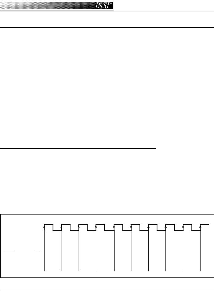
FUNCTIONAL TIMING DIAGRAM
CYCLE |
n+29 |
n+30 |
n+31 |
n+32 |
n+33 |
n+34 |
n+35 |
n+36 |
n+37 |
|
CLOCK |
|
|
|
|
|
|
|
|
|
|
ADDRESS |
A29 |
A30 |
A31 |
A32 |
A33 |
A34 |
A35 |
A36 |
A37 |
|
(A0-A15) |
|
|
|
|
|
|
|
|
|
|
CONTROL |
C29 |
C30 |
C31 |
C32 |
C33 |
C34 |
C35 |
C36 |
C37 |
|
(BWx, R/W, ADV/LD) |
||||||||||
|
|
|
|
|
|
|
|
|
||
DATA |
D27 |
D28 |
D29 |
D30 |
D31 |
D32 |
D33 |
D34 |
D35 |
|
(I/O1-I/O32) |
||||||||||
|
|
|
|
|
|
|
|
|
4 |
Integrated Silicon Solution, Inc. |
ADVANCE INFORMATION SR050-0B 07/15/98
 Loading...