


ISSI IS61NSCS51236-333B, IS61NSCS51236-300B, IS61NSCS25672-300B, IS61NSCS25672-250B, IS61NSCS51236-250B Datasheet
...
|
IS61NSCS25672 |
® |
|
IS61NSCS51236 |
ISSI |
|
ΣRAM 256K x 72, 512K x 36 |
JUNE 2001 |
|
|
ADVANCE INFORMATION |
|
18Mb Synchronous SRAM |
|
Features
•JEDEC SigmaRam pinout and package standard
•Single 1.8V power supply (VCC): 1.7V (min) to 1.9V (max)
•Dedicated output supply voltage (VCCQ): 1.8V or 1.5V typical
•LVCMOS-compatible I/O interface
•Common data I/O pins (DQs)
•Single Data Rate (SDR) data transfers
•Pipelined (PL) read operations
•Double Late Write (DLW) write operations
•Burst and non-burst read and write operations, selectable via dedicated control pin (ADV)
•Internally controlled Linear Burst address sequencing during burst operations
•Burst length of 2, 3, or 4, with automatic address wrap
•Full read/write coherency
•Byte write capability
Bottom View
209-Bump, 14 mm x 22 mm BGA
1 mm Bump Pitch, 11 x 19 Bump Array
•Two cycle deselect
•Single-ended input clock (CLK)
•Data-referenced output clocks (CQ/CQ)
•Selectable output driver impedance via dedicated control pin (ZQ)
•Echo clock outputs track data output drivers
•Depth expansion capability (2 or 4 banks) via programmable chip enables (E2, E3, EP2, EP3)
•JTAG boundary scan (subset of IEEE standard 1149.1)
•209 pin (11x19), 1mm pitch, 14mm x 22mm Ball Grid Array (BGA) package
SigmaRAM Family Overview
The IS61NSCS series ΣRAMs are built in compliance with the SigmaRAM pinout standard for synchronous SRAMs. The implementations are 18,874,368-bit (18Mb) SRAMs. These are the first in a family of wide, very low voltage CMOS I/O SRAMs designed to operate at the speeds needed to implement economical high performance networking systems.
ISSI’s ΣRAMs are offered in a number of configurations that emulate other synchronous SRAMs, such as Burst RAMs, NBT RAMs, Late Write, or Double Data Rate (DDR) SRAMs. The logical differences between the protocols employed by these RAMs hinge mainly on various combinations of address bursting, output data registering and write cueing. ΣRAMs allow a user to implement the interface protocol best suited to the task at hand.
This specific product is Common I/O, SDR, Double Late Write & Pipelined Read (same as Pipelined NBT) and in the family is identified as 1x1Dp.
This document contains ADVANCE INFORMATION data. ISSI reserves the right to make changes to its products at any time without notice in order to improve design and supply the best possible product. We assume no responsibility for any errors which may appear in this publication. © Copyright 2001, Integrated Silicon Solution, Inc.
Integrated Silicon Solution, Inc. — 1-800-379-4774 |
1 |
ADVANCE INFORMATION Rev. 00A
06/19/01
IS61NSCS25672 |
ISSI |
® |
IS61NSCS51236 |
|
Functional Description
Because SigmaRAM is a synchronous device, address, data Inputs, and read/write control inputs are captured on the rising edge of the input clock. Write cycles are internally self-timed and initiated by the rising edge of the clock input. This feature eliminates complex off-chip write pulse generation required by asynchronous SRAMs and simplifies input signal timing.
Single data rate ΣRAMs incorporate a rising-edge-triggered output register. For read cycles, ΣRAM’s output data is temporarily stored by the edge-triggered output register during the access cycle and then released to the output drivers at the next rising edge of clock.
IS61NSCS series ΣRAMs are implemented with ISSI’s high performance CMOS technology and are packaged in a 209-bump BGA.
IS61NSCS25672 PINOUT
256K x 72 Common I/O—Top View
|
1 |
2 |
3 |
4 |
5 |
6 |
7 |
8 |
9 |
10 |
|
11 |
|
A |
|
|
|
|
|
|
|
|
|
|
|
|
|
DQg |
DQg |
A |
E2 |
A |
ADV |
|
A |
E3 |
A |
DQb |
|
DQb |
|
|
|
|
|
|
(16M) |
|
|
(8M) |
|
|
|
|
|
|
|
|
|
|
|
|
|
|
|
|
|
|
|
B |
DQg |
DQg |
Bc |
Bg |
NC |
W |
|
A |
Bb |
Bf |
DQb |
|
DQb |
|
|
|
|
|
|
|
|
|
|
|
|
|
|
C |
DQg |
DQg |
Bh |
Bd |
NC |
E1 |
|
NC |
Be |
Ba |
DQb |
|
DQb |
|
|
|
|
|
(128M) |
|
|
|
|
|
|
|
|
|
|
|
|
|
|
|
|
|
|
|
|
|
|
D |
DQg |
DQg |
GND |
NC |
NC |
MCL |
|
NC |
NC |
GND |
DQb |
|
DQb |
|
|
|
|
|
|
|
|
|
|
|
|
|
|
E |
DQPg |
DQPc |
VCCQ |
VCCQ |
VCC |
VCC |
|
VCC |
VCCQ |
VCCQ |
DQPf |
|
DQPb |
|
|
|
|
|
|
|
|
|
|
|
|
|
|
F |
DQc |
DQc |
GND |
GND |
GND |
ZQ |
|
GND |
GND |
GND |
DQf |
|
DQf |
|
|
|
|
|
|
|
|
|
|
|
|
|
|
G |
DQc |
DQc |
VCCQ |
VCCQ |
VCC |
EP2 |
|
VCC |
VCCQ |
VCCQ |
DQf |
|
DQf |
|
|
|
|
|
|
|
|
|
|
|
|
|
|
H |
DQc |
DQc |
GND |
GND |
GND |
EP3 |
|
GND |
GND |
GND |
DQf |
|
DQf |
|
|
|
|
|
|
|
|
|
|
|
|
|
|
J |
DQc |
DQc |
VCCQ |
VCCQ |
VCC |
M4 |
|
VCC |
VCCQ |
VCCQ |
DQf |
|
DQf |
|
|
|
|
|
|
|
|
|
|
|
|
|
|
K |
CQ2 |
CQ2 |
CLK |
NC |
GND |
MCL |
|
GND |
NC |
NC |
CQ1 |
|
CQ1 |
|
|
|
|
|
|
|
|
|
|
|
|
|
|
L |
DQh |
DQh |
VCCQ |
VCCQ |
VCC |
M2 |
|
VCC |
VCCQ |
VCCQ |
DQa |
|
DQa |
|
|
|
|
|
|
|
|
|
|
|
|
|
|
M |
DQh |
DQh |
GND |
GND |
GND |
M3 |
|
GND |
GND |
GND |
DQa |
|
DQa |
|
|
|
|
|
|
|
|
|
|
|
|
|
|
N |
DQh |
DQh |
VCCQ |
VCCQ |
VCC |
SD |
|
VCC |
VCCQ |
VCCQ |
DQa |
|
DQa |
|
|
|
|
|
|
|
|
|
|
|
|
|
|
P |
DQh |
DQh |
GND |
GND |
GND |
MCL |
|
GND |
GND |
GND |
DQa |
|
DQa |
|
|
|
|
|
|
|
|
|
|
|
|
|
|
R |
DQPd |
DQPh |
VCCQ |
VCCQ |
VCC |
VCC |
|
VCC |
VCCQ |
VCCQ |
DQPa |
|
DQPe |
|
|
|
|
|
|
|
|
|
|
|
|
|
|
T |
DQd |
DQd |
GND |
NC |
NC |
MCL |
|
NC |
NC |
GND |
DQe |
|
DQe |
|
|
|
|
|
|
|
|
|
|
|
|
|
|
U |
DQd |
DQd |
NC |
A |
NC |
A |
|
NC |
A |
NC |
DQe |
|
DQe |
|
|
|
|
|
(64M) |
|
|
(32M) |
|
|
|
|
|
|
|
|
|
|
|
|
|
|
|
|
|
|
|
V |
DQd |
DQd |
A |
A |
A |
A1 |
|
A |
A |
A |
DQe |
|
DQe |
|
|
|
|
|
|
|
|
|
|
|
|
|
|
W |
DQd |
DQd |
TMS |
TDI |
A |
A0 |
|
A |
TDO |
TCK |
DQe |
|
DQe |
|
|
|
|
|
|
|
|
|
|
|
|
|
|
11 x 19 Bump BGA—14 x 22 mm2 Body—1 mm Bump Pitch |
|
|
|
|
|
|
|
||||||
|
|
|
|
|
|
|
|
|
|
|
|
|
|
2 |
|
|
|
|
|
|
Integrated Silicon Solution, Inc. — 1-800-379-4774 |
||||||
|
|
|
|
|
|
|
|
|
|
ADVANCE INFORMATION |
Rev. 00A |
||
|
|
|
|
|
|
|
|
|
|
|
|
|
06/19/01 |

IS61NSCS25672 |
|
|
|
|
|
|
|
ISSI |
® |
|||
IS61NSCS51236 |
|
|
|
|
|
|
|
|
||||
IS61NSCS51236 PINOUT |
|
|
|
|
|
|
|
|
|
|||
512K x 36 Common I/O—Top View |
|
|
|
|
|
|
|
|
||||
|
1 |
2 |
3 |
4 |
5 |
6 |
7 |
8 |
9 |
10 |
11 |
|
A |
|
|
|
|
|
|
|
|
|
|
|
|
NC |
NC |
A |
E2 |
A |
ADV |
A |
E3 |
A |
DQb |
DQb |
|
|
|
|
|
|
|
(16M) |
|
|
|
|
|
|
|
|
|
|
|
|
|
|
|
|
|
|
|
|
B |
NC |
NC |
Bc |
NC |
A |
W |
A |
Bb |
NC |
DQb |
DQb |
|
|
|
|
|
|
(x36) |
|
|
|
|
|
|
|
|
|
|
|
|
|
|
|
|
|
|
|
|
C |
NC |
NC |
NC |
Bd |
NC |
E1 |
NC |
NC |
Ba |
DQb |
DQb |
|
|
|
|
|
|
(128M) |
|
|
|
|
|
|
|
|
|
|
|
|
|
|
|
|
|
|
|
|
D |
NC |
NC |
GND |
NC |
NC |
MCL |
NC |
NC |
GND |
DQb |
DQb |
|
|
|
|
|
|
|
|
|
|
|
|
|
|
E |
NC |
DQPc |
VCCQ |
VCCQ |
VCC |
VCC |
VCC |
VCCQ |
VCCQ |
NC |
DQPb |
|
|
|
|
|
|
|
|
|
|
|
|
|
|
F |
DQc |
DQc |
GND |
GND |
GND |
ZQ |
GND |
GND |
GND |
NC |
NC |
|
|
|
|
|
|
|
|
|
|
|
|
|
|
G |
DQc |
DQc |
VCCQ |
VCCQ |
VCC |
EP2 |
VCC |
VCCQ |
VCCQ |
NC |
NC |
|
|
|
|
|
|
|
|
|
|
|
|
|
|
H |
DQc |
DQc |
GND |
GND |
GND |
EP3 |
GND |
GND |
GND |
NC |
NC |
|
|
|
|
|
|
|
|
|
|
|
|
|
|
J |
DQc |
DQc |
VCCQ |
VCCQ |
VCC |
M4 |
VCC |
VCCQ |
VCCQ |
NC |
NC |
|
|
|
|
|
|
|
|
|
|
|
|
|
|
K |
CQ2 |
CQ2 |
CLK |
NC |
GND |
MCL |
GND |
NC |
NC |
CQ1 |
CQ1 |
|
|
|
|
|
|
|
|
|
|
|
|
|
|
L |
NC |
NC |
VCCQ |
VCCQ |
VCC |
M2 |
VCC |
VCCQ |
VCCQ |
DQa |
DQa |
|
|
|
|
|
|
|
|
|
|
|
|
|
|
M |
NC |
NC |
GND |
GND |
GND |
M3 |
GND |
GND |
GND |
DQa |
DQa |
|
|
|
|
|
|
|
|
|
|
|
|
|
|
N |
NC |
NC |
VCCQ |
VCCQ |
VCC |
SD |
VCC |
VCCQ |
VCCQ |
DQa |
DQa |
|
|
|
|
|
|
|
|
|
|
|
|
|
|
P |
NC |
NC |
GND |
GND |
GND |
MCL |
GND |
GND |
GND |
DQa |
DQa |
|
|
|
|
|
|
|
|
|
|
|
|
|
|
R |
DQPd |
NC |
VCCQ |
VCCQ |
VCC |
VCC |
VCC |
VCCQ |
VCCQ |
DQPa |
NC |
|
|
|
|
|
|
|
|
|
|
|
|
|
|
T |
DQd |
DQd |
GND |
NC |
NC |
MCL |
NC |
NC |
GND |
NC |
NC |
|
|
|
|
|
|
|
|
|
|
|
|
|
|
U |
DQd |
DQd |
NC |
A |
NC |
A |
NC |
A |
NC |
NC |
NC |
|
|
|
|
|
|
(64M) |
|
(32M) |
|
|
|
|
|
|
|
|
|
|
|
|
|
|
|
|
|
|
V |
DQd |
DQd |
A |
A |
A |
A1 |
A |
A |
A |
NC |
NC |
|
|
|
|
|
|
|
|
|
|
|
|
|
|
W |
DQd |
DQd |
TMS |
TDI |
A |
A0 |
A |
TDO |
TCK |
NC |
NC |
|
|
|
|
|
|
|
|
|
|
|
|
|
|
11 x 19 Bump BGA—14 x 22 mm2 Body—1 mm Bump Pitch
Integrated Silicon Solution, Inc. — 1-800-379-4774 |
3 |
ADVANCE INFORMATION Rev. 00A
06/19/01

IS61NSCS25672 |
|
|
ISSI |
® |
|
IS61NSCS51236 |
|
|
|
||
PIN DESCRIPTION TABLE |
|
|
|
|
|
|
|
|
|
|
|
Symbol |
Pin Location |
Description |
Type |
Comments |
|
|
|
|
|
|
|
A |
A3, A5, A7, A9, B7, U4, |
Address |
Input |
— |
|
|
U6, U8, V3, V4, V5, V6, |
|
|
|
|
|
V7, V8, V9, W5, W6, W7 |
|
|
|
|
|
|
|
|
|
|
A |
B5 |
Address |
Input |
x36version |
|
|
|
|
|
|
|
ADV |
A6 |
Advance |
Input |
Active High |
|
|
|
|
|
|
|
Bx |
B3, C9 |
Byte Write Enable |
Input |
Active Low (all versions) |
|
|
|
|
|
|
|
Bx |
B8, C4 |
Byte Write Enable |
Input |
Active Low (x36 and x72 versions) |
|
|
|
|
|
|
|
Bx |
B4, B9, C3, C8 |
Byte Write Enable |
Input |
Active Low (x72 version only) |
|
|
|
|
|
|
|
CK |
K3 |
Clock |
Input |
Active High |
|
|
|
|
|
|
|
CQ |
K1, K11 |
Echo Clock |
Output |
Active High |
|
|
|
|
|
|
|
CQ |
K2, K10 |
Echo Clock |
Output |
Active Low |
|
|
|
|
|
|
|
DQ |
E2, F1, F2, G1, G2, H1, |
Data I/O |
Input/Output |
x36, and x72 versions |
|
|
H2, J1, J2, L10, L11, |
|
|
|
|
|
M10, M11, N10, N11, |
|
|
|
|
|
P10, P11, R10 |
|
|
|
|
|
A10, A11, B10, B11, |
Data I/O |
Input/Output |
|
|
|
C10, C11, D10, D11, |
|
|
|
|
|
E11, R1, T1, T2, U1, U2, |
|
|
|
|
|
V1, V2, W1, W2 |
|
|
|
|
|
|
|
|
|
|
DQ |
A1, A2, B1, B2, C1, C2, |
Data I/O |
Input/Output |
x72 version only |
|
|
D1, D2, E1, E10, F10, |
|
|
|
|
|
F11, G10, G11, H10, |
|
|
|
|
|
H11, J10, J11, L1, L2, |
|
|
|
|
|
M1, M2, N1, N2, P1, P2, |
|
|
|
|
|
R2, R11, T10, T11, U10, |
|
|
|
|
|
U11, V10, V11, W10, |
|
|
|
|
|
W11 |
|
|
|
|
|
|
|
|
|
|
E1 |
C6 |
Chip Enable |
Input |
Active Low |
|
|
|
|
|
|
|
E2 & E3 |
A4, A8 |
Chip Enable |
Input |
Programmable Active High or Low |
|
|
|
|
|
|
|
EP2 & EP3 |
G6, H6 |
Chip Enable Program Pin |
Input |
— |
|
|
|
|
|
|
|
TCK |
W9 |
Test Clock |
Input |
Active High |
|
|
|
|
|
|
|
TDI |
W4 |
Test Data In |
Input |
— |
|
|
|
|
|
|
|
TDO |
W8 |
Test Data Out |
Output |
— |
|
|
|
|
|
|
|
TMS |
W3 |
Test Mode Select |
Input |
— |
|
|
|
|
|
|
|
M2, M3 & M4 |
L6, M6, J6 |
Mode Control Pins |
Input |
— |
|
|
|
|
|
|
|
SD |
N6 |
Slow Down |
Input |
Active Low |
|
|
|
|
|
|
|
MCL |
B3, C9, D6, K6 |
Must Connect Low |
Input |
— |
|
|
P6, T6, W6 |
|
|
|
|
|
|
|
|
|
|
4 Integrated Silicon Solution, Inc. — 1-800-379-4774
ADVANCE INFORMATION Rev. 00A
06/19/01

IS61NSCS25672 |
|
|
|
ISSI |
® |
IS61NSCS51236 |
|
|
|
|
|
PIN DESCRIPTION TABLE |
|
|
|
|
|
|
|
|
|
|
|
Symbol |
Pin Location |
Description |
Type |
Comments |
|
|
|
|
|
|
|
|
C5, D4, D5, D7, D8, K4, |
|
|
|
|
NC |
K8, K9, T4, T5, T7, |
NoConnect |
— |
Not connected to die (all versions) |
|
|
T8, U3, U5, U7, U9 |
|
|
|
|
|
|
|
|
|
|
NC |
B5 |
NoConnect |
— |
Not connected to die (x72 version) |
|
|
|
|
|
|
|
NC |
C7 |
NoConnect |
— |
Not connected to die (x72/x36 versions) |
|
|
|
|
|
|
|
|
A1, A2, B1, B2, B4, B9, |
|
|
|
|
|
C1, C2, C3, C8, D1, D2, |
|
|
|
|
|
E1, E10, F10, F11, G10, |
|
|
|
|
NC |
G11, H10, H11, J10, J11, |
NoConnect |
— |
Not connected to die (x36 version) |
|
|
L1, L2, M1, M2, N1, N2, |
|
|
|
|
|
P1, P2, R2, R11, T10, |
|
|
|
|
|
T11, U10, U11, V10, |
|
|
|
|
|
V11, W10, W11 |
|
|
|
|
|
|
|
|
|
|
W |
B6 |
Write |
Input |
Active Low |
|
|
|
|
|
|
|
|
E5, E6, E7, G5, G7, |
|
|
|
|
VCC |
J5, J7, L5, L7, N5, |
CorePowerSupply |
Input |
1.8 V Nominal |
|
|
N7, R5, R6, R7 |
|
|
|
|
|
|
|
|
|
|
|
E3, E4, E8, E9, J3, J4, |
|
|
|
|
VCCQ |
J8, J9, L3, L4, L8, |
Output Driver Power Supply |
Input |
1.8 V or 1.5 V Nominal |
|
|
L9, N3, N4, N8, N9, |
|
|
|
|
|
R3, R4, R8, R9 |
|
|
|
|
|
|
|
|
|
|
|
D3, D9, F3, F4, F5, F7, |
|
|
|
|
|
F8, F9, H3, H4, H5, H7, |
|
|
|
|
GND |
H8, H9, K5, K7, M3, M4, |
Ground |
Input |
— |
|
|
M5, M7, M8, M9, P3, P4, |
|
|
|
|
|
P5, P7, P8, P9, T3, T9 |
|
|
|
|
|
|
|
|
|
|
ZQ |
F6 |
OutputImpedanceControl |
Input |
Low = Low Impedance [High Drive] |
|
|
|
|
|
High = High Impedance [Low Drive] |
|
|
|
|
|
Default = High |
|
|
|
|
|
|
|
Integrated Silicon Solution, Inc. — 1-800-379-4774 |
5 |
ADVANCE INFORMATION Rev. 00A
06/19/01
IS61NSCS25672 |
ISSI |
® |
IS61NSCS51236 |
|
BACKGROUND
The central characteristics of the ISSI ΣRAMs are that they are extremely fast and consume very little power. Because both operating and interface power is low, ΣRAMs can be implemented in a wide (x72) configuration, providing very high single package bandwidth (in excess of 20 Gb/s in ordinary pipelined configuration) and very low random access latency (5 ns). The use of very low voltage circuits in the core and 1.8V or 1.5V interface voltages allow the speed, power and density performance of ΣRAMs.
Although the SigmaRAM family pinouts have been designed to support a number of different common read and write protocol options, not all SigmaRAM implementations will support all possible protocols. The following timing diagrams provide a quick comparison between read and write protocols options available in the context of the SigmaRAM
standard. This data sheet covers the single data rate (nonDDR), Double Late Write, Pipelined Read SigmaRAM.
The character of the applications for fast synchronous SRAMs in networking systems are extremely diverse. ΣRAMs have been developed to address the diverse needs of the networking market in a manner that can be supported with a unified development and manufacturing infrastructure. ΣRAMs address each of the bus protocol options commonly found in networking systems. This allows the ΣRAM to find application in radical shrinks and speed-ups of existing networking chip sets that were designed for use with older SRAMs, like the NBT or Nt, Late Write, or Double Data Rate SRAMs, as well as with new chip sets and ASIC’s that employ the Echo Clocks and realize the full potential of the ΣRAMs.
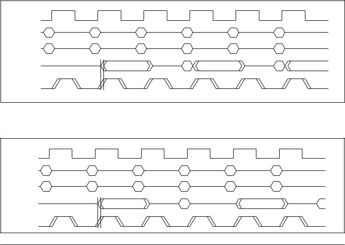
COMMON I/O SigmaRAM FAMILY MODE COMPARISON—LATE WRITE VS. DOUBLE LATE WRITE
Double Late Write—Pipelined Read (Σ1x1Dp). For reference only.
CK |
|
|
|
|
|
|
|
Address |
A |
B |
C |
D |
E |
F |
|
Control |
R |
W |
R |
W |
R |
W |
|
DQ |
|
|
QA |
DB |
QC |
DD |
QE |
CQ |
|
|
|
|
|
|
|
Late Write—Pipelined Read (Σ1x1Lp). For reference only.
CK |
|
|
|
|
|
|
|
Address |
A |
B |
C |
D |
E |
F |
|
Control |
R |
X |
W |
R |
X |
W |
|
DQ |
|
|
QA |
DC |
QD |
DF |
|
CQ |
|
|
|
|
|
|
|
6 |
|
|
|
Integrated Silicon Solution, Inc. — 1-800-379-4774 |
|||
|
|
|
|
|
ADVANCE INFORMATION |
Rev. 00A |
|
|
|
|
|
|
|
|
06/19/01 |
IS61NSCS25672 |
ISSI |
® |
IS61NSCS51236 |
|
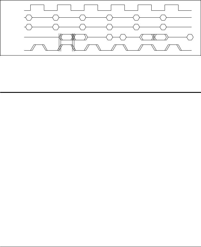
Double Data Rate Write—Double Data Rate Read (Σ1x2Lp). For reference only.
CK |
|
|
|
|
|
|
|
|
Address |
A |
B |
C |
D |
E |
|
F |
|
Control |
R |
X |
W |
R |
X |
|
W |
|
DQ |
|
QA0 |
QA1 |
DC0 |
DC1 |
QD0 |
QD1 |
DF0 |
CQ |
|
|
|
|
|
|
|
|
Mode Selection Truth Table Standard
Name |
M2 |
M3 |
M4 |
Function |
Analogous to... |
In This Data Sheet? |
Σ1x2Lp |
0 |
1 |
1 |
DDR |
Double Data Rate SRAM |
No |
|
|
|
|
|
|
|
Σ1x1Dp |
1 |
0 |
1 |
Double Late Write, Pipelined Read |
Pipelined NBT SRAM |
Yes |
|
|
|
|
|
|
|
Σ1x1Lp |
1 |
1 |
0 |
Late Write, Pipelined Read |
Pipelined Late Write SRAM |
No |
Notes:
All address, data and control inputs (with the exception of EP2, EP3, and the mode pins, M2–M4) are synchronized to rising clock edges. Read and write operations must be initiated with the Advance/Load pin (ADV) held low, in order to load the new address. Device activation is accomplished by asserting all three of the Chip Enable inputs (E1, E2, and E3). Deassertion of any one of the Enable inputs will deactivate the device. It should be noted that ONLY deactivation of the RAM via E2 and/or E3 deactivates the Echo Clocks, CQ1–CQn.
READ OPERATIONS
Pipelined Read
Read operation is initiated when the following conditions are satisfied at the rising edge of clock: All three chip enables (E1, E2, and E3) are active, the write enable input signal (W) is deasserted high, and ADV is asserted low. The address presented to the address inputs is latched into the address register and presented to the memory core and control logic. The control logic determines that a read access is in progress and allows the requested data to propagate to the input of the output register. At the next rising edge of clock the read data is allowed to propagate through the output register and onto the output pins.
WRITE OPERATIONS
Write operation occurs when the following conditions are satisfied at the rising edge of clock: All three chip enables (E1, E2, and E3) are active and the write enable input signal (W) is asserted low.
Double Late Write
Double Late Write means that Data In is required on the third rising edge of clock. Double Late Write is used to implement Pipeline mode NBT SRAMs.
Integrated Silicon Solution, Inc. — 1-800-379-4774 |
7 |
ADVANCE INFORMATION Rev. 00A
06/19/01

IS61NSCS25672 |
ISSI |
® |
IS61NSCS51236 |
|
|
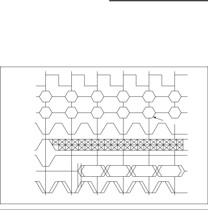
Single Data Rate Pipelined Read |
|
|
CLK
Address |
A |
XX |
C |
E1
W |
|
DQ |
QA |
CQ |
|
D E F
QC |
QD |
Read |
Deselect |
Read |
Read |
Read |
Double Late Write with Pipelined Read
CLK |
|
|
|
|
|
|
|
Address |
A |
B |
C |
D |
E |
F |
|
E1 |
|
|
|
|
|
|
|
W |
|
|
|
|
|
|
|
DQ |
|
|
QA |
DB |
QC |
DD |
|
CQ |
|
|
|
|
|
|
|
|
Read |
Write |
Read |
Write |
Read |
Write |
|
8 |
|
|
|
Integrated Silicon Solution, Inc. — 1-800-379-4774 |
|||
|
|
|
|
|
|
ADVANCE INFORMATION |
Rev. 00A |
|
|
|
|
|
|
|
06/19/01 |
IS61NSCS25672 |
ISSI |
® |
IS61NSCS51236 |
|
SPECIAL FUNCTIONS
Slow Down Mode
The SD pin allows the user to activate a delay element in the on-chip clock chain that is routed to the data and echo Clock output drivers. Activating Slow Down mode by pulling the SD pin low introduces extra delay in every synchronous output driver specification. Address, control and data input specifications are not affected by Slow Down Mode. See “Slow Down Mode Clock to Data Out and Clock to Echo Clock Timing” table for specifics.
Burst Cycles
ΣRAMs provide an on-chip burst address generator that can be utilized, if desired, to further simplify burst read or write implementations. The ADV control pin, when driven high, commands the ΣRAM to advance the internal address counter and use the counter generated address to read or write the ΣRAM. The starting address for the first cycle in a burst cycle series is loaded into the ΣRAM by driving the ADV pin low, into Load mode.
Burst Order
The burst address counter wraps around to its initial state after four addresses (the loaded address and three more) have been accessed. SigmaRAMs always count in linear burst order.
Linear Burst Order
|
A[1:0] |
A[1:0] |
A[1:0] |
A[1:0] |
1st address |
00 |
01 |
10 |
11 |
|
|
|
|
|
2nd address |
01 |
10 |
11 |
00 |
|
|
|
|
|
3rd address |
10 |
11 |
00 |
01 |
|
|
|
|
|
4th address |
11 |
00 |
01 |
10 |
|
|
|
|
|
Note:
1.The burst counter wraps to initial state on the 5th rising edge of clock.
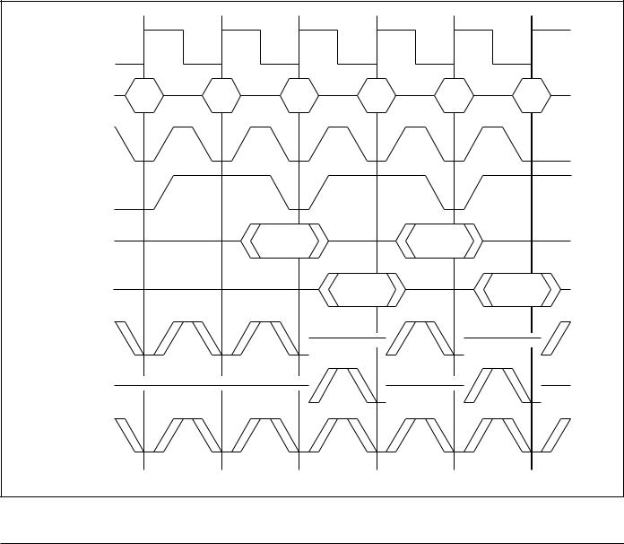
Sigma Pipelined Burst Reads with Counter Wrap-around
CLK |
|
|
|
|
|
|
|
External |
A2 |
XX |
XX |
XX |
XX |
XX |
|
Address |
|||||||
|
|
|
|
|
|
||
Internal |
A2 |
A3 |
A0 |
A1 |
A2 |
A3 |
|
Address |
|||||||
|
|
|
|
|
|
||
|
|
|
|
|
|
Counter Wraps |
|
E1 |
|
|
|
|
|
|
W
ADV |
|
|
|
|
|
DQ |
|
QA2 |
QA3 |
QA0 |
QA1 |
CQ |
|
|
|
|
|
Read |
Continue |
Continue |
Continue |
Continue |
|
Integrated Silicon Solution, Inc. — 1-800-379-4774 |
9 |
ADVANCE INFORMATION Rev. 00A
06/19/01
IS61NSCS25672 |
ISSI |
® |
IS61NSCS51236 |
|
Echo Clock
ΣRAMs feature Echo Clocks, CQ1,CQ2, CQ1, and CQ2 that track the performance of the output drivers. The Echo Clocks are delayed copies of the main RAM clock, CLK. Echo Clocks are designed to track changes in output driver delays due to variance in die temperature and supply voltage. The Echo Clocks are designed to fire with the rest of the data output drivers. Sigma RAMs provide both in-phase, or true, Echo Clock outputs (CQ1 and CQ2) and inverted Echo Clock outputs (CQ1 and CQ2).
It should be noted that deselection of the RAM via E2 and E3 also deselects the Echo Clock output drivers. The deselection of Echo Clock drivers is always pipelined to
the same degree as output data. Deselection of the RAM via E1 does not deactivate the Echo Clocks.
In some applications it may be appropriate to pause between banks; to deselect both RAMs with E1 before resuming read operations. An E1 deselect at a bank switch will allow at least one clock to be issued from the new bank before the first read cycle in the bank. Although the following drawing illustrates a E1 read pause upon switching from Bank 1 to Bank 2, a write to Bank 2 would have the same effect, causing the RAM in Bank 2 to issue at least one clock before it is needed.
Echo Clock Control in Two Banks of Sigma Pipelined SRAMs
CLK |
|
|
|
|
|
|
Address |
A |
B |
C |
D |
E |
F |
E1 |
|
|
|
|
|
|
E2 Bank 1 |
|
|
|
|
|
|
E2 Bank 2 |
|
|
|
|
|
|
DQ Bank 1 |
|
|
QA |
|
QC |
|
DQ Bank 2 |
|
|
|
QB |
|
QD |
CQ Bank 1 |
|
|
|
|
|
|
CQ Bank 2 |
|
|
|
|
|
|
CQ1+ CQ2 |
|
|
|
|
|
|
|
Read |
Read |
Read |
Read |
Read |
Read |
Note:
E1 does not deselect the Echo Clock Outputs. Echo Clock outputs are synchronously deselected by E2 or E3 being sampled false.
10 Integrated Silicon Solution, Inc. — 1-800-379-4774
ADVANCE INFORMATION Rev. 00A
06/19/01
 Loading...