


IS61NLF51218-10TQI
ISSI IS61NLF51218-10TQI, IS61NLF51218-10TQ, IS61NLF51218-10BI, IS61NLF25636-10TQI, IS61NLF25636-10TQ Datasheet
...
This document contains PRELIMINARY INFORMATION data. ISSI reserves the right to make changes to its products at any time without notice in order to improve design and supply the
best possible product. We assume no responsibility for any errors which may appear in this publication. © Copyright 2001, Integrated Silicon Solution, Inc.
Integrated Silicon Solution, Inc. — 1-800-379-4774
1
PRELIMINARY INFORMATION Rev. 00D
04/26/01
IS61NF25632 IS61NF25636 IS61NF51218
IS61NLF25632 IS61NLF25636 IS61NLF51218
ISSI
®
FEATURES
• 100 percent bus utilization
• No wait cycles between Read and Write
• Internal self-timed write cycle
• Individual Byte Write Control
• Single R/W (Read/Write) control pin
• Clock controlled, registered address,
data and control
• Interleaved or linear burst sequence control
using MODE input
• Three chip enables for simple depth expansion
and address pipelining for TQFP
• Power Down mode
• Common data inputs and data outputs
• CKE pin to enable clock and suspend operation
• JEDEC 100-pin TQFP, 119 PBGA package
• Single +3.3V power supply (± 5%)
• NF Version: 3.3V I/O Supply Voltage
• NLF Version: 2.5V I/O Supply Voltage
• Industrial temperature available
DESCRIPTION
The 8 Meg 'NF' product family feature high-speed,
low-power synchronous static RAMs designed to provide
a burstable, high-performance, 'no wait' state, device for
network and communications customers. They are
organized as 262,144 words by 32 bits, 262,144 words
by 36 bits and 524,288 words by 18 bits, fabricated with
ISSI
's advanced CMOS technology.
Incorporating a 'no wait' state feature, wait cycles are
eliminated when the bus switches from read to write, or
write to read. This device integrates a 2-bit burst counter,
high-speed SRAM core, and high-drive capability outputs
into a single monolithic circuit.
All synchronous inputs pass through registers are controlled
by a positive-edge-triggered single clock input. Operations
may be suspended and all synchronous inputs ignored
when Clock Enable, CKE is HIGH. In this state the internal
device will hold their previous values.
All Read, Write and Deselect cycles are initiated by the
ADV input. When the ADV is HIGH the internal burst
counter is incremented. New external addresses can be
loaded when ADV is LOW.
Write cycles are internally self-timed and are initiated by
the rising edge of the clock inputs and when WE is LOW.
Separate byte enables allow individual bytes to be written.
A burst mode pin (MODE) defines the order of the burst
sequence. When tied HIGH, the interleaved burst sequence
is selected. When tied LOW, the linear burst sequence is
selected.
256K x 32, 256K x 36 and 512K x 18
FLOW-THROUGH 'NO WAIT' STATE BUS
SRAM
PRELIMINARY INFORMATION
APRIL 2001
FAST ACCESS TIME
Symbol Parameter -10 Units
tKQ Clock Access Time 10 ns
tKC Cycle Time 12 ns
Frequency 83 MHz
2
Integrated Silicon Solution, Inc. — 1-800-379-4774
PRELIMINARY INFORMATION Rev. 00D
04/26/01
IS61NF25632 IS61NF25636 IS61NF51218
IS61NLF25632 IS61NLF25636 IS61NLF51218 ISSI
®
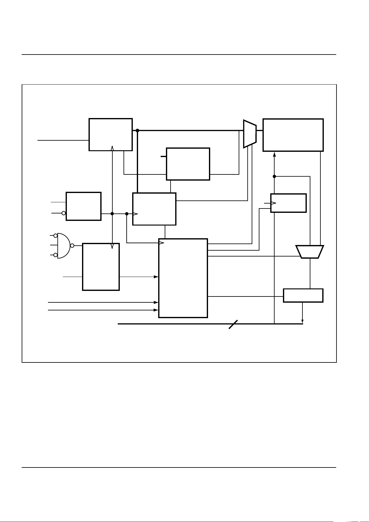
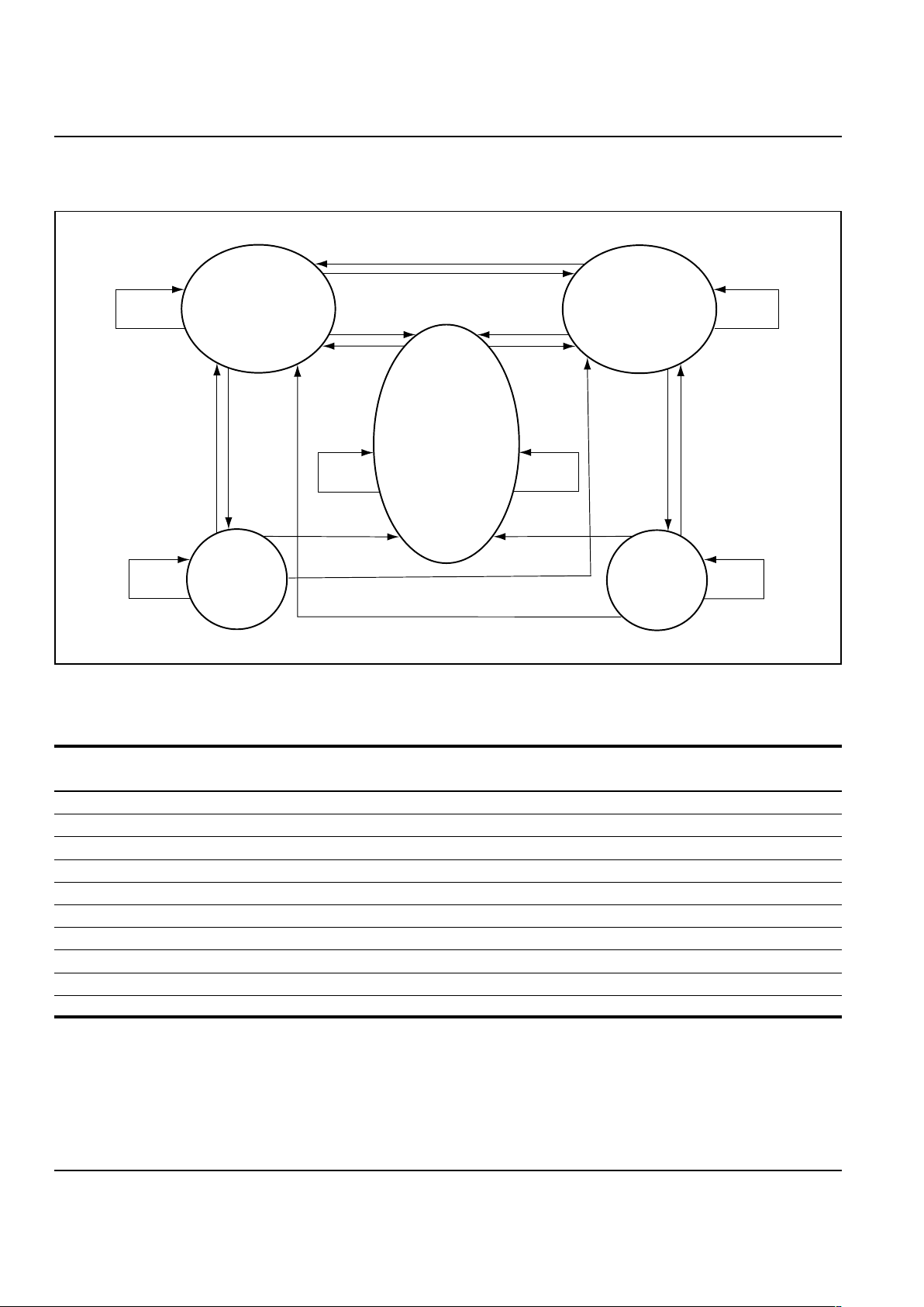
BLOCK DIAGRAM
ADV
WE
}
BW
Ÿ
X
(X=a,b,c,d or a,b)
CE
CE2
CE2
CONTROL
LOGIC
256Kx32; 256Kx36;
512Kx18
MEMORY ARRAY
WRITE
ADDRESS
REGISTER
CONTROL
LOGIC
BUFFER
ADDRESS
REGISTER
A [0:17] or
A [0:18]
CLK
CKE
A2-A17 or A2-A18
A0-A1 A'0-A'1
BURST
ADDRESS
COUNTER
MODE
DATA -I N
REGISTER
CONTROL
REGISTER
OE
ZZ
32, 36 or 18
K
DQa0-DQd7 or DQa0-DQb8
DQPa-DQPd
K
Integrated Silicon Solution, Inc. — 1-800-379-4774
3
PRELIMINARY INFORMATION Rev. 00D
04/26/01
IS61NF25632 IS61NF25636 IS61NF51218
IS61NLF25632 IS61NLF25636 IS61NLF51218 ISSI
®
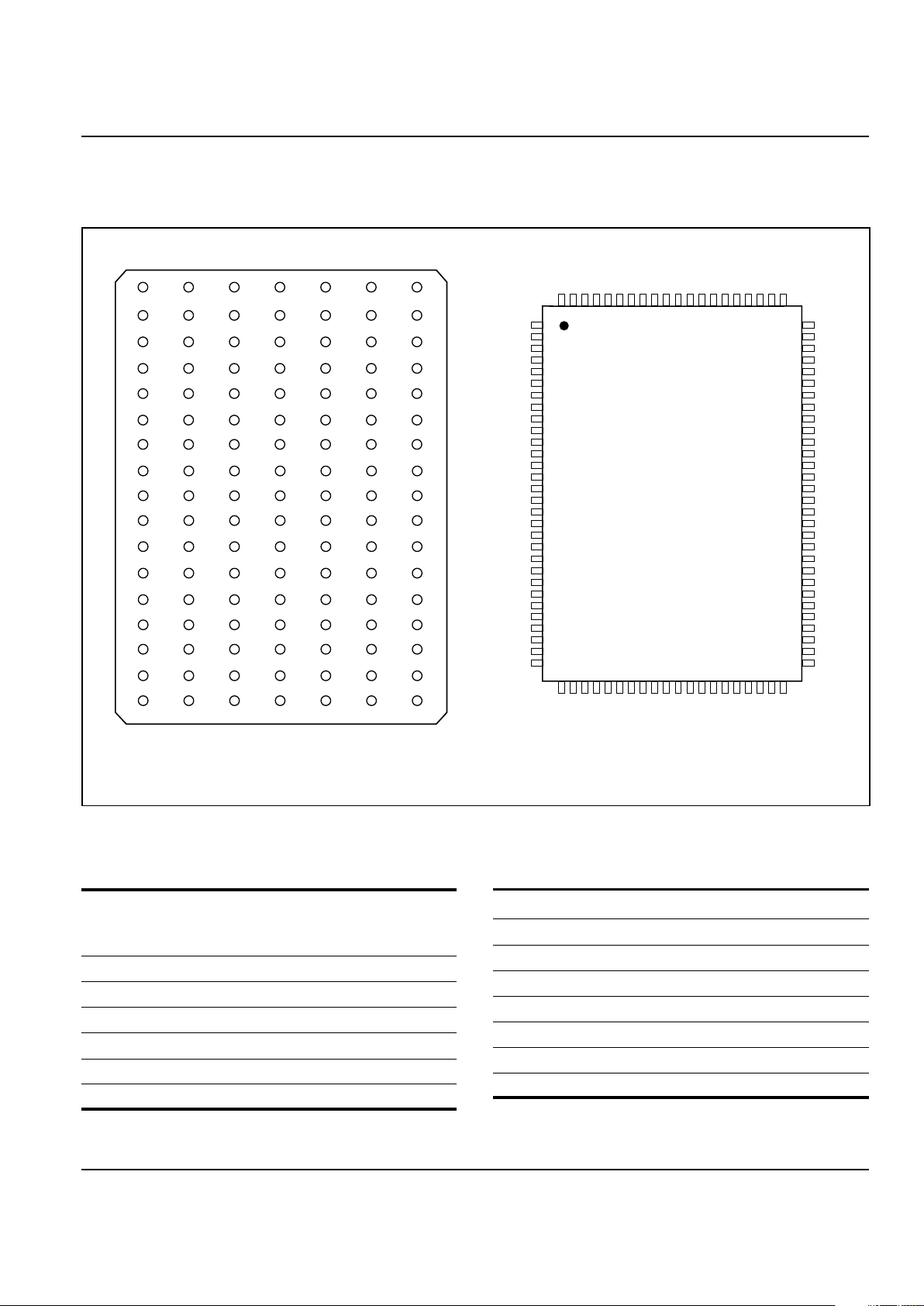
256K x 32
PIN DESCRIPTIONS
A0, A1 Synchronous Address Inputs. These
pins must tied to the two LSBs of the
address bus.
A2-A17 Synchronous Address Inputs
CLK Synchronous Clock
ADV Synchronous Burst Address Advance
BWa-BWd Synchronous Byte Write Enable
WE Write Enable
CKE Clock Enable
CE, CE2, CE2 Synchronous Chip Enable
OE Output Enable
DQa-DQd Synchronous Data Input/Output
MODE Burst Sequence Mode Selection
VCC +3.3V Power Supply
GND Ground
VCCQ
I
solated Output Buffer Supply: +3.3V/2.5V
ZZ Snooze Enable
PIN CONFIGURATION
119-pin PBGA (Top View) and 100-Pin TQFP
A
B
C
D
E
F
G
H
J
K
L
M
N
P
R
T
U
VCCQ
NC
NC
DQc1
DQc2
VCCQ
DQc5
DQc7
VCCQ
DQd1
DQd4
VCCQ
DQd6
DQd8
NC
NC
VCCQ
A6
CE2
A7
NC
DQc3
DQc4
DQc6
DQc8
VCC
DQd2
DQd3
DQd5
DQd7
NC
A5
NC
NC
A4
A3
A2
GND
GND
GND
BWc
GND
NC
GND
BWd
GND
GND
GND
MODE
A10
NC
NC
ADV
VCC
NC
CE
OE
A17
WE
VCC
CLK
NC
CKE
A1
A0
VCC
A11
NC
A8
A9
A12
GND
GND
GND
BWb
GND
NC
GND
BWa
GND
GND
GND
NC
A14
NC
A16
CE2
A15
NC
DQb6
DQb5
DQb4
DQb2
VCC
DQa7
DQa5
DQa4
DQa3
NC
A13
NC
NC
VCCQ
NC
NC
DQb8
DQb7
VCCQ
DQb3
DQb1
VCCQ
DQa8
DQa6
VCCQ
DQa2
DQa1
NC
ZZ
VCCQ
1 2 3 4 5 6 7
1
2
3
4
5
6
7
8
9
10
11
12
13
14
15
16
17
18
19
20
21
22
23
24
25
26
27
28
29
30
80
79
78
77
76
75
74
73
72
71
70
69
68
67
66
65
64
63
62
61
60
59
58
57
56
55
54
53
52
51
100
99 98 97 96 95 94 93 92 91 90 89 88 87 86 85 84 83 82 81
31 32 33 34 35 36 37 38 39 40 41 42 43 44 45 46 47 48 49 50
NC
DQc1
DQc2
VCCQ
GND
DQc3
DQc4
DQc5
DQc6
GND
VCCQ
DQc7
DQc8
GND
VCC
VCC
GND
DQd1
DQd2
VCCQ
GND
DQd3
DQd4
DQd5
DQd6
GND
VCCQ
DQd7
DQd8
NC
NC
DQb8
DQb7
VCCQ
GND
DQb6
DQb5
DQb4
DQb3
GND
VCCQ
DQb2
DQb1
GND
GND
VCC
ZZ
DQa8
DQa7
VCCQ
GND
DQa6
DQa5
DQa4
DQa3
GND
VCCQ
DQa2
DQa1
NC
MODE
A5A4A3A2A1
A0
NC
NC
GND
VCC
NC
NC
A10
A11
A12
A13
A14
A15
A16
A6A7CE
CE2
BWd
BWc
BWb
BWa
CE2
VCC
GND
CLKWECKEOEADVNCA17A8A9
4
Integrated Silicon Solution, Inc. — 1-800-379-4774
PRELIMINARY INFORMATION Rev. 00D
04/26/01
IS61NF25632 IS61NF25636 IS61NF51218
IS61NLF25632 IS61NLF25636 IS61NLF51218 ISSI
®
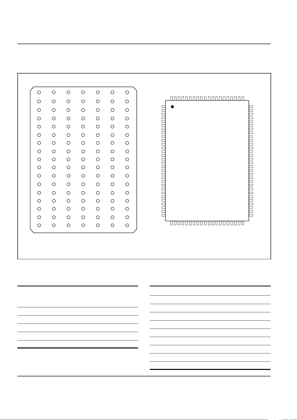
PIN CONFIGURATION
119-pin PBGA (Top View) and 100-Pin TQFP
PIN DESCRIPTIONS
A0, A1 Synchronous Address Inputs. These
pins must tied to the two LSBs of the
address bus.
A2-A17 Synchronous Address Inputs
CLK Synchronous Clock
ADV Synchronous Burst Address Advance
BWa-BWd Synchronous Byte Write Enable
WE Write Enable
CKE Clock Enable
CE, CE2, CE2 Synchronous Chip Enable
OE Output Enable
DQa-DQd Synchronous Data Input/Output
MODE Burst Sequence Mode Selection
VCC +3.3V Power Supply
GND Ground
VCCQ
solated Output Buffer Supply: +3.3V/2.5V
ZZ Snooze Enable
DQPa-DQPd Parity Data I/O
256K x 36
A
B
C
D
E
F
G
H
J
K
L
M
N
P
R
T
U
VCCQ
NC
NC
DQc1
DQc2
VCCQ
DQc5
DQc7
VCCQ
DQd1
DQd4
VCCQ
DQd6
DQd8
NC
NC
VCCQ
A6
CE2
A7
DQPc
DQc3
DQc4
DQc6
DQc8
VCC
DQd2
DQd3
DQd5
DQd7
DQPd
A5
NC
NC
A4
A3
A2
GND
GND
GND
BWc
GND
NC
GND
BWd
GND
GND
GND
MODE
A10
NC
NC
ADV
VCC
NC
CE
OE
A17
WE
VCC
CLK
NC
CKE
A1
A0
VCC
A11
NC
A8
A9
A12
GND
GND
GND
BWb
GND
NC
GND
BWa
GND
GND
GND
NC
A14
NC
A16
CE2
A15
DQPb
DQb6
DQb5
DQb4
DQb2
VCC
DQa7
DQa5
DQa4
DQa3
DQPa
A13
NC
NC
VCCQ
NC
NC
DQb8
DQb7
VCCQ
DQb3
DQb1
VCCQ
DQa8
DQa6
VCCQ
DQa2
DQa1
NC
ZZ
VCCQ
1 2 3 4 5 6 7
1
2
3
4
5
6
7
8
9
10
11
12
13
14
15
16
17
18
19
20
21
22
23
24
25
26
27
28
29
30
80
79
78
77
76
75
74
73
72
71
70
69
68
67
66
65
64
63
62
61
60
59
58
57
56
55
54
53
52
51
100
99 98 97 96 95 94 93 92 91 90 89 88 87 86 85 84 83 82 81
31 32 33 34 35 36 37 38 39 40 41 42 43 44 45 46 47 48 49 50
DQPc
DQc1
DQc2
VCCQ
GND
DQc3
DQc4
DQc5
DQc6
GND
VCCQ
DQc7
DQc8
GND
VCC
VCC
GND
DQd1
DQd2
VCCQ
GND
DQd3
DQd4
DQd5
DQd6
GND
VCCQ
DQd7
DQd8
DQPd
DQPb
DQb8
DQb7
VCCQ
GND
DQb6
DQb5
DQb4
DQb3
GND
VCCQ
DQb2
DQb1
GND
GND
VCC
ZZ
DQa8
DQa7
VCCQ
GND
DQa6
DQa5
DQa4
DQa3
GND
VCCQ
DQa2
DQa1
DQPa
MODE
A5A4A3A2A1
A0
NC
NC
GND
VCC
NC
NC
A10
A11
A12
A13
A14
A15
A16
A6A7CE
CE2
BWd
BWc
BWb
BWa
CE2
VCC
GND
CLKWECKEOEADVNCA17A8A9
Integrated Silicon Solution, Inc. — 1-800-379-4774
5
PRELIMINARY INFORMATION Rev. 00D
04/26/01
IS61NF25632 IS61NF25636 IS61NF51218
IS61NLF25632 IS61NLF25636 IS61NLF51218 ISSI
®
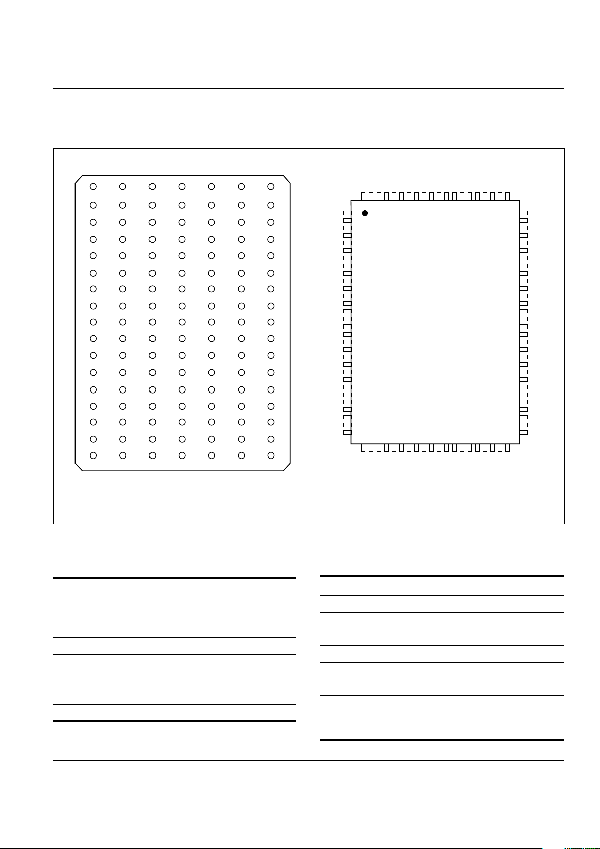
PIN CONFIGURATION
119-pin PBGA (Top View) and 100-Pin TQFP
PIN DESCRIPTIONS
A0, A1 Synchronous Address Inputs. These
pins must tied to the two LSBs of the
address bus.
A2-A18 Synchronous Address Inputs
CLK Synchronous Clock
ADV Synchronous Burst Address Advance
BWa-BWb Synchronous Byte Write Enable
WE Write Enable
CKE Clock Enable
CE, CE2, CE2 Synchronous Chip Enable
OE Output Enable
DQ1-DQ16 Synchronous Data Input/Output
MODE Burst Sequence Mode Selection
VCC +3.3V Power Supply
GND Ground
VCCQ
Isolated Output Buffer Supply: +3.3V/2.5V
ZZ Snooze Enable
DQP1-DQP2 Parity Data I/O DQP1 is parity for
DQ1-8; DQP2 is parity for DQ9-16
512K x 18
A
B
C
D
E
F
G
H
J
K
L
M
N
P
R
T
U
VCCQ
NC
NC
DQ9
NC
VCCQ
NC
DQ12
VCCQ
NC
DQ14
VCCQ
DQ16
NC
NC
NC
VCCQ
A6
CE2
A7
NC
DQ10
NC
DQ11
NC
VCC
DQ13
NC
DQ15
NC
DQP2
A5
A10
NC
A4
A3
A2
GND
GND
GND
BWb
GND
NC
GND
NC
GND
GND
GND
MODE
A11
NC
NC
ADV
VCC
NC
CE
OE
A17
WE
VCC
CLK
NC
CKE
A1
A0
VCC
NC
NC
A8
A9
A12
GND
GND
GND
NC
GND
NC
GND
BWa
GND
GND
GND
NC
A14
NC
A16
CE2
A15
DQP1
NC
DQ7
NC
DQ5
VCC
NC
DQ3
NC
DQ2
NC
A13
A18
NC
VCCQ
NC
NC
NC
DQ8
VCCQ
DQ6
NC
VCCQ
DQ4
NC
VCCQ
NC
DQ1
NC
ZZ
VCCQ
1 2 3 4 5 6 7
1
2
3
4
5
6
7
8
9
10
11
12
13
14
15
16
17
18
19
20
21
22
23
24
25
26
27
28
29
30
80
79
78
77
76
75
74
73
72
71
70
69
68
67
66
65
64
63
62
61
60
59
58
57
56
55
54
53
52
51
100
99 98 97 96 95 94 93 92 91 90 89 88 87 86 85 84 83 82 81
31 32 33 34 35 36 37 38 39 40 41 42 43 44 45 46 47 48 49 50
NC
NC
NC
VCCQ
GND
NC
NC
DQ9
DQ10
GND
VCCQ
DQ11
DQ12
GND
VCC
VCC
GND
DQ13
DQ14
VCCQ
GND
DQ15
DQ16
DQP2
NC
GND
VCCQ
NC
NC
NC
A10
NC
NC
VCCQ
GND
NC
DQP1
DQ8
DQ7
GND
VCCQ
DQ6
DQ5
GND
GND
VCC
ZZ
DQ4
DQ3
VCCQ
GND
DQ2
DQ1
NC
NC
GND
VCCQ
NC
NC
NC
MODE
A5A4A3A2A1
A0
NC
NC
GND
VCC
NC
NC
A11
A12
A13
A14
A15
A16
A17
A6A7CE
CE2NCNC
BWb
BWa
CE2
VCC
GND
CLKWECKEOEADVNCA18A8A9
6
Integrated Silicon Solution, Inc. — 1-800-379-4774
PRELIMINARY INFORMATION Rev. 00D
04/26/01
IS61NF25632 IS61NF25636 IS61NF51218
IS61NLF25632 IS61NLF25636 IS61NLF51218 ISSI
®
SYNCHRONOUS TRUTH TABLE
(1)
Address
Operation Used CS1 CS2 CS2 ADV WE BWx OE CKE CLK
Not Selected Continue N/A X X X H X X X L ↑
Begin Burst Read External Address L H L L H X L L ↑
Continue Burst Read Next Address X X X H X X L L ↑
NOP/Dummy Read External Address L H L L H X H L ↑
Dummy Read Next Address X X X H X X H L ↑
Begin Burst Write External Address L H L L L L X L ↑
Continue Burst Write Next Address X X X H X L X L ↑
NOP/Write Abort N/A L H L L L H X L ↑
Write Abort Next Address X X X H X H X L ↑
Ignore Clock Current Address X X X X X X X H ↑
Notes:
1. "X" means don't care.
2. The rising edge of clock is symbolized by ↑
3. A continue deselect cycle can only be entered if a deselect cycle is executed first.
4. WE = L means Write operation in Write Truth Table.
WE = H means Read operation in Write Truth Table.
5. Operation finally depends on status of asynchronous pins (ZZ and OE).
BURST
READ
DESELECT
BURST
WRITE
BEGIN
READ
BEGIN
WRITE
READ
WRITE
READ
WRITE
BURST
BURST
BURST
DS
DS
DS
READ
DSDS
READ WRITE
WRITE
BURST
BURST
WRITE
READ
STATE DIAGRAM
 Loading...