


IS41LV8200-50JI
ISSI IS41LV8200-50JI, IS41LV8200-50J, IS41C8200-50JI, IS41C8200-50J, IS41C8200-60JI Datasheet
...
IS41C8200
IS41LV8200 ISSI
2M x 8 (16-MBIT) DYNAMIC RAM
®
WITH EDO PAGE MODE
FEATURES
• Extended Data-Out (EDO) Page Mode access cycle
• TTL compatible inputs and outputs
• Refresh Interval:
-- 2,048 cycles/32 ms
• Refresh Mode: RAS-Only,
CAS-before-RAS (CBR), and Hidden
• Single power supply:
5V±10% or 3.3V ± 10%
• Byte Write and Byte Read operation via two CAS
• Industrial temperature range -40°C to 85°C
PRODUCT SERIES OVERVIEW
Part No. Refresh Voltage
IS41C8200 2K 5V ± 10%
IS41LV8200 2K 3.3V ± 10%
JUNE 2001
DESCRIPTION
The
ISSI
IS41C8200 and IS41LV8200 are 2,097,152 x 8-bit
highperformance CMOS Dynamic Random Access Memory.
These devices offer an accelarated cycle access called
EDO Page Mode. EDO Page Mode allows 2,048 random
accesses within a single row with access cycle time as
short as 20 ns per 4-bit word.
These features make the IS41C8200 and IS41LV8200
ideally suited for high-bandwidth graphics, digital signal
processing, high-performance computing systems, and
peripheral applications.
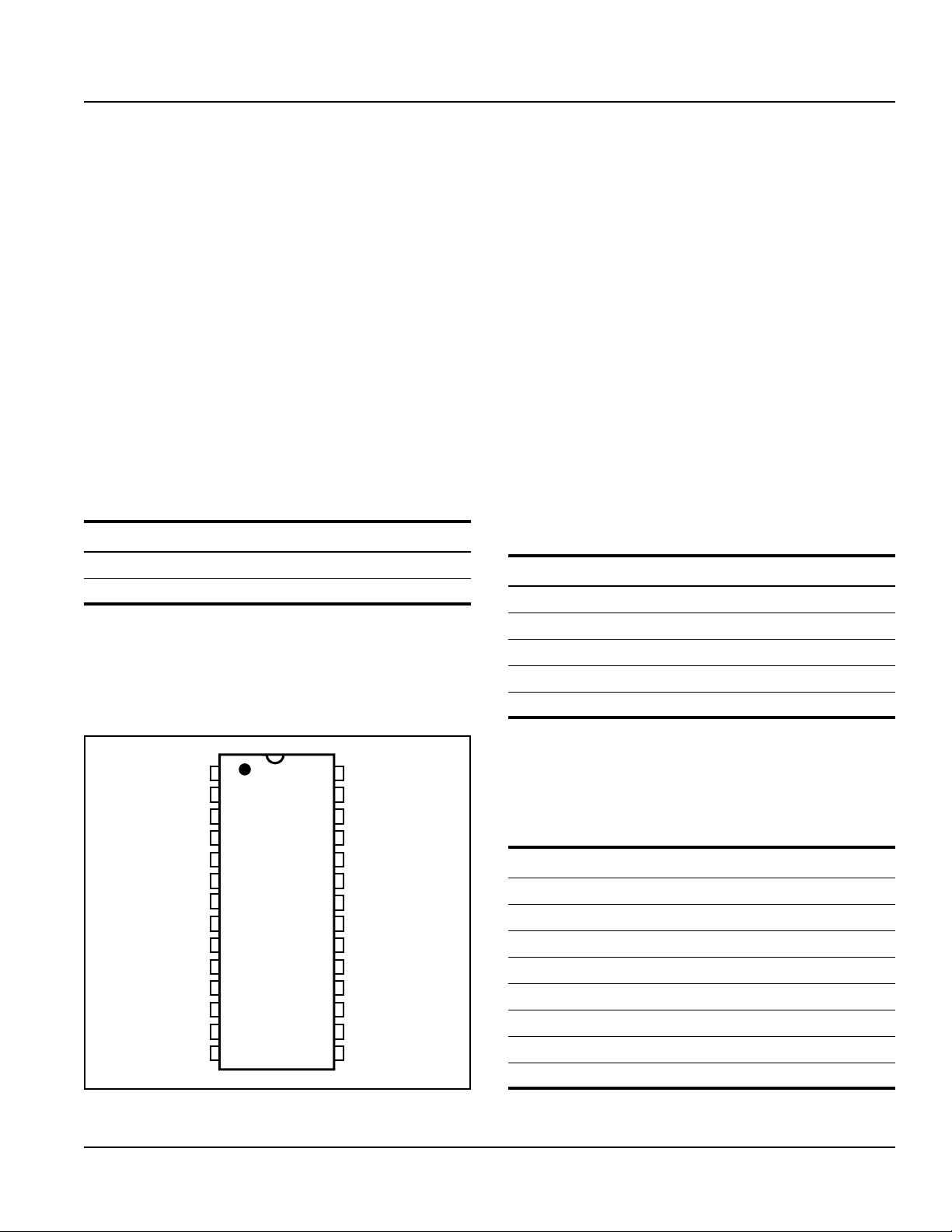
The IS41C8200 and IS41LV8200 are packaged in 28-pin
300-mil SOJ with JEDEC standard pinouts.
KEY TIMING PARAMETERS
Parameter -50 -60 Unit
RAS Access Time (tRAC)5060ns
CAS Access Time (tCAC)1315ns
PIN CONFIGURATION
28 Pin SOJ
NC
A0
A1
A2
A3
1
2
3
4
5
6
7
8
9
10
11
12
13
14
VCC
I/O0
I/O1
I/O2
I/O3
WE
RAS
A10
VCC
28
27
26
25
24
23
22
21
20
19
18
17
16
15
GND
I/O7
I/O6
I/O5
I/O4
CAS
OE
A9
A8
A7
A6
A5
A4
GND
Column Address Access Time (tAA)
EDO Page Mode Cycle Time (tPC)
25 30 ns
20 25 ns
Read/Write Cycle Time (tRC) 84 104 ns
PIN DESCRIPTIONS
A0-A10 Address Inputs
I/O0-7 Data Inputs/Outputs
WE Write Enable
OE Output Enable
RAS Row Address Strobe
CAS Column Address Strobe
Vcc Power
GND Ground
NC No Connection
ISSI reserves the right to make changes to its products at any time without notice in order to improve design and supply the best possible product. We assume no responsibility for any
errors which may appear in this publication. © Copyright 2001, Integrated Silicon Solution, Inc.
Integrated Silicon Solution, Inc. — 1-800-379-4774
Rev. B
06/22/01
1
IS41C8200
IS41LV8200 ISSI
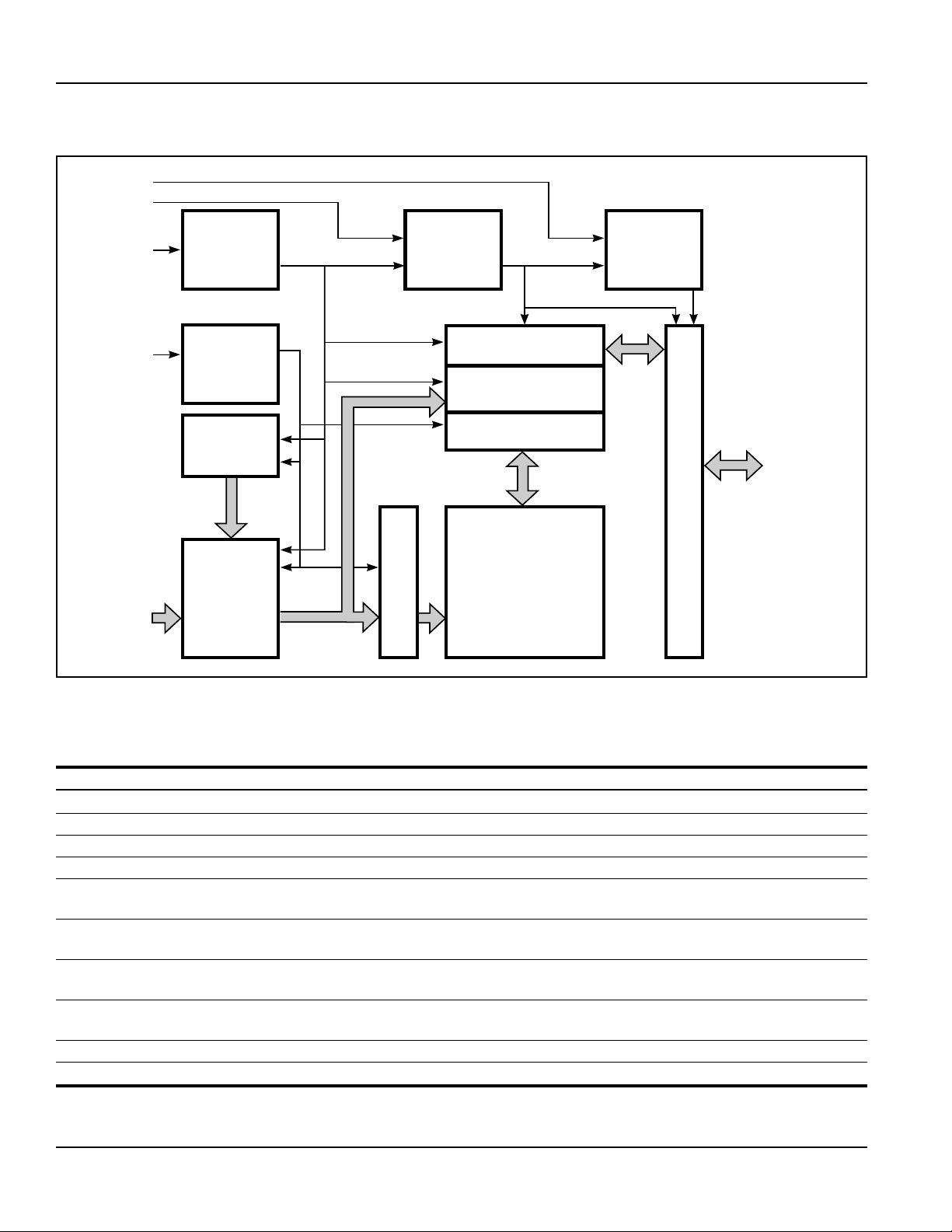
FUNCTIONAL BLOCK DIAGRAM
OE
WE
®
CAS
RAS
A0-A10
CAS
CONTROL
LOGIC
RAS
CLOCK
GENERATOR
REFRESH
COUNTER
ADDRESS
BUFFERS
WE
CAS WE
RAS
CONTROL
LOGIC
COLUMN DECODER
SENSE AMPLIFIERS
ROW DECODER
OE
CONTROL
LOGIC
OE
DATA I/O BUS
I/O0-I/O7
DATA I/O BUFFERS
MEMORY ARRAY
2,097,152 x 8
TRUTH TABLE
Function RAS CAS WE OE Address tR/tC I/O
Standby H H X X X High-Z
Read L L H L ROW/COL DOUT
Write: Word (Early Write) L L L X ROW/COL DIN
Read-Write L L H→LL→H ROW/COL DOUT, DIN
EDO Page-Mode Read 1st Cycle: L H→L H L ROW/COL DOUT
2nd Cycle: L H→L H L NA/COL DOUT
EDO Page-Mode Write 1st Cycle: L H→ L L X ROW/COL DIN
2nd Cycle: L H→L L X NA/COL DIN
EDO Page-Mode 1st Cycle: L H→LH→LL→H ROW/COL DOUT, DIN
Read-Write 2nd Cycle: L H→LH→LL→H NA/COL DOUT, DIN
Hidden Refresh Read L→H→L L H L ROW/COL DOUT
RAS-Only Refresh L H X X ROW/NA High-Z
CBR Refresh H→L L X X X High-Z
Note:
1. EARLY WRITE only.
2
Write
(1)
L→H→L L L X ROW/COL DOUT
Integrated Silicon Solution, Inc. — 1-800-379-4774
Rev. B
06/22/01

IS41C8200
IS41LV8200 ISSI
®
Functional Description
The IS41C8200 and IS41LV8200 are CMOS DRAMs
optimized for
During READ or WRITE cycles, each bit is uniquely
addressed through the 11 address bits. These are entered
11 bits (A0-A10) at a time. The row address is latched by
the Row Address Strobe (RAS). The column address is
latched by the Column Address Strobe (CAS). RAS is
used to latch the first nine bits and CAS is used the latter
ten bits.
high-speed bandwidth, low power applications.
Memory Cycle
A memory cycle is initiated by bring RAS LOW and it is
terminated by returning both RAS and CAS HIGH. To
ensures proper device operation and data integrity any
memory cycle, once initiated, must not be ended or
aborted before the minimum tRAS time has expired. A new
cycle must not be initiated until the minimum precharge
time tRP, tCP has elapsed.
Read Cycle
A read cycle is initiated by the falling edge of CAS or OE,
whichever occurs last, while holding WE HIGH. The
column address must be held for a minimum time specified
by tAR. Data Out becomes valid only when tRAC, tAA, tCAC
and tOEA are all satisfied. As a result, the access time is
dependent on the timing relationships between these
parameters.
Auto Refresh Cycle
To retain data, 2,048 refresh cycles are required in each
32 ms period. There are two ways to refresh the memory:
1. By clocking each of the 2,048 row addresses (A0
through A10) with RAS at least once every 32 ms. Any
read, write,
the addressed row.
2. Using a
refresh is activated by the falling edge of RAS, while
holding CAS LOW. In CAS-before-RAS refresh cycle,
an internal 9-bit counter provides the row addresses
and the external address inputs are ignored.
CAS-before-RAS is a refresh-only mode and no data
access or device selection is allowed. Thus, the output
remains in the High-Z state during the cycle.
read-modify-write
CAS-before-RAS
or
RAS-only
refresh cycle.
cycle refreshes
CAS-before-RAS
Power-On
After application of the VCC supply, an initial pause of
200 µs is required followed by a minimum of eight
initialization cycles (any combination of cycles containing a RAS signal).
During power-on, it is recommended that RAS track with
VCC or be held at a valid VIH to avoid current surges.
Write Cycle
A write cycle is initiated by the falling edge of CAS and
WE, whichever occurs last. The input data must be valid
at or before the falling edge of CAS or WE, whichever
occurs last.
Integrated Silicon Solution, Inc. — 1-800-379-4774
Rev. B
06/22/01
3

IS41C8200
IS41LV8200 ISSI
®
ABSOLUTE MAXIMUM RATINGS
(1)
Symbol Parameters Rating Unit
VT Voltage on Any Pin Relative to GND 5V –1.0 to +7.0 V
3.3V –0.5 to +4.6
CC Supply Voltage 5V –1.0 to +7.0 V
V
3.3V –0.5 to +4.6
IOUT Output Current 50 mA
PD Power Dissipation 1 W
A Commercial Operation Temperature 0 to +70 °C
T
Industrial Operation Temperature -40 to +85
TSTG Storage Temperature –55 to +125 °C
Note:
1. Stress greater than those listed under ABSOLUTE MAXIMUM RATINGS may cause permanent damage to the device.
This is a stress rating only and functional operation of the device at these or any other conditions above those indicated
in the operational sections of this specification is not implied. Exposure to absolute maximum rating conditions for extended
periods may affect reliability.
RECOMMENDED OPERATING CONDITIONS (Voltages are referenced to GND.)
Symbol Parameter Min. Typ. Max. Unit
VCC Supply Voltage 5V 4.5 5.0 5.5 V
3.3V 3.0 3.3 3.6
VIH Input High Voltage 5V 2.4 — VCC + 1.0 V
3.3V 2.0 — VCC + 0.3
VIL Input Low Voltage 5V –1.0 — 0.8 V
3.3V –0.3 — 0.8
TA Commercial Ambient Temperature 0 — 70 °C
Industrial Ambient Temperature -40 — 85 °C
CAPACITANCE
Symbol Parameter Max. Unit
CIN1 Input Capacitance: A0-A10(A11) 5 pF
CIN2 Input Capacitance: RAS, CAS, WE, OE 7pF
CIO Data Input/Output Capacitance: I/O0-I/O3 7 pF
Notes:
1. Tested initially and after any design or process changes that may affect these parameters.
2. Test conditions: T
(1,2)
A = 25°C, f = 1 MHz.
4
Integrated Silicon Solution, Inc. — 1-800-379-4774
Rev. B
06/22/01

IS41C8200
IS41LV8200 ISSI
®
ELECTRICAL CHARACTERISTICS
(1)
(Recommended Operating Conditions unless otherwise noted.)
Symbol Parameter Test Condition VCC Speed Min. Max. Unit
IIL Input Leakage Current Any input 0V ≤ VIN ≤ Vcc –55µA
Other inputs not under test = 0V
IIO Output Leakage Current Output is disabled (Hi-Z) –55µA
0V ≤ VOUT ≤ Vcc
OH
V
Output High Voltage Level
IOH = –5.0 mA, Vcc = 5V 2.4 — V
IOH = –2.0 mA, Vcc = 3.3V
V
OL
Output Low Voltage Level
IOL = 4.2 mA, Vcc = 5V — 0.4 V
IOL = 2 mA, Vcc = 3.3V
ICC1 Standby Current: TTL RAS, CAS ≥ VIH
Commercial
5V 2 mA
3.3V — 0.5
Industrial
5V — 3
3.3V — 2
ICC2 Standby Current: CMOS RAS, CAS ≥ VCC – 0.2V 5V — 1mA
3.3V — 0.5
ICC3 Operating Current: RAS, CAS, -50 — 120 mA
Random Read/Write
(2,3,4)
Address Cycling, tRC = tRC (min.)
-60 — 110
Average Power Supply Current
ICC4 Operating Current: RAS= VIL, CAS ≥ VIH -50 — 90 mA
EDO Page Mode
(2,3,4)
tRC = tRC (min.) -60 — 80
Average Power Supply Current
ICC5 Refresh Current: RAS Cycling, CAS ≥ VIH -50 — 120 mA
RAS-Only
(2,3)
tRC = tRC (min.) -60 — 110
Average Power Supply Current
ICC6 Refresh Current: RAS, CAS Cycling -50 — 120 mA
(2,3,5)
CBR
tRC = tRC (min.) -60 — 110
Average Power Supply Current
Notes:
1. An initial pause of 200 µs is required after power-up followed by eight RAS refresh cycles (RAS-Only or CBR) before proper device
operation is assured. The eight RAS cycles wake-up should be repeated any time the t
2. Dependent on cycle rates.
3. Specified values are obtained with minimum cycle time and the output open.
4. Column-address is changed once each EDO Page cycle.
5. Enables on-chip refresh and address counters.
REF refresh requirement is exceeded.
Integrated Silicon Solution, Inc. — 1-800-379-4774
Rev. B
06/22/01
5

IS41C8200
IS41LV8200 ISSI
®
AC CHARACTERISTICS
(1,2,3,4,5,6)
(Recommended Operating Conditions unless otherwise noted.)
-50 -60
Symbol Parameter Min. Max. Min. Max. Units
tRC Random READ or WRITE Cycle Time 84 — 104 — ns
tRAC Access Time from RAS
tCAC Access Time from CAS
tAA Access Time from Column-Address
(6, 7)
(6, 8, 15)
— 50 — 60 ns
— 13 — 15 ns
(6)
— 25 — 30 ns
tRAS RAS Pulse Width 50 10K 60 10K ns
tRP RAS Precharge Time 30 — 40 — ns
(21)
(23)
8 10K 10 10K ns
(9)
9 — 9 — ns
38 — 40 — ns
(10, 20)
12 37 14 45 ns
tCAS CAS Pulse Width
tCP CAS Precharge Time
tCSH CAS Hold Time
tRCD RAS to CAS Delay Time
tASR Row-Address Setup Time 0 — 0 — ns
tRAH Row-Address Hold Time 8 — 10 — ns
(20)
(20)
0 — 0 — ns
8 — 10 — ns
tASC Column-Address Setup Time
tCAH Column-Address Hold Time
tAR Column-Address Hold Time 30 — 40 — ns
(referenced to RAS)
tRAD RAS to Column-Address Delay Time
(11)
10 25 12 30 ns
tRAL Column-Address to RAS Lead Time 25 — 30 — ns
tRPC RAS to CAS Precharge Time 5 — 5 — ns
tRSH RAS Hold Time 8 — 10 — ns
tRHCP RAS Hold Time from CAS Precharge 30 — 35 — ns
(19, 24)
(15, 16)
(15, 24)
(21)
0 — 0 — ns
5 — 5 — ns
315 315 ns
— 12 — 15 ns
tCLZ CAS to Output in Low-Z
tCRP CAS to RAS Precharge Time
tOD Output Disable Time
tOE Output Enable Time
tOED Output Enable Data Delay (Write) 12 — 15 — ns
tOEHC OE HIGH Hold Time from CAS HIGH 5 — 5 — ns
tOEP OE HIGH Pulse Width 10 — 10 — ns
tOES OE LOW to CAS HIGH Setup Time 5 — 5 — ns
tRCS Read Command Setup Time
(17, 20)
0 — 0 — ns
tRRH Read Command Hold Time 0 — 0 — ns
(referenced to RAS)
(12)
tRCH Read Command Hold Time 0 — 0 — ns
(referenced to CAS)
tWCH Write Command Hold Time
(12, 17, 21)
(17)
8 — 10 — ns
tWCR Write Command Hold Time 40 — 50 — ns
(referenced to RAS)
tWP Write Command Pulse Width
(17)
(17)
8 — 10 — ns
tWPZ WE Pulse Widths to Disable Outputs 7 — 7 — ns
6
Integrated Silicon Solution, Inc. — 1-800-379-4774
Rev. B
06/22/01
 Loading...