


IS41LV32256-35TQ
ISSI IS41LV32256-35TQ, IS41LV32256-35PQ, IS41LV32256-30TQ, IS41LV32256-30PQ, IS41LV32256-28TQ Datasheet
...
IS41LV32256 ISSI
256K x 32 (8-Mbit) EDO DYNAMIC RAM
SEPTEMBER 2000
3.3V, 100/83/66 MHz
®
FEATURES
• 262,144-word by 32-bit organization
• Single +3.3V ± 0.3V power supply
• Four CAS inputs for Byte Write and Byte Read
control
• Refresh modes: RAS-Only, CAS-Before-RAS (CBR),
and Hidden
• 512-cycle refresh in 8 ms
• Fast Page Mode with Extended Data Out
• 100-pin PQFP, TQFP package
DESCRIPTION
The ISSI IS41LV32256 is organized in a 262,122 x 32-bit
CMOS Dynamic Random Access Memory. Four CAS signals
facilitate execution of Byte Read and Byte Write operations.
A very fast EDO cycle time of 10 ns allows an operating
frequency of 100 MHz and makes the IS41LV32256 an ideal
frame buffer memory for graphics applications.
The IS41LV32256 is compatible with JEDEC standard
SGRAMs. This 8-Mbit EDO memory offers a significantly
lower latency and a faster memory cycle than the SGRAM.
ISSI's IS41LV32256 3.3V 256K x 32 device is pin/voltage
compatible with all standard SGRAM parts.
The IS41LV32256 is available in a 100-pin PQFP and TQFP
package.
KEY TIMING PARAMETERS
Parameter -28 -30 -35 Unit
Max. RAS Access Time (tRAC) 283035ns
Max. CAS Access Time (tCAC)9910ns
Max. Column Address Access Time (tAA)151618ns
Max. OE Access Time (tOE)9910ns
Min. Read/Write Cycle Time (tRC) 485360ns
Min. EDO Cycle Time (tPC) 121215ns
ISSI reserves the right to make changes to its products at any time without notice in order to improve design and supply the best possible product. We assume no responsibility for any errors
which may appear in this publication. © Copyright 2000, Integrated Silicon Solution, Inc.
Integrated Silicon Solution, Inc.
Rev. A
09/29/00
1
IS41LV32256 ISSI
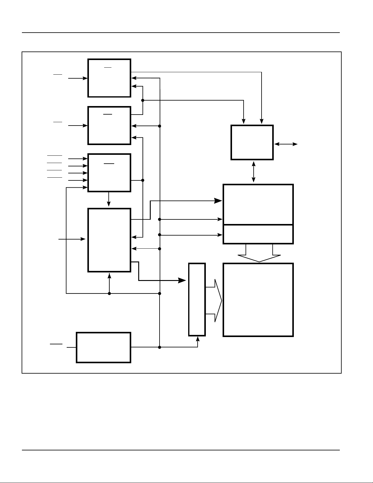
FUNCTIONAL BLOCK DIAGRAM
OE
OE
WE
CAS0
CAS1
CAS2
CAS3
CLOCK
GENERATOR
WE
CLOCK
GENERATOR
CAS
CLOCK
GENERATOR
Data I/O
Buffers
I/O0-31
®
A0-A8
RAS
CONTROLS
RAS
CLOCK
GENERATOR
AX0-AX8
AY0-AY8
512
ROW DECODERS
COLUMN DECODERS
SENSE AMPLIFIERS
512 x 32
MEMORY ARRAY
256K x 32
2
Integrated Silicon Solution, Inc.
Rev. A
09/29/00
IS41LV32256 ISSI
3
1
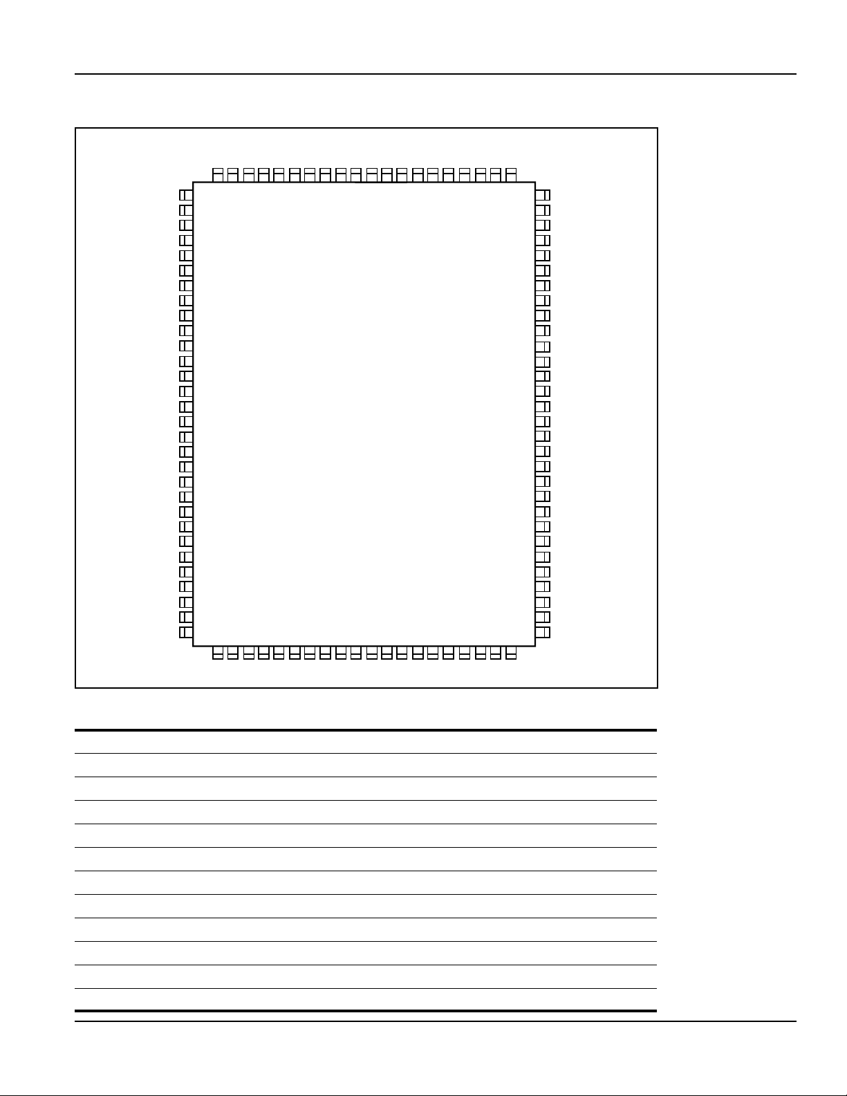
PIN CONFIGURATIONS
100-Pin PQFP, TQFP
I/O2
GND
I/O1
I/O0
VccNCNCNCNCNCNCNCNCNCNC
GND
I/O31
I/O30
GND
I/O29
®
I/O3
Vcc
I/O4
I/O5
GND
I/O6
I/O7
Vcc
I/O16
I/O17
GND
I/O18
I/O19
Vcc
Vcc
GND
I/O20
I/O21
GND
I/O22
I/O23
Vcc
CAS0
CAS2
WE
NC
NC
RAS
NC
NC
99989796959493929190898887868584838281
1
100
2
3
4
5
6
7
8
9
10
11
12
13
14
15
16
17
18
19
20
21
22
23
24
25
26
27
28
29
30
31323334353637383940414243444546474849
50
80
I/O28
79
Vcc
78
I/O27
77
I/O26
76
GND
75
I/O25
74
I/O24
73
Vcc
72
I/O15
71
I/O14
70
GND
69
I/O13
68
I/O12
67
Vcc
66
GND
65
Vcc
64
I/O11
63
I/O10
62
GND
61
I/O9
60
I/O8
59
Vcc
58
NC
57
CAS
56
CAS
55
NC
54
NC
53
OE
52
NC
51
A8
A0A1A2
A3
PIN DESCRIPTIONS
A0-A8 Address Inputs
RAS Row Address Strobe
CAS0 Column Address Strobe for First Byte (I/O0-I/O7)
CAS1 Column Address Strobe for Second Byte (I/O8-I/O15)
CAS2 Column Address Strobe for Third Byte (I/O16-I/O23)
CAS3 Column Address Strobe for Fourth Byte (I/O24-I/O31)
WE Write Enable
OE Output Enable
I/O0-I/O31 Data Inputs/Outputs
Vcc +3.3V Supply
GND Ground
NC No Connection: This pin should be left unconnected or tied to ground.
Integrated Silicon Solution, Inc.
Rev. A
09/29/00
NCNCNCNCNCNCNCNCNC
Vcc
A4A5A6
NC
GND
A7
3

IS41LV32256 ISSI
TRUTH TABLE
Function RA S CAS0 CAS1 CAS2 CAS3 WE OE Address I/O
Standby H HHHHXX X High-Z
Read: Double Word L LLLLHLROW/COL DOUT
Read: 1st Byte L L H H H H L ROW/COL I/O0-7=DOUT;
I/O8-31=High-Z
Read: 2nd Byte L H L H H H L ROW/COL I/O0-7=High-Z;
I/O8-15=DOUT;
I/O16-31=High-Z
Read: 3rd Byte L H H L H H L ROW/COL I/O0-15=High-Z;
I/O16-23=DOUT;
I/O24-31=High-Z
Read: 4th Byte L H H H L H L ROW/COL I/O0-23=High-Z;
I/O24-31=DOUT
Write: Double Word (Early) L LLLLLXROW/COL DIN
Write: 1st Byte (Early) L L H H H L X ROW/COL I/O0-7=DIN;
I/O8-31=X
Write: 2nd Byte (Early) L H L H H L X ROW/COL I/O0-8=X;
I/O8-15=DIN;
I/O16-31=X
Write: 3rd Byte (Early) L H H L H L X ROW/COL I/O0-15=X;
I/O16-23=DIN;
I/O24-31=X
Write: 4th Byte (Early) L H H H L L X ROW/COL I/O0-23=X;
I/O24-31=DIN
Read-Write
Fast-Page-Mode Read: EDO
Fast-Page-Mode Read: High-Z
Fast-Page-Mode Write: (Early)
Fast-Page-Mode Read-Write
Hidden Refresh Read
Hidden Refresh Write
RAS-Only Refresh LHHHHXX ROW High-Z
CBR Refresh
Notes:
1. BYTE WRITE may be executed with CAS0, CAS1, CAS2 or CAS3 active.
2. BYTE READ may be executed with CAS0, CAS1, CAS2 or CAS3 active.
3. Only one CAS signal (CAS0, CAS1, CAS2 or CAS3) must be active.
(1,2)
LLLLLH∅LL∅H ROW/COL DOUT∅DIN
(2)
1st Cycle: L H∅LH∅LH∅LH∅L H L ROW/COL DOUT
Subsequent Cycles: L H∅LH∅LH∅LH∅L H L COL DOUT
(2)
1st Cycle: L H∅LH∅LH∅LH∅LHH∅L ROW/COL DOUT
Subsequent Cycles: L H∅LH∅LH∅LH∅LHH∅L COL DOUT
(1)
1st Cycle: L H∅LH∅LH∅LH∅L L X ROW/COL DIN
Subsequent Cycles: L H∅LH∅LH∅LH∅L L X COL DIN
(1,2
)
1st Cycle: L H∅LH∅LH∅LH∅LH∅LL∅ H ROW/COL DOUT∅DIN
Subsequent Cycles: L H∅LH∅LH∅LH∅LH∅LL∅ H COL DOUT∅DIN
(2)
(1)
(3)
L∅H∅LLLLLHLROW/COL DOUT
L∅H∅LLLLLLXROW/COLDIN∅High-Z
H∅LLLLLXX X High-Z
®
4
Integrated Silicon Solution, Inc.
Rev. A
09/29/00

IS41LV32256 ISSI
POWER-ON
The initial application of the VCC supply requires a 200-µs
wait followed by a minimum of any eight initialization
cycles containing a RAS clock. During Power-On, the VCC
current is dependent on the input levels of RAS and CAS.
It is recommended that RAS and CAS track with VCC or be
held at a valid VIH during Power-On to avoid current
surges.
®
ABSOLUTE MAXIMUM RATINGS
(1)
Symbol Parameters Rating Unit
tA Ambient Temperature Under Bias –1.0 to +80 °C
tSTG Storage Temperature –50 to +125 °C
VT Voltage Relative to GND –1.0 to +5.5 V
IOUT Data Output Current 50 mA
PD Power Dissipation 1.0 W
Note:
1. Stress greater than those listed under ABSOLUTE MAXIMUM RATINGS may cause permanent
damage to the device. This is a stress rating only and functional operation of the device at these
or any other conditions above those indicated in the operational sections of this specification is
not implied. Exposure to absolute maximum rating conditions for extended periods may affect
reliability.
RECOMMENDED OPERATING CONDITIONS
(1)
(TA = 0°C to 70°C)
Symbol Parameter Min. Typ. Max. Unit
VCC Power Supply 3.0 3.3 3.6 V
VIH Input High Voltage 2.4 — VCC + 0.5 V
VIL Input Low Voltage –0.5 — 0.4 V
Note:
1. Voltages are referenced to GND.
CAPACITANCE
(1,2)
Symbol Parameter Max. Unit
CIN Input Capacitance 5 pF
CIO Data Input/Output Capacitance 7 pF
Notes:
1. Capacitance is sampled and 100% tested.
2. Test conditions: TA = 25°C, f = 1 MHz, VCC = 3.3V.
Integrated Silicon Solution, Inc.
Rev. A
09/29/00
5

IS41LV32256 ISSI
DC CHARACTERISTICS (TA = 0°C to 70°C, VCC = 3.3V ± 0.3V)
-28 -30 -35
Symbol Parameter Condition Min. Max. Min. Max. Min. Max. Units
VIH Input HIGH (Logic 1) Voltage, All Inputs — 2.0 Vcc + 0.5 2.0 Vcc + 0.5 2.0 Vcc + 0.5 V
VIL Input LOW (Logic 1) Voltage, All Inputs —–0.5 0.8 –0.5 0.8 –0.5 0.8 V
VOH Output HIGH Voltage IOH = –2 mA 2.4 Vcc 2.4 Vcc 2.4 Vcc V
VOL Output LOW Voltage IOL = 2 mA 00.4 00.4 00.4 V
ILI Input Leakage Current 0V < VIN < VCC –10 10 –10 10 –10 10 µA
I
LO Output Leakage Current 0V < VOUT < 3.6V; –10 10 –10 10 –10 10 µA
Output Disable
ICC1 Average Power Supply Current RAS, CAS Cycling; — 250 — 250 — 240 mA
(Operating)
ICC2 Power Supply Current (Standby) RAS, CAS = VIH — 2.5 — 2.5 — 2.5 mA
Icc3 Average Power Supply Current RAS = Cycling; — 250 — 250 — 240 mA
(RAS-Only Refresh)
ICC4 Average Power Supply Current RAS = VIL; — 230 — 230 — 220 mA
(Fast Page Mode)
ICC5 Average Power Supply Current RAS = Cycling; — 250 — 250 — 240 mA
(CAS-before-RAS Refresh)
ICC6 CMOS Standby Current RAS, CAS = VCC –0.2V — 600 — 600 — 600 µA
(2,3,15,16)
(2,3,15,16)
(2,3,15,18)
(2,3,15.16)
tRC = Min.
CAS = VIH; tRC = Min.
CAS = Cycling; tPC = Min.
CAS-before-RAS
®
AC CHARACTERISTICS
(1,2,3,4,5,6)
(Recommended Operating Conditions unless otherwise noted.)
-28 -30 -35
Symbol Parameter Min. Max. Min. Max. Min. Max. Units
tRC Random READ or WRITE Cycle Time 48 — 53 — 60 — ns
tRAC Access Time from RAS
tCAC Access Time from CAS
tAA Access Time from Column-Address
(6, 7)
(6, 8, 15)
— 28 — 30 — 35 ns
— 9 — 9 — 10 ns
(6)
— 15 — 16 — 18 ns
tRAS RAS Pulse Width 28 10K 30 10K 35 10K ns
tRP RAS Precharge Time 17 — 18 — 20 — ns
(21)
(26)
(9, 25)
(10, 20)
5 10K 5 10K 6 10K ns
5 — 5 — 5 — ns
28 — 30 — 35 — ns
10 19 10 21 11 28 ns
tCAS CAS Pulse Width
tCP CAS Precharge Time
tCSH CAS Hold Time
tRCD RAS to CAS Delay Time
tASR Row-Address Setup Time 0 — 0 — 0 — ns
tRAH Row-Address Hold Time 6 — 6 — 7 — ns
(20)
(20)
0 — 0 — 0 — ns
5 — 5 — 6 — ns
tASC Column-Address Setup Time
tCAH Column-Address Hold Time
tAR Column-Address Hold Time 21 — 22 — 25 — ns
(referenced to RAS)
tRAD RAS to Column-Address Delay Time
(11)
813 815 916 ns
tRAL Column-Address to RAS Lead Time 15 — 16 — 18 — ns
tRPC RAS to CAS Precharge Time 0 — 0 — 0 — ns
tRSH RAS Hold Time
(27)
7 — 7 — 8 — ns
(Continued)
6
Integrated Silicon Solution, Inc.
Rev. A
09/29/00
 Loading...