


ISSI IS27LV020-15T, IS27LV020-15PLI, IS27LV020-12TI, IS27LV020-12T, IS27LV020-12PLI Datasheet
...
|
IS27LV020 |
|
|
|
|
|
|
|
ISSI |
|
|
|
|
|
|
|
|
|
|
|
|
|
|
® |
|
||
|
IS27LV020 |
|
|
|
|
|
|
|
|
|
|
|
|
|
|
|
|
|
|
|
|
|
|
|
|
|
|
|
262,144 x 8 LOW VOLTAGE CMOS EPROM |
ADVANCE INFORMATION |
|
||||||||||
|
|
|
|
|
|
|
DECEMBER 1997 |
|
|
||||
FEATURES
•Single 2.7V to 3.6V power supply
•Fast access time: 90 ns
•JEDEC-approved pinout
•Low power consumption
—20 μA (max) CMOS standby current
—10 mA (max) active current at 5 MHz
•High-speed programming
—Typically less than 16 seconds
•Industrial and commercial temperature ranges available
•Standard 32-pin DIP, PLCC and TSOP packages
DESCRIPTION
The ISSI IS27LV020 is a low voltage, low power, high-speed 1 megabit (256K-word by 8-bit) CMOS Programmable ReadOnly Memory. It utilizes the standard JEDEC pinout making it funtionally compatible with the IS27C020 EPROM. The IS27LV020 operates from a 2.7V to 3.6V power supply.
The superior access time combined with low power consumption is the result of innovative design and process technology. Maximum power consumption in standby mode is 72 μW. If the device is constantly accessed at 5 MHz, then the maximum power consumption is increased to 36 mW. These power ratings are significantly lower than the standard IS27C020 EPROM.
The IS27LV020 uses ISSI's write programming algorithm which allows the entire chip to be programmed in typically less than 30 seconds.
This product is available in One-Time Programmble (OTP) PDIP, PLCC, and TSOP packages over commercial and industrial temperature ranges.
FUNCTIONAL BLOCK DIAGRAM
|
VCC |
|
|
|
GND |
DQ0-DQ7 |
|
|
|
||
|
|
8 |
|
OE |
OUTPUT ENABLE |
|
|
|
|
||
CE |
CHIP ENABLE |
OUTPUT |
|
AND |
|||
|
|||
PGM |
BUFFERS |
||
PROG LOGIC |
|||
|
|||
|
Y |
Y |
|
|
GATING |
||
|
DECODER |
||
|
|
||
A0-A17 |
18 |
|
|
|
|
2,097,152-BIT |
|
|
X |
CELL MATRIX |
|
|
DECODER |
|
ISSI reserves the right to make changes to its products at any time without notice in order to improve design and supply the best possible product. We assume no responsibility for any errors which may appear in this publication. © Copyright 1997, Integrated Silicon Solution, Inc.
Integrated Silicon Solution, Inc. |
1 |
EP019-0A 12/19/97

IS27LV020
PIN CONFIGURATIONS |
|
|
|
|
|
|
|
|
|
|
|
||||||
32-Pin DIP |
|
|
|
|
|
|
|
|
|
|
|
|
PIN DESCRIPTIONS |
||||
|
|
|
|
|
|
|
|
|
|
|
|
|
|
|
|
A0-A17 |
Address Inputs |
VPP |
|
|
1 |
32 |
|
|
VCC |
|
|
|
|||||||
|
CE (E) |
Chip Enable Input |
|||||||||||||||
A16 |
|
|
2 |
31 |
|
|
|
|
|
|
|
|
|
|
|
||
|
|
|
|
PGM |
(P) |
|
|
|
|||||||||
|
DQ0-DQ7 |
Data Inputs/Outputs |
|||||||||||||||
A15 |
|
|
3 |
30 |
|
|
A17 |
|
|||||||||
|
|
|
|
|
|||||||||||||
|
|
|
|
|
|
|
|||||||||||
|
|
29 |
|
|
A14 |
|
OE (G) |
Output Enable Input |
|||||||||
A12 |
|
|
4 |
|
|
|
|||||||||||
|
|
|
|
28 |
|
|
A13 |
|
|
|
|||||||
|
|
|
|
|
|
|
|||||||||||
A7 |
|
|
5 |
|
|
|
PGM (P) |
Program Enable Input |
|||||||||
|
|
27 |
|
|
A8 |
|
|
|
|||||||||
A6 |
|
|
6 |
|
|
|
Vcc |
Power Supply Voltage |
|||||||||
|
|
|
|
26 |
|
|
A9 |
|
|||||||||
A5 |
|
|
7 |
|
|
|
|
|
|||||||||
|
VPP |
Program Supply Voltage |
|||||||||||||||
A4 |
|
|
8 |
25 |
|
|
A11 |
|
|||||||||
|
|
|
|
|
|||||||||||||
|
|
|
|
|
|
||||||||||||
|
GND |
Ground |
|||||||||||||||
|
|
|
|
|
|
|
|
|
|
|
|
|
|
|
|
||
A3 |
|
|
9 |
24 |
|
|
OE (G) |
|
|||||||||
|
|
|
|
|
|
||||||||||||
|
|
|
|
|
|
|
|
|
|
|
|
|
|
|
|
|
|
|
|
23 |
|
|
A10 |
|
NC |
No Internal Connection |
|||||||||
A2 |
|
|
10 |
|
|
|
|||||||||||
|
|
|
|
22 |
|
|
|
|
|
|
|
|
|
|
|
|
|
A1 |
|
|
11 |
|
|
CE |
(E) |
|
|
|
|||||||
|
|
21 |
|
|
DQ7 |
|
|
|
|||||||||
A0 |
|
|
12 |
|
|
|
|
|
|||||||||
|
|
20 |
|
|
DQ6 |
|
|
|
|||||||||
DQ0 |
|
|
13 |
|
|
|
|
|
|||||||||
DQ1 |
|
|
14 |
19 |
|
|
DQ5 |
|
|
|
|||||||
|
|
|
|
|
|
||||||||||||
DQ2 |
|
|
15 |
18 |
|
|
DQ4 |
|
|
|
|||||||
|
|
|
|
|
|
||||||||||||
GND |
|
|
16 |
17 |
|
|
DQ3 |
|
|
|
|||||||
|
|
|
|
|
|
||||||||||||
|
|
|
|
|
|
|
|
|
|
|
|
|
|
|
|
|
|
32-Pin PLCC |
32-Pin TSOP |
INDEX |
A12 |
A15 |
A16 |
VPP |
VCC |
PGM (P) |
A17 |
|
|
|
|
|
|
|
|
|
|
|
|
|
|
|
|
|
|
|
4 |
3 |
2 |
1 |
32 |
31 |
30 |
|
A11 |
1 |
32 |
OE (G) |
A7 |
5 |
|
|
|
|
|
29 |
A14 |
A9 |
2 |
31 |
A10 |
A6 |
6 |
|
|
|
|
|
28 |
A13 |
A8 |
3 |
30 |
CE (E) |
|
|
|
|
|
A13 |
4 |
29 |
DQ7 |
||||
A5 |
7 |
|
|
|
|
|
27 |
A8 |
A14 |
5 |
28 |
DQ6 |
|
|
|
|
|
A17 |
6 |
27 |
DQ5 |
||||
|
|
|
|
|
|
|
|
|
||||
A4 |
8 |
|
|
|
|
|
26 |
A9 |
PGM (P) |
7 |
26 |
DQ4 |
A3 |
9 |
|
|
|
|
|
25 |
A11 |
VCC |
8 |
25 |
DQ3 |
|
|
|
|
|
VPP |
9 |
24 |
GND |
||||
|
|
|
|
|
|
|
|
|
||||
A2 |
10 |
|
|
|
|
|
24 |
OE (G) |
A16 |
10 |
23 |
DQ2 |
|
|
|
|
|
A15 |
11 |
22 |
DQ1 |
||||
|
|
|
|
|
|
|
23 |
|
||||
A1 |
11 |
|
|
|
|
|
A10 |
A12 |
12 |
21 |
DQ0 |
|
A0 |
12 |
|
|
|
|
|
22 |
CE (E) |
A7 |
13 |
20 |
A0 |
|
|
|
|
|
A6 |
14 |
19 |
A1 |
||||
|
|
|
|
|
|
|
|
|
||||
DQ0 |
13 |
|
|
|
|
|
21 |
DQ7 |
A5 |
15 |
18 |
A2 |
|
14 |
15 |
16 |
17 |
18 |
19 |
20 |
|
A4 |
16 |
17 |
A3 |
|
DQ1 |
DQ2 |
GND |
DQ3 |
DQ4 |
DQ5 |
DQ6 |
|
|
|
|
|
2 |
|
|
|
|
|
|
|
|
|
|
Integrated Silicon Solution, Inc. |
|
|
|
|
|
|
|
|
|
|
|
|
|
EP019-0A |
|
|
|
|
|
|
|
|
|
|
|
|
12/19/97 |

IS27LV020
FUNCTIONAL DESCRIPTION
Programming the IS27LV020
Upon delivery, the IS27LV020 has 2,097,152 bits in the "ONE", or HIGH state. "ZEROs" are loaded into the IS27LV020 through the procedure of programming.
The programming mode is entered when 12.5V ± 0.25V is applied to the VPP pin, VCC = 6V, CE and PGM is at VIL, and OE is at VIH. For programming, the data to be programmed is applied eight bits in parallel to the data output pins.
The write programming algorithm reduces programming time by using 100 μs programming pulses followed by a byte verification to determine whether the byte has been successfully programmed. If the data does not verify, an additional pulse is applied for a maximum of 25 pulses. This process is repeated while sequencing through each address of the EPROM.
The write programming algorithm programs and verifies at VCC = 6V and VPP = 12.5V. After the final address is completed, all byte are compared to the original data with VCC = 5.25V.
Program Inhibit
Programming of multiple IS27LV020s in parallel with different data is also easily accomplished. Except for CE, all like inputs of the parallel IS27LV020 may be common. A TTL low-level program pulse applied to an IS27LV020 CE input with VPP = 12.5V ± 0.25V, PGM LOW and OE HIGH will program that IS27LV020. A high-level CE input inhibits the other IS27LV020 from being programmed.
Program Verify
A verify should be performed on the programmed bits to determine that they were correctly programmed. The verify should be performed with OE and CE at VIL, PGM at VIH, and VPP between 12.25V and 12.75V.
Auto Select Mode
The auto select mode allows the reading out of a binary code from an EPROM that will identify its manufacturer and type. This mode is intended for use by programming equipment for the purpose of automatically matching the device to be programmed with its corresponding programming algorithm. This mode is functional in the 25°C ± 5°C ambient temperature range that is required when programming the IS27LV020.
To activate this mode, the programming equipment must force 12.0V ± 0.5V on address line A9 of the IS27LV020.
Two identifier bytes may then be sequenced from the device outputs by toggling address line A0 from VIL to VIH. All other address lines must be held at VIL during auto select mode.
Byte 0 (A0 = VIL) represents the manufacturer code, and byte 1 (A0 = VIH), the device identifier code. For the IS27LV020, these two identifier bytes are given in the Mode Select table. All identifiers manufacturer and device codes will possess odd parity, with the MSB (DQ7) defined as the parity bit.
Read Mode
The IS27LV020 has two control functions, both of which must be logically satisfied in order to obtain data at the outputs. Chip Enable (CE) is the power control and should be used for device selection. Assuming that addresses are stable, address access time (tACC) is equal to the delay from CE to output (tCE). Output Enable (OE) is the output control and should be used to get data to the output pins, independent of device selection. Data is available at the outputs tOE after the falling edge of OE assuming that CE has been LOW and addresses have been stable for at least tACC – tOE.
Standby Mode
The IS27LV020 has a standby mode which reduces the maximum VCC active current. It is placed in standby mode when CE is at VCC ± 0.3V. The amount of current drawn in standby mode depends on the frequency and the number of address pins switching. The IS27LV020 is specified with 50% of the address lines toggling at 5 MHz. A reduction of the frequency or quantity of address lines toggling will significantly reduce the actual standby current.
Integrated Silicon Solution, Inc. |
3 |
EP019-0A 12/19/97
IS27LV020
Output OR-Tieing
To accommodate multiple memory connections, a twoline control function is provided to allow for:
1.Low memory power dissipation, and
2.Assurance that output bus contention will not occur.
It is recommended that CE be decoded and used as the primary device-selecting function, while OE be made a common connection to all devices in the array and connected to the READ line from the system control bus. This assures that all deselected memory devices are in their low-power standby mode and that the output pins are only active when data is desired from a particular memory device.
System Applications
During the switch between active and standby conditions, transient current peaks are produced on the rising and falling edges of Chip Enable. The magnitude of these transient current peaks is dependent on the output capacitance loading of the device at a minimum, a 0.1 μF ceramic capacitor (high-frequency, low inherent inductance) should be used on each device between VCC and GND to minimize transient effects. In addition, to overcome the voltage drop caused by the inductive effects of the printed circuit board traces on EPROM arrays, a 4.7 μF bulk electrolytic capacitor should be used between VCC and GND for each eight devices. The location of the capacitor should be close to where the power supply is connected to the array.
TRUTH TABLE(1,2)
Mode |
CE |
OE |
PGM |
A0 |
A9 |
VPP |
Outputs |
Read |
VIL |
VIL |
X |
X |
X |
VCC |
DOUT |
|
|
|
|
|
|
|
|
Output Disable |
VIL |
VIH |
X |
X |
X |
VCC |
Hi-Z |
|
|
|
|
|
|
|
|
Standby |
VIH |
X |
X |
X |
X |
VCC |
Hi-Z |
|
|
|
|
|
|
|
|
Program |
VIL |
VIH |
VIL |
X |
X |
VPP |
DIN |
|
|
|
|
|
|
|
|
Program Verify |
VIL |
VIL |
VIH |
X |
X |
VPP |
DOUT |
|
|
|
|
|
|
|
|
Program Inhibit |
VIH |
X |
X |
X |
X |
VPP |
Hi-Z |
Auto Select(3,5) Manufacturer Code |
VIL |
VIL |
X |
VIL |
VH |
VCC |
D5H |
Device Code |
VIL |
VIL |
X |
VIH |
VH |
VCC |
0EH |
|
|
|
|
|
|
|
|
Notes:
1.VH = 12.0V ± 0.5V.
2.X = Either VIH or VIL.
3.A1-A8 = A10-A17 = VIL.
4.See DC Programming Characteristics for VPP voltage during programming.
5.The IS27LV020 can use the same write algorithm during program as other IS27C020 or IS27020 devices.
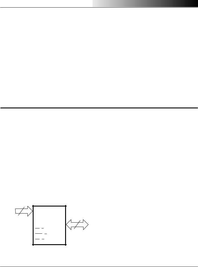
LOGIC SYMBOL
18
A0-A17
8
DQ0-DQ7
 CE (E)
 PGM (P)
 OE (G)
4 Integrated Silicon Solution, Inc.
EP019-0A 12/19/97
 Loading...