


Intel® CoreTM 2 Duo Processor
and Intel® Q45 Express Chipset
Development Kit
User’s Manual
October 2008
INFORMATION IN THIS DOCUMENT IS PROVIDED IN CONNECTION WITH INTEL® PRODUCTS. NO LICENSE, EXPRESS OR IMPLIED, BY
ESTOPPEL OR OTHERWISE, TO ANY INTELLECTUAL PROPERTY RIGHTS IS GRANTED BY THIS DOCUMENT. EXCEPT AS PROVIDED IN
INTEL’S TERMS AND CONDITIONS OF SALE FOR SUCH PRODUCTS, INTEL ASSUMES NO LIABILITY WHATSOEVER, AND INTEL DISCLAIMS
ANY EXPRESS OR IMPLIED WARRANTY, RELATING TO SALE AND/OR USE OF INTEL PRODUCTS INCLUDING LIABILITY OR WARRANTIES
RELATING TO FITNESS FOR A PARTICULAR PURPOSE, MERCHANTABILITY, OR INFRINGEMENT OF ANY PATENT, COPYRIGHT OR OTHER
INTELLECTUAL PROPERTY RIGHT. Intel products are not intended for use in medical, life saving, or life sustaining applications. Intel may make changes to specifications and product descriptions at any time, without notice.
Designers must not rely on the absence or characteristics of any features or instructions marked "reserved" or "undefined." Intel reserves these for future
definition and shall have no responsibility whatsoever for conflicts or incompatibilities arising from future changes to them.
The Eagle Lake chipset may contain design defects or errors known as errata which may cause the product to deviate from published specifications. Current
characterized errata are available on request.
Contact your local Intel sales office or your distributor to obtain the latest specifications and before placing your product order.
Intel and the Intel logo are trademarks or registered trademarks of Intel Corporation or its subsidiaries in the United States and other countries.
*Other names and brands may be claimed as the property of others. Copyright © 2008 Intel Corporation
All rights reserved.
2
Contents
1.0 About this Manual |
5 |
|||
|
1.1 |
Content Overview |
5 |
|
|
1.2 |
Text Conventions |
6 |
|
|
1.3 |
Glossary of Terms and Acronyms |
7 |
|
|
1.4 |
Support Options |
8 |
|
|
|
1.4.1 |
Electronic Support Systems |
8 |
|
|
1.4.2 |
Additional Technical Support |
8 |
|
1.5 |
Product Literature |
8 |
|
2.0 Development Kits Hardware Features |
9 |
|||
|
2.1 |
Intel® Q45 Development Kits Overview |
9 |
|
|
2.2 |
System Block diagram |
10 |
|
|
2.3 |
Development Kits Inventory Checklists |
11 |
|
|
2.4 |
Processor Supported |
12 |
|
|
2.5 |
System Memory |
12 |
|
|
|
2.5.1 |
Dual Channel (Interleaved) Mode Configurations |
13 |
|
|
2.5.2 |
Single Channel (Asymmetric) Mode Configurations |
15 |
|
2.6 |
Back-Panel Connector |
16 |
|
|
|
2.6.1 |
Audio-Connectors |
16 |
|
|
2.6.2 |
RJ-45 LAN Connector with Integrated LEDs |
17 |
|
|
2.6.3 |
USB Port |
17 |
|
|
2.6.5 |
HDMI Port |
17 |
|
2.7 |
Debug Features |
18 |
|
|
|
2.7.1 |
Extended Debug Probe (XDP) |
18 |
|
|
2.7.2 |
Power LEDs |
19 |
|
|
2.7.3 |
Port 80 POST Code LEDs |
19 |
|
|
2.7.4 |
Voltage Reference |
19 |
|
2.8 |
Development Kit’s Major connector and Jumper |
20 |
|
|
|
2.8.1 |
Jumper Functions |
20 |
|
|
2.8.2 |
USB 2.0 Front Panel |
21 |
|
|
2.8.3 |
1394a Header |
21 |
|
2.9 |
SPI Removal/Installation Technique |
23 |
|
|
|
2.9.1 |
SPI Device Installation |
23 |
|
|
2.9.2 |
SPI Device Removal |
26 |
3.0 |
Setting Up and configuring the development Kits |
27 |
||
|
3.1 |
Overview |
|
27 |
|
3.2 |
BTX Heatsink Setup |
28 |
|
|
|
3.2.1 |
SRM Alignment on any BTX board |
28 |
|
3.3 |
Board Setup and Configuration before Boot |
29 |
|
|
3.4 |
Post Codes Definitions |
31 |
|
4.0 |
BIOS Setup Utility |
35 |
||
|
4.1 |
Main |
|
35 |
|
|
4.1.1 |
System Overview |
35 |
|
4.2 |
Advance |
|
35 |
|
|
4.2.1 |
CPU Configuration |
35 |
|
|
4.2.2 |
IDE Configuration |
36 |
|
|
4.2.3 |
Floppy Configuration |
37 |
|
|
4.2.4 |
ACPI Configuration |
37 |
|
|
4.2.5 |
AHCI Configuration |
38 |
3
|
4.2.6 |
Intel AMT Configuration |
38 |
|
4.2.7 |
MPS Configuration |
39 |
|
4.2.8 |
SMBIOS Configuration |
39 |
|
4.2.9 |
Remote Access Configuration |
39 |
|
4.2.10 |
Trusted Computing |
39 |
|
4.2.11 |
USB Configuration |
40 |
4.3 |
PCIPnP |
|
40 |
4.4 |
Boot |
|
40 |
|
4.4.1 |
Boot setting Configuration |
40 |
4.5 |
Security |
|
41 |
4.6 |
Chipset |
|
41 |
|
4.6.1 |
Northbridge Configuration |
41 |
|
4.6.2 |
Southbridge Configuration |
43 |
|
4.6.3 |
ME System Configuration |
44 |
|
4.6.4 |
PCI Express Configuration |
46 |
|
4.6.5 |
VE Subsystem Configuration |
47 |
4.7 |
Virtual Appliance |
47 |
|
4.8 |
SV |
|
48 |
|
4.8.1 |
SV SMI Management |
48 |
|
4.8.2 |
SV SATA Management |
48 |
4.9 |
Exit |
|
49 |
4
1.0 About This Manual
This user’s manual describes the use of the Intel® Q45 Express Chipset Development Kit. This manual has been written for OEMs, system evaluators, and embedded system developers. All jumpers, headers, LED functions, and their locations on the board, along with subsystem features and POST codes, are defined in this document.
For the latest information about the Intel® Q45 Express Chipset Development Kit reference platform, visit:
http://developer.intel.com/design/intarch/devkits/index.htm?iid=embed_body+devkits
For design documents related to this platform, such as schematics and layout, please contact your Intel Representative.
1.1 Content Overview
Chapter 1: “About This Manual”
This chapter contains a description of conventions used in this manual. The last few sections explain how to obtain literature and contact customer support.
Chapter 2: “Development Kits Hardware Features”
This chapter provides information on the development kit features and the board capability. This includes the information on board component features, jumper settings, pin-out information for connectors and overall development kit board capability.
Chapter 3: “Development Kits Board ”
This chapter provides instructions on how to configure the evaluation board and
processor assembly by setting ATX heatsink, jumpers, connecting peripherals, providing power, and configuring the BIOS.
Chapter 4: “BIOS Setup Utility”
This chapter provides the BIOS function and how to configure the BIOS features. This include the BIOS option tab function like the Main System Overview, Advance, PCIPnP, Boot, Security, Chipset, SV, Exit.
5
1.2 Text Conventions
The following notations may be used throughout this manual.
#The pound symbol (#) appended to a signal name indicates that the signal is active low.
Variables |
Variables are shown in italics. Variables must be replaced with correct |
|
|
values. |
|
Instructions |
Instruction mnemonics are shown in uppercase. When you are |
|
|
programming, instructions are not case-sensitive. You may use either |
|
|
upper-case or lower-case. |
|
Numbers |
Hexadecimal |
numbers are represented by a string of hexadecimal |
|
digits followed by the character H. A zero prefix is added to numbers |
|
|
that begin with A through F. (For example, FF is shown as 0FFH.) |
|
|
Decimal and binary numbers are represented by their customary |
|
|
notations. (That is, 255 is a decimal number and 1111 1111 is a binary |
|
|
number.) In some cases, the letter B is added for clarity. |
|
Units of Measure |
The following abbreviations are used to represent units of measure: |
|
|
GByte |
gigabytes |
|
KByte |
kilobytes |
|
MByte |
megabytes |
|
MHz |
megahertz |
|
W |
watts |
|
V |
volts |
Signal Names |
Signal names are shown in uppercase. When several signals share a |
|
|
common name, an individual signal is represented by the signal name |
|
followed by a number, while the group is represented by the signal name followed by a variable (n). For example, the lower chip-select signals are named CS0#, CS1#, CS2#, and so on; they are collectively called CSn#. A pound symbol (#) appended to a signal name identifies an active-low signal. Port pins are represented by the port abbreviation, a period, and the pin number (e.g., P1.0).
6
1.3 Glossary of Terms and Acronyms
This section defines conventions and terminology used throughout this document.
Term |
Description |
|
|
ADD2 Card |
Advanced Digital Display Card – 2nd Generation. This card provides digital |
|
display options for an Intel Graphics Controller that supports ADD2+ cards. |
|
It plugs into a x16 PCI Express* connector but uses the multiplexed SDVO |
|
interface. The card adds Video In capabilities to platform. This Advanced |
|
Digital Display Card will not work with an Intel Graphics Controller that |
|
supports DVO and ADD cards. It will function as an ADD2 card in an ADD2 |
|
supported system, but video in capabilities will not work. T |
|
|
ACPI |
Advanced Configuration and Power Interface |
|
|
Core |
The internal base logic in the (G)MCH |
|
|
DDR3 |
A third generation Double Data Rate SDRAM memory technology |
|
|
DMI |
(G)MCH-Intel® ICH10 Direct Media Interface |
|
|
DVI |
Digital Video Interface. Specification that defines the connector and |
|
interface for digital displays. |
|
|
FSB |
Front Side Bus. FSB is synonymous with Host or processor bus |
|
|
GMA 4500 |
Intel® Graphic Media Accelerator 4500 |
|
|
Intel® ICH10 |
Ninth generation I/O Controller Hub component that contains additional |
|
functionality compared to previous ICHs. The I/O Controller Hub component |
|
contains the primary PCI interface, LPC interface, USB2, ATA-100, and other |
|
I/O functions. It communicates with the (G)MCH over a proprietary |
|
interconnect called DMI. |
|
|
IGD |
Internal Graphics Device. |
|
|
LVDS |
Low Voltage Differential Signaling. A high speed, low power data |
|
transmission standard used for display connections to LCD panels. |
|
|
MCH |
Memory Controller Hub component that contains the processor interface, |
|
DRAM controller, and x16 PCI Express* port (typically, the external graphics |
|
interface). It communicates with the I/O controller hub (Intel® ICH10) and |
|
other I/O controller hubs over the DMI interconnect. In this document MCH |
|
refers to the Intel® Q45 MCH component. |
|
|
MEC |
Media Expansion Card, also known as ADD2+ card. Refer to ADD2+ term for |
|
description. |
|
|
PCI Express* |
Third Generation input/output graphics attach called PCI Express* Graphics. |
|
PCI Express* is a high-speed serial interface whose configuration is software |
|
compatible with the existing PCI specifications. The specific PCI Express* |
|
implementation intended for connecting the (G)MCH to an external Graphics |
|
Controller is a x16 link and replaces AGP. |
|
|
Primary PCI |
The Primary PCI is the physical PCI bus that is driven directly by the ICH10 |
|
component. Communication between Primary PCI and the (G)MCH occurs |
|
over DMI. Note that the Primary PCI bus is not PCI Bus 0 from a |
|
configuration standpoint. |
|
|
7
Term |
Description |
|
|
SDVO |
Serial Digital Video Out (SDVO). SDVO is a digital display channel that |
|
serially transmits digital display data to an external SDVO device. The SDVO |
|
device accepts this serialized format and then translates the data into the |
|
appropriate display format (i.e., TMDS, LVDS, TV-Out). This interface is not |
|
electrically compatible with the previous digital display channel - DVO. For |
|
the 82Q965 GMCH, it will be multiplexed on a portion of the x16 graphics |
|
PCI Express* interface. |
|
|
SDVO Device |
Third party codec that uses SDVO as an input. May have a variety of output |
|
formats, including DVI, LVDS, HDMI, TV-out, etc. |
|
|
SMI |
System Management Interrupt. SMI is used to indicate any of several |
|
system conditions (such as, thermal sensor events, throttling activated, |
|
access to System Management RAM, chassis open, or other system state |
|
related activity). |
|
|
Rank |
A unit of DRAM corresponding to eight x8 SDRAM devices in parallel or four |
|
x16 SDRAM devices in parallel, ignoring ECC. These devices are usually, but |
|
not always, mounted on a single side of a DIMM. |
|
|
1.4 Support Options
1.4.1 Electronic Support Systems
Intel’s site on the World Wide Web (http://www.intel.com/) provides up-to-date technical information and product support. This information is available 24 hours per day, 7 days per week, providing technical information whenever you need it.
Product documentation is provided online in a variety of web-friendly formats at: http://developer.intel.com/literature/index.asp
1.4.2 Additional Technical Support
If you require additional technical support, please contact your field sales representative or local distributor.
1.5 Product Literature
Product literature can be ordered from the following Intel literature centers:
Location |
Telephone Number |
U.S. and Canada |
1-800-548-4725 |
U.S. (from overseas) |
708-296-9333 |
Europe (U.K.) |
44(0)1793-431155 |
Germany |
44(0)1793-421333 |
France |
44(0)1793-421777 |
Japan (fax only) |
81(0)120-47-88-32 |
Table 1: Intel Literature Centers
8

2.0 Development Kits Hardware Features
This chapter describes the development kit features of the Intel® Q45 Development Kits. These recommendations would largely apply to other designs incorporating Intel® Q45 chipset. This documentation should be used in conjunction with the Intel® Q45/ICH10 datasheet, specification updates and platform design guides. Contact your local Intel representative for the availability of these documents.
2.1Intel® Q45 Development Kits Overview
Figure 2-1 shows overview of the major features present on the development kit board. Refer to next page for system block diagram of the development kit’s motherboard.
|
2x2 |
|
Port 80 LED |
Standard |
|
display |
Power |
|
|
Supply |
|
PCI Slot |
|
|
|
LGA775 |
|
PCI Express |
Processor |
|
X1 slot |
Socket |
|
PCI Express |
|
|
X16 Graphic |
Intel® Q45 |
|
slot |
Memory |
|
|
Controller |
|
Power On |
Hub (MCH) |
|
|
||
button |
|
|
Intel® I/O |
|
|
Controller |
2-DIMM per |
|
Hub (ICH) |
channel DDR2 |
|
|
667/800 |
|
2-DIMM per |
(Channel-A) |
|
|
||
channel DDR2 |
|
|
667/800 |
2x12 Standard |
|
(Channel-B) |
||
Power Supply |
||
|
||
SATA Port |
|
Figure 2-1 Board Features
9

2.2System Block Diagram
This section will document the common features that are applicable to Intel® Q45 Express Chipset Development Kits. Figure 2-2 show a simple block diagram of the Intel® Q45 Express Chipset development kits.
|
|
|
|
|
|
|
|
|
|
|
|
|
|
|
|
|
|
|
|
LGA775 |
|
|
|
|
|
|
|
|
|
|
|
|
|
|
|
|
|
|
|
|
|
|
|
|||
|
|
|
|
|
|
|
|
|
|
|
|
|
|
|
|
|
|
|
|
Processor |
|
|
|
|
|
|
|
|
|
|
|
|
|
|
|
Clock |
|
|
||||||||
|
|
|
|
|
|
|
|
|
|
|
|
|
|
|
|
|
|
|
|
|
|
|
|
|
|
|
|
|
|
|
|
|
|
|
|
|
|
|
|
|
|
|
||||
SMBus Resume |
PCI Express |
X16 PCI Express |
|
|
|
|
|
|
|
|
|
|
|
|
|
|
|
|
|
|
|
|
|
SMBus Main |
||||||||||||||||||||||
|
|
Graphic |
|
|
|
|
|
|
|
|
|
1033 MT/s |
|
|
|
|
|
|
|
|
|
|
|
|
|
|
|
|
|
|
|
|
|
|
||||||||||||
|
|
|
|
|
|
|
X16 slot |
|
|
|
|
|
|
|
|
|
|
|
|
|
|
|
|
|
|
|
|
|
|
|
|
|
|
|
|
|
|
|
||||||||
|
|
|
|
|
|
|
(Primary) |
|
|
|
|
|
|
|
|
|
|
|
|
|
Dual |
|
|
|
|
|
|
|
|
|
DDR3 |
|
|
|
||||||||||||
|
|
|
|
|
|
|
|
|
|
|
|
|
|
|
|
|
|
|
|
|
|
|
|
|
|
|||||||||||||||||||||
|
|
|
|
|
|
|
|
|
|
|
|
|
|
|
|
|
|
|
|
|
|
|
|
|
|
|
|
|
|
|
|
|
|
|
|
|
|
|
|
|
|
|
||||
|
|
|
|
|
|
|
|
|
|
|
|
|
|
|
|
|
|
|
|
|
|
|
|
|
|
Channel |
|
|
|
|
|
|
|
|
|
|
|
|
|
|
|
|
|
|||
|
|
|
|
|
|
|
|
|
|
|
|
|
|
|
|
|
|
|
|
Graphics |
|
|
DDR3 |
|
|
|
|
|
|
|
|
|
|
|
|
|
|
|
|
|
||||||
|
|
|
|
|
|
|
|
|
|
|
|
|
|
|
|
|
|
|
|
|
1066 |
|
|
|
|
|
|
|
|
|
|
|
|
|
|
|
|
|
|
|
||||||
|
|
|
|
|
|
Integrated |
|
|
|
|
|
|
|
Memory |
|
|
|
|
|
|
|
|
|
|
|
|
|
|
|
|
|
|
|
|
||||||||||||
|
|
|
|
|
|
|
|
|
|
|
|
|
|
|
|
|
|
|
|
|
|
|
|
|
|
|
|
|
|
|
|
|
|
|
|
|||||||||||
|
|
|
|
|
Graphic VGA |
|
|
|
|
|
|
|
Controller Hub |
|
|
|
|
|
|
|
|
|
|
|
|
|
|
|
DDR3 |
|
|
|
||||||||||||||
|
|
|
|
|
|
|
Output |
|
|
|
|
|
|
|
|
|
|
|
|
|
|
|
|
|
|
|
|
|
|
|
|
|
|
|
|
|
|
|||||||||
|
|
|
|
|
|
|
|
|
|
|
|
|
|
|
|
|
|
|
|
(GMCH) |
|
|
|
|
|
|
|
|
|
|
|
|
|
|
|
|
|
|
|
|
|
|
|
|||
|
|
|
|
|
|
|
|
|
|
|
|
|
|
|
SP |
|
|
|
|
|
|
|
|
|
|
|
|
|
|
|
|
|
|
|
|
|
|
|
|
|
|
|
|
|||
|
|
|
|
|
|
|
|
|
|
|
|
|
|
|
Flash |
|
|
|
|
|
|
|
|
|
|
|
|
|
|
|
|
|
|
|
|
|
|
|
|
|
|
|
|
|||
|
|
|
|
|
|
|
|
|
|
|
|
|
|
Devic |
|
|
|
|
|
|
X1 PCI Express |
|
|
|
|
|
|
|
|
|
|
|
|
|
||||||||||||
|
|
|
|
SATA port 5 |
|
|
|
|
|
|
|
|
|
|
|
|
|
|
|
|
|
|
|
|
|
PCIE Slot |
|
|
|
|
|
|
|
|
|
|
||||||||||
|
|
|
|
|
|
|
|
|
|
|
|
|
|
|
|
|
|
|
|
|
|
|
|
|
|
|
|
|
|
|
|
|
|
|
||||||||||||
|
|
|
|
|
SATA port 4 |
|
|
|
|
|
|
SPI |
|
|
|
|
|
|
|
|
|
|
|
|
|
|
|
|
|
|
|
|
|
|
|
|
|
|
|
|||||||
|
|
|
|
|
SATA port 3 |
|
2 |
|
|
|
|
|
|
|
I/O Controller |
|
|
|
|
|
|
|
|
|
|
|
|
|
|
|
|
|
|
|
|
|
|
|
||||||||
|
|
|
|
|
|
|
|
|
|
|
|
|
|
|
|
|
|
|
|
|
|
|
|
|
|
|
|
|
|
|
|
|
|
|
|
|
|
|
||||||||
|
|
|
|
|
|
|
|
SATA port |
|
|
|
|
|
|
|
|
|
|
|
|
|
|
|
|
|
|
|
|
|
|
|
|
|
|
|
|
|
|
||||||||
|
|
|
|
|
|
|
|
|
SATA port 1 |
|
|
|
|
|
|
|
|
|
|
|
|
|
|
|
|
|
|
|
|
|
|
|
|
|
||||||||||||
|
|
|
|
|
|
|
|
|
|
|
|
|
|
|
|
|
|
|
|
|
|
|
|
|
|
|
|
|
|
|
|
|
|
|
|
|
|
|||||||||
|
|
|
|
|
|
|
|
|
|
SATA port 0 |
|
|
|
Hub |
|
|
|
PCI Bus |
|
|
|
|
|
|
|
|
|
|
|
|||||||||||||||||
|
|
|
|
|
|
|
|
|
|
|
|
|
|
|
|
|
|
|
|
|
(ICH) |
|
|
|
|
|
|
|
|
|
|
PCI Slot |
|
|
|
|
|
|
||||||||
|
|
|
|
|
|
|
|
|
|
|
|
|
|
|
|
|
|
|
|
|
|
|
|
|
|
|
|
|
|
|
|
|
|
|
|
|
|
|
|
|
|
|
|
|||
|
|
|
|
|
|
|
|
|
|
|
|
|
|
|
|
|
|
|
|
|
|
|
|
|
|
|
|
|
|
|
|
|
|
|
|
|
|
|
|
|
|
|
|
|||
|
|
|
|
|
|
|
|
|
|
|
|
|
|
|
|
|
|
|
|
|
|
|
|
|
|
|
|
|
|
|
|
|
|
|
|
|
|
|
|
|||||||
|
|
|
|
|
|
|
|
|
|
|
|
|
|
|
|
|
|
|
|
|
|
|
|
|
|
|
|
|
|
|
|
|
|
|
|
|
|
|
|
|
|
|
|
|
|
|
|
|
|
|
|
|
|
|
|
|
|
|
|
|
|
|
|
|
|
|
|
|
|
|
|
|
|
|
PCI |
|
SMBus Resume |
|
|||||||||||||||
|
|
|
|
|
|
|
|
|
|
|
|
|
|
|
|
|
|
|
|
|
|
|
|
|
|
|
1394 |
|
|
|
|
|
|
|
|
|
|
|
|
|||||||
|
|
|
|
|
|
|
|
|
|
|
|
|
|
|
|
|
|
|
|
USB 2.0 |
|
|
SMBus |
|
|
|
|
|
|
|
|
|
|
|
|
|||||||||||
|
|
|
|
|
|
|
|
|
|
|
|
|
|
|
|
|
|
|
|
|
|
|
|
|
|
|
|
|
|
|
|
|
||||||||||||||
|
|
|
|
|
|
|
|
|
|
|
|
|
|
|
|
|
|
|
|
|
|
|
|
|
|
|
|
|
|
|
|
|||||||||||||||
|
|
|
|
|
|
|
|
|
|
|
|
|
|
|
|
|
|
|
|
|
|
|
|
|
|
|
|
|
|
|
|
|
|
|
|
|
|
|
|
|
|
|
|
|
|
|
|
|
HD Audio |
|
|
|
|
|
|
|
|
|
|
|
|
|
|
|
|
|
|
|
|
|
|
|
|
|
|
|
|
|
|
|
|
|
|
|
|||||||||
|
|
|
|
|
|
|
|
|
|
|
|
|
|
|
|
|
|
|
Front Panel |
|
|
Back Panel |
|
|
|
|
|
|
|
|
|
|
|
|
|
|
|
|
|
|
|
|
|
|||
|
|
|
|
|
|
|
|
|
|
|
|
|
|
|
|
|
|
|
|
|
|
|
|
|
USB or LAN |
|
|
|
|
|
|
|
|
|
|
|
|
|||||||||
|
|
|
|
|
|
|
|
|
|
|
|
|
|
|
USB |
|
|
|
|
|
|
|
|
|
|
|
|
|
|
|
|
|
|
|
|
|
|
|
|
|
|
|
|
|
||
|
|
|
|
|
|
|
|
|
|
|
|
|
|
|
|
|
|
|
|
|
|
|
|
|
|
|
|
|
|
|
|
|
|
|
|
|
|
|
|
|
|
|
|
|
|
|
|
|
|
|
|
|
|
|
|
|
|
|
|
|
|
|
|
|
|
|
|
|
|
|
|
|
|
|
|
|
|
|
|
|
|
|
|
|
|
|
|
|
|
|
|
|
|
|
|
|
|
|
|
|
|
|
|
|
|
|
|
|
|
|
|
|
|
|
|
|
|
|
|
|
|
|
USB or 1394 |
|
|
|
|
|
|
|
|
|
|
|
|
|||||
|
|
|
|
|
|
|
|
|
|
|
|
|
|
|
|
|
|
|
|
|
|
|
|
|
|
|
|
|
|
|
|
|
|
|
|
|
|
|
|
|
||||||
|
|
|
|
|
|
|
|
|
|
|
|
|
|
|
|
|
|
|
|
|
|
|
|
|
|
|
|
|
|
|
|
|
|
|
|
|
|
|
|
|
|
|
|
|
|
|
|
|
|
|
|
|
|
|
|
|
|
|
|
|
|
|
|
|
|
|
|
|
|
|
|
|
|
|
|
|
|
|
|
|
|
|
|
|
|
|
|
|
|
|
|
|
|
|
|
|
|
|
|
|
|
|
|
|
|
|
|
|
|
|
|
|
|
|
|
|
|
|
|
|
|
|
|
|
|
|
|
|
|
|
|
|
|
|
|
|
|
|
|
|
|
|
|
|
|
|
|
|
|
|
|
|
|
|
|
|
|
|
|
|
|
|
|
|
|
|
|
|
|
|
USB |
|
|
|
|
|
|
|
|
|
|
|
|
||||
|
|
|
|
|
|
|
|
|
|
|
|
|
|
|
|
|
|
|
|
|
|
|
|
|
|
|
|
|
|
|
|
|
|
|
|
|
|
|
|
|
|
|
|
|
|
|
|
|
|
|
|
|
|
|
|
|
|
|
|
|
|
|
|
|
|
|
|
|
|
|
|
|
|
|
|
|
|
|
|
|
|
|
|
|
|
|
|
|
|
|
|
|
|
Figure 2-2 Intel® Q45 Development Kits block diagram.
10
2.3 Development Kits Inventory Checklists
Development Kits Inventory Checklists
This section descripts major hardware items which should be available on this development kits.
Development Kits Hardware Items
1x 4-Layer Micro-ATX form factor (targeted dimensions: 10.5” x 10.4”) motherboard
1x Intel® CoreTM 2 Duo E8400 Processors in the LGA775 Socket
2x 1 GBytes DDR3 800 DIMM
1x ATX Heatsink with fan
1x CD-ROM contain chipset drivers (this include Intel® GMA4500 driver)
Development Kits board Specification
1 PCI Express x16, 3 PCIe x1, 3 PCI expansion slots
1394a
o1 front panel headers for support of 1 port
o1 back panel port
Universal Serial Bus 2.0
o3 front panel headers for support of 6 ports
o6 back panel ports
6 SATA 3 Gb/sec ports
• Internal I/O headers
2x5 Front Panel I/O header
2x5 Front Panel audio header
1x2 Chassis intrusion header
3 four-wire fan headers
2x8 High Definition audio header
• Additional Features
5 Analog audio connectors and 1 high definition media interface (HDMI)
Piezo speaker for BIOS POST codes
BIOS configuration jumper
Clear CMOS jumper
Power Button
Reset Button
XDP connector
11
2.4 Processor Support
Intel® Q45 Development Kits support the following processors in the LGA775 Socket with FSB of 800/1067/1333 MHz. Processors listed here has long-life support and also supported by this development kits.
•Intel® CoreTM 2 Duo E8400 Series
•Intel® CoreTM 2 Duo E6400 Series
•Intel® CoreTM 2 Duo E4300 Series
•Intel® Celeron 440
Refer to this link for other processors which is also supported by Intel® Q45 Express Chipset. http://developer.intel.com/products/chipsets/Q35_Q33/index.htm
2.5 System Memory
The Intel® Q45 MCH supports two types of memory organization. These are interleaved mode and asymmetric mode. Listed here are the summary of the system memory supported.
•Non-ECC DDR3 (800/1066)
•512Mb, 1Gb and 2Gb technology
•4 DIMMs, 8GB maximum per channel, 16GB total memory
•Dual channel (Interleaved) mode. This mode offers the highest throughput for real world applications. Dual channel mode is enabled when the installed memory capacities of both DIMM channels are equal. Technology and device width can vary from one channel to the other but the installed memory capacity for each channel must be equal. If different speed DIMMs is used between channels, the slowest memory timing will be used.
•Single channel (Asymmetric) mode. This mode is equivalent to single channel bandwidth operation for real world applications. This mode is used when only a single DIMM is installed or the memory capacities are unequal. Technology and device width can vary from one channel to the other. If different speed DIMMs is used between channels, the slowest memory timing will be used.
Figure 2-3 illustrates the memory channel and DIMM configuration.
12
Channel A DIMM 0
Channel A DIMM 1
Channel B DIMM 0
Channel B DIMM 1
Figure 2-3 Memory Channel and DIMM Configuration
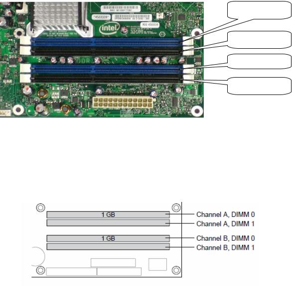
2.5.1 Dual Channel (Interleaved) Mode Configurations
Figure 2-4 shows a dual channel configuration using two DIMMs. In this example, the DIMM 0 sockets of both channels are populated with identical DIMMs.
Figure 2-4: Dual Channel (Interleaved) Mode Configuration with 2x DIMMs
13
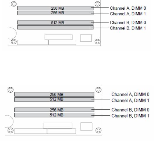
Figure 2-5 shows a dual channel configuration using 3 DIMMs. In this example, the combined capacity of the two DIMMs in Channel A equal the capacity of the single DIMM in the DIMM 0 socket of Channel B.
Figure 2-5: Dual Channel (Interleaved) Mode Configuration with 3x DIMMs
Figure 2-6 shows a dual channel configuration using 4 DIMMs. In this example, the combined capacity of the 2x DIMMs in Channel A equals the combined capacity of the 2x DIMMs in Channel B. Also, the DIMMs are matched between DIMM 0 and DIMM 1 of both channels.
Figure 2-6: Dual Channel (Interleaved) Mode Configuration with 4x DIMMs
14
2.5.2 Single Channel (Asymmetric) Mode Configurations
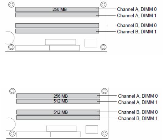
Figure 2.7 shows a single channel configuration using 1x DIMM. In this example, only the DIMM 0 socket of Channel A is populated. Channel B is not populated.
Figure 2.7: Single Channel (Asymmetric) Mode Configuration with 1x DIMM
Figure 2.8 shows a single channel configuration using 3x DIMMs. In this example, the combined capacity of the 2x DIMMs in Channel A does not equal the capacity of the single DIMM in the DIMM 0 socket of Channel B.
Figure 2.8: Single Channel (Asymmetric) Mode Configuration with 3x DIMMs
15
 Loading...