


MI940
LGA775 Core™ 2 Duo
Intel® 945GC Chipset
Mini-ITX Motherboard
USER’S MANUAL
Version 1.0

Acknowledgments
Award is a registered trademark of Award Software International, Inc.
PS/2 is a trademark of International Business Machines Corporation.
Intel is a trademark or registered trademark of Intel Corporation. Microsoft Windows is a registered trademark of Microsoft Corporation.
Winbond is a registered trademark of Winbond Electronics Corporation.
All other product names or trademarks are properties of their respective owners.

Table of Contents |
|
Introduction ....................................................... |
1 |
Checklist.............................................................................. |
1 |
Product Description............................................................. |
2 |
Specifications ...................................................................... |
3 |
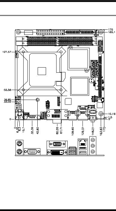
Board Dimensions ............................................................... |
4 |
Installations ....................................................... |
5 |
Installing the CPU ............................................................... |
6 |
ATX Power Installation ...................................................... |
6 |
Installing the Memory ......................................................... |
7 |
Setting the Jumpers ............................................................. |
8 |
Connectors on MI940........................................................ |
11 |
BIOS Setup....................................................... |
21 |
Drivers Installation ...................................... |
43 |
Intel Chipset Software Installation Utility......................... |
44 |
VGA Drivers Installation .................................................. |
47 |
High Definition Codec Audio Driver Installation............. |
49 |
LAN Drivers Installation................................................... |
51 |
Appendix ........................................................... |
53 |
A. I/O Port Address Map................................................... |
53 |
B. Interrupt Request Lines (IRQ)...................................... |
54 |
C. Watchdog Timer Configuration.................................... |
55 |
MI940 User’s Manual |
iii |

This page is intentionally left blank.
iv |
MI940 User’s Manual |

INTRODUCTION
Introduction
Checklist
Your MI940 Core 2 Duo motherboard package should include the items listed below:
•The MI940 motherboard
•This User’s manual
•1 x I/O shield
•1 x IDE cable
•1 x SATA cable
•1 CD containing the following:
•Chipset Drivers
•Flash Memory Utility
MI940 User’s Manual |
1 |

INSTALLATIONS
Product Description
The MI940 Mini-ITX motherboard is designed for LGA775 processors such as the Intel® Core™2 Duo, and Pentium D / Pentium 4 processors with up to 800MHz FSB. It is based on the Intel’s 945GC Express chipset and it comes with two DDR2 memory slots and 2GB memory capacity for faster system responsiveness.
MI940 comes with the Intel® 945GC integrated graphics and Chrontel CH7307 to support for CRT and DVI display interface. LAN functionality is supported with a Gigabit Ethernet controller.
MI940 is expandable, with the use of an adaptor card, ID394, to support more serial ports, or ID395 to support TPM 1.2 security function. Other useful features on the board include four SATA II ports, six USB 2.0 ports, watchdog timer, digital I/O and two serial ports. Board dimensions are 170mm by 170mm.
MI940 FEATURES
yIntel® 945GC Express Chipset Based
ySupport LGA775 Intel® Core™2 Duo/ Pentium D/Pentium 4 CPU
ySupport up to 800MHz FSB
ySupport up to 2GB DDRII 400/533/667 memory
y1 x PCI Express (x1)
y1 x PCI (supports 2 Master)
ySupport one Gigabit LAN on board
y4x SATA II, 1x IDE, 6x USB 2.0,
2x COM, 5.1Ch.HD Audio
2 |
MI940 User’s Manual |

|
|
INTRODUCTION |
|
|
|
|
|
|
|
|
|
|
Specifications |
|
|
|
|
|
|
|
|
|
|
|
Form Factor |
Mini ITX (for performance desktop market) |
|
|
Processor |
Socket LGA775, Supports the Intel Core 2 Duo and Intel Pentium D |
|
|
|
processors. |
|
|
FSB |
533/800 MHz |
|
|
Chipset |
Intel 945GC Chipset: |
|
|
|
• Intel 945GC Graphic Memory Controller Hub (GMCH) |
|
|
|
• Intel ICH7 I/O Controller Hub |
|
|
BIOS |
• Award BIOS: footprint from SPI, supports ACPI, SMBIOS |
|
|
Memory |
• 2 x 240-pin DDRII 400/533/667 DIMM sockets, support dual |
|
|
|
channels, |
|
|
|
• Supports max. 2 GB system memory |
|
|
VGA |
Intel 945GC integrated graphic subsystem (GMA950) |
|
|
DVI |
Chrontel CH7307C DVI transmitter |
|
|
LAN |
Intel 82574L PCI-express Gigabit LAN controller x1 |
|
|
USB |
Intel ICH7 built-in USB 2.0 host controller, supports 6 ports: |
|
|
|
•4 ports in the rear I/O region |
|
|
|
•2 ports with on-board headers |
|
|
SATA II |
Intel ICH7 built-in SATA II controller (3.0Gb/sec) w/ 4 ports |
|
|
IDE |
Intel ICH7 built-in IDE controller, supports Ultra ATA100/66/33 |
|
|
Audio |
Intel ICH7 built-in high definition audio w/ Realtek ALC662 Codec |
|
|
LPC I/O |
Winbond W83627EHG: COM1 (RS232), COM2 (RS232/422/485) & |
|
|
|
Hardware monitor |
|
|
Hardware Monitor |
• Three fan connectors with tachometer support |
|
|
|
• CPU fan connector supports 4-wire fan with PWM control |
|
|
|
• Supports two thermal diodes (CPU die + 1 on-board) |
|
|
|
• Voltage monitoring for VCC (processor), 3.3V, 5V, and 12V |
|
|
Edge Connectors |
• Mini-DIN x1 for PS/2 KB & MS |
|
|
|
• DB9 connector x1 for COM1 |
|
|
|
• DB15 & DVI-D stack connector x1 for VGA and DVI |
|
|
|
• RJ45 + dual USB stack connector x1 for LAN and USB1-2 |
|
|
|
• Dual USB connector x1 for USB3-4 |
|
|
|
• Triple (3x1) phone jack connector x1 for High-Definition Audio |
|
|
On Board Headers / |
• Standard SATA (7-pin shrouded vertical) connector x4 |
|
|
Connectors |
• 4x2 pins pin-header x1 for USB 5-6 |
|
|
|
• 5x2 pins DF11-10 x1 for COM2 (RS232/422/485) |
|
|
|
• 5x2 pins pin-header x1 for Digital I/O |
|
|
|
• 5X2 pins pin-headerx1 for audio front. |
|
|
|
• 40 pins box-header x1 for IDE |
|
|
|
• 4 pins pin--header x1 for CPU fan & system fan |
|
|
|
• 3 pins pin--header x2 for system fan |
|
|
Expansion |
PCI-express (x1) slot x1 |
|
|
|
PCI slot x1 (supports 2 master) |
|
|
|
8x2 pins pin header x1 for adaptor card: |
|
|
|
- ID394 (2 or 4 serial ports) |
|
|
|
- ID395 (TPM function) |
|
|
Watchdog Timer |
Yes (256 segments, 0, 1, 2…255 sec/min) |
|
|
Digital IO |
4 in and 4 Out |
|
|
Other |
LAN Wakeup |
|
|
Power Connector |
24 pins ATX main power + 4 pins 12V |
|
|
System Voltage |
+5V, +3.3V, +12V, -12V & 5VSB |
|
|
Board Size |
170 x 170mm |
|
MI940 User’s Manual |
3 |
INSTALLATIONS
Board Dimensions
4 |
MI940 User’s Manual |

INSTALLATIONS
Installations
This section provides information on how to use the jumpers and connectors on the MI940 in order to set up a workable system. The topics covered are:
Installing the CPU ................................................................................. |
6 |
ATX Power Installation......................................................................... |
6 |
Installing the Memory ........................................................................... |
7 |
Setting the Jumpers................................................................................ |
8 |
Connectors on MI940.......................................................................... |
11 |
MI940 User’s Manual |
5 |
INSTALLATIONS
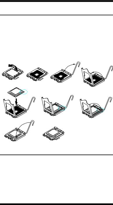
Installing the CPU
The MI940 motherboard supports an LGA 775 processor socket for Intel® Core 2 Duo processors.
The LGA 775 processor socket comes with a lever to secure the processor. Refer to the pictures below, from left to right, on how to place the processor into the CPU socket. Please note that the cover of the
LGA775 socket must always be installed during transport to avoid damage to the socket.
ATX Power Installation
The system power is provided to the motherboard with the ATX2 and ATX1 power connectors. ATX2 is a 24-pin power connector and ATX1 is a 4-pin 12V power connector.
The 24-pin power connector can to be connected to a standard 20-pin ATX power connector in a standard ATX power supply (Min. 400watt).
Note: The power supply 5VSB voltage must be at least 2A.
6 |
MI940 User’s Manual |
INSTALLATIONS
Installing the Memory
The MI940 motherboard supports four DDR2 memory sockets for a maximum total memory of 2GB in DDR memory type. It supports DDR2 400/533/667MHz.
Basically, the system memory interface has the following features: Supports two 64-bit wide DDR data channels
Available bandwidth up to 5.3GB/s (DDR2 667) for single channel mode and 10.6GB/s (DDR2 667) for dual channel mode.
Supports 256Mb, 512Mb, 1Gb DDR2 technologies. Supports only x8, x16, DDR2 devices with four banks Supports only unbuffered DIMMs
Supports opportunistic refresh
Up to 32 simultaneously open pages (four per row, four rows maximum)
MI940 User’s Manual |
7 |

INSTALLATIONS
Setting the Jumpers
Jumpers are used on the motherboard are used to select various settings and features according to your needs and applications. Contact your supplier if you have doubts about the best configuration for your needs. The following lists the connectors and their respective functions.
Jumper Locations on MI940 .................................................................. |
9 |
JP5: Clear CMOS Contents ................................................................. |
10 |
JP1, JP2, JP3: RS232/422/485 (COM2) Selection .............................. |
10 |
8 |
MI940 User’s Manual |
INSTALLATIONS
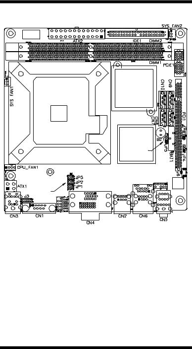
Jumper Locations on MI940
Jumper Locations on MI940......................................................Page |
JP1, JP2, JP3: RS232/422/485 (COM2) Selection....................... 10 |
JP5: Clear CMOS Contents .......................................................... 10 |
MI940 User’s Manual |
9 |
INSTALLATIONS
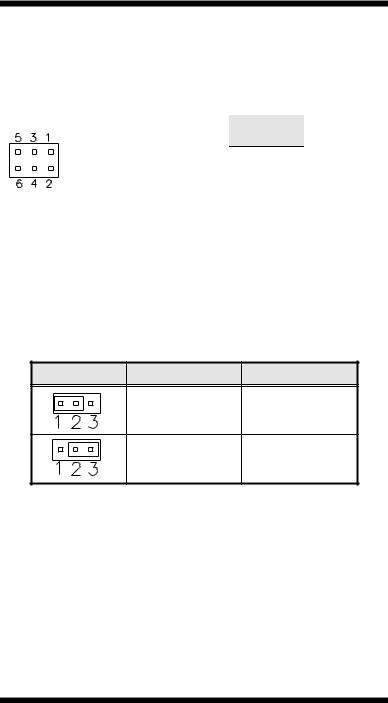
JP1, JP2, JP3: RS232/422/485 (COM2) Selection
COM1 is fixed for RS-232 use only.
COM2 is selectable for RS232, RS-422 and RS-485.
ID394: COM3 and COM4 are fixed for RS-232 use only. The following table describes the jumper settings for COM2 selection.
COM2 |
RS-232 |
RS-422 |
RS-485 |
|
Function |
||||
|
JP3: |
|
||
|
JP3: |
JP3: |
||
Jumper |
1-2 |
3-4 |
5-6 |
|
|
|
|
||
Setting |
JP1: |
JP1: |
JP1: |
|
(pin closed) |
3-5 & 4-6 |
1-3 & 2-4 |
1-3 & 2-4 |
|
|
JP2: |
JP2: |
JP2: |
|
|
3-5 & 4-6 |
1-3 & 2-4 |
1-3 & 2-4 |
JP5: Clear CMOS Contents
Use JP5, a 3-pin header, to clear the CMOS contents. Note that the ATX-power connector should be disconnected from the motherboard before clearing CMOS.
JP5 |
Setting |
Function |
|
Pin 1-2 |
Normal |
|
Short/Closed |
|
|
|
|
|
Pin 2-3 |
Clear CMOS |
|
Short/Closed |
|
|
|
10 |
MI940 User’s Manual |

INSTALLATIONS
Connectors on MI940
The connectors on MI940 allow you to connect external devices such as keyboard, floppy disk drives, hard disk drives, printers, etc. The following table lists the connectors on MI940 and their respective functions.
Connector Locations on MI940 ....................................................................... |
12 |
ATX2: 24-pin ATX Power Connector............................................................. |
13 |
ATX1: ATX 12V Power Connector ................................................................ |
13 |
CPU_FAN1: CPU Fan Power Connector ....................................................... |
13 |
SYS FAN1, 2: System Fan Power Connectors ................................................ |
13 |
CN3: PS/2 Keyboard and PS/2 Mouse Connectors ......................................... |
14 |
CN1, J1: COM1/2 Serial Ports......................................................................... |
14 |
CN4: VGA & DVI-D Connector ..................................................................... |
15 |
CN2: USB2/3 Connector ................................................................................. |
15 |
CN5: Audio Connector .................................................................................... |
15 |
CN6: Intel 82574L PCI-express Gigabit LAN and USB0/1 Connector........... |
16 |
CN7, CN8, CN9, CN10: SATA HDD Connectors .......................................... |
16 |
IDE1: Primary IDE Connectors....................................................................... |
16 |
J3: Digital I/O Connector (4 in, 4 out)............................................................. |
17 |
J4: Audio Front Header ................................................................................... |
17 |
J5: For LPC I/F Adaptor Card ......................................................................... |
17 |
J6: SPDIF Out Connector ................................................................................ |
17 |
J7: System Function Connector ....................................................................... |
17 |
J8: USB4/5 Connectors.................................................................................... |
18 |
J9: Power LED................................................................................................. |
18 |
PCIE1: x1 PCI Express Slot ............................................................................ |
18 |
PCI1: PCI Slot (supports 2 master)................................................................. |
18 |
ID394 LPC Serial Ports Adapter (option)........................................................ |
19 |
MI940 User’s Manual |
11 |

INSTALLATIONS
Connector Locations on MI940
ATX2: 24-pin ATX Power Connector ................................................................................................... |
13 |
ATX1: ATX 12V Power Connector ....................................................................................................... |
13 |
CPU_FAN1: CPU Fan Power Connector.............................................................................................. |
13 |
SYSFAN1, 2: System Fan Power Connectors........................................................................................ |
13 |
CN3: PS/2 Keyboard and PS/2 Mouse Connectors ............................................................................... |
14 |
CN1, J1: COM1/2 Serial Ports ............................................................................................................... |
14 |
CN4: VGA CRT and DVI-D Connector ................................................................................................ |
15 |
CN6: Intel 82574L PCI-express Gigabit LAN and USB0/1 Connector ................................................ |
16 |
CN2: USB2/3 Connector ........................................................................................................................ |
15 |
CN5: Audio Connector ........................................................................................................................... |
15 |
CN7, CN8, CN9, CN10: SATA HDD Connectors................................................................................. |
16 |
IDE1: Primary IDE Connectors.............................................................................................................. |
16 |
J3: Digital I/O Connector (4 in, 4 out) ................................................................................................... |
17 |
J5: For LPC I/F Adaptor Card ................................................................................................................ |
17 |
J4: Audio Front Header .......................................................................................................................... |
17 |
J8: USB4/5 Connectors........................................................................................................................... |
17 |
J9: Power LED........................................................................................................................................ |
18 |
J6: SPDIF Out Connector ....................................................................................................................... |
17 |
J7: System Function Connector.............................................................................................................. |
17 |
12 |
MI940 User’s Manual |
|
|
|
INSTALLATIONS |
ATX2: 24-pin ATX Power Connector |
|
||
Signal Name |
Pin # |
Pin # |
Signal Name |
3.3V |
13 |
1 |
3.3V |
-12V |
14 |
2 |
3.3V |
Ground |
15 |
3 |
Ground |
PS-ON |
16 |
4 |
+5V |
Ground |
17 |
5 |
Ground |
Ground |
18 |
6 |
+5V |
Ground |
19 |
7 |
Ground |
-5V |
20 |
8 |
Power good |
+5V |
21 |
9 |
5VSB |
+5V |
22 |
10 |
+12V |
+5V |
23 |
11 |
+12V |
Ground |
24 |
12 |
+3.3V |
ATX1: ATX 12V Power Connector
This connector supplies the CPU operation voltage
Pin # |
Signal Name |
1 |
Ground |
2 |
Ground |
3 |
+12V |
4 |
+12V |
CPU_FAN1: CPU Fan Power Connector |
|
Pin # |
Signal Name |
1 |
Ground |
2 |
+12V |
3 |
Sense |
4 |
Control |
SYS FAN1, 2: System Fan Power Connectors |
|
Pin # |
Signal Name |
1 |
Ground |
2 |
+12V |
3 |
Sense |
MI940 User’s Manual |
13 |
INSTALLATIONS
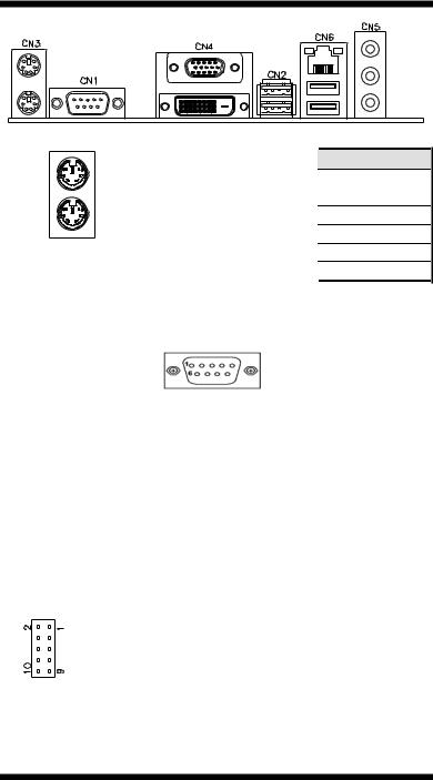
CN3: PS/2 Keyboard and PS/2 Mouse Connectors
Mouse (top)
Keyboard (bottom)
Keyboard Signal |
Pin # |
Mouse Signal |
Keyboard data |
1 |
Mouse data |
N.C. |
2 |
N.C. |
GND |
3 |
GND |
5V |
4 |
5V |
Keyboard clock |
5 |
Mouse clock |
N.C. |
6 |
N.C. |
CN1, J1: COM1/2 Serial Ports
CN1 (COM1) is a DB-9 connector, while J1 is a COM pin-header connector.
Signal Name |
Pin # |
Pin # |
Signal Name |
DCD, Data carrier detect |
1 |
6 |
DSR, Data set ready |
RXD, Receive data |
2 |
7 |
RTS, Request to send |
TXD, Transmit data |
3 |
8 |
CTS, Clear to send |
DTR, Data terminal ready |
4 |
9 |
RI, Ring indicator |
GND, ground |
5 |
10 |
Not Used |
J1: COM2 is jumper selectable for RS-232, RS-422 and RS-485.
Pin # |
|
Signal Name |
|
|
|
RS-232 |
R2-422 |
|
RS-485 |
1 |
DCD |
TX- |
|
DATA- |
2 |
RX |
TX+ |
|
DATA+ |
3 |
TX |
RX+ |
|
NC |
4 |
DTR |
RX- |
|
NC |
5 |
Ground |
Ground |
|
Ground |
6 |
DSR |
NC |
|
NC |
7 |
RTS |
NC |
|
NC |
8 |
CTS |
NC |
|
NC |
9 |
RI |
NC |
|
NC |
10 |
NC |
NC |
|
NC |
14 |
MI940 User’s Manual |
INSTALLATIONS
CN4: VGA & DVI-D Connector |
Signal Name |
Pin # |
Pin # |
Signal Name |
Red |
1 |
2 |
Green |
Blue |
3 |
4 |
N.C. |
GND |
5 |
6 |
GND |
GND |
7 |
8 |
GND |
VCC |
9 |
10 |
GND |
N.C. |
11 |
12 |
DDCDATA |
HSYNC |
13 |
14 |
VSYNC |
DDCCLK |
15 |
|
|
Signal Name |
Pin # |
Pin # |
Signal Name |
DATA2- |
1 |
2 |
DATA2+ |
GND |
3 |
4 |
N.C. |
N.C. |
5 |
6 |
DDCCLK |
DDCDATA |
7 |
8 |
N.C. |
DATA1- |
9 |
10 |
DATA1+ |
GND |
11 |
12 |
N.C. |
N.C. |
13 |
14 |
VCC |
GND |
15 |
16 |
Hot Plug |
|
|
|
Detect |
DATA0- |
17 |
18 |
DATA0+ |
GND |
19 |
20 |
N.C. |
N.C. |
21 |
22 |
GND |
CLK+ |
23 |
24 |
CLK- |
CN2: USB2/3 Connector
CN5: Audio Connector
CN5 is a 3-jack audio connector.
MI940 User’s Manual |
15 |
INSTALLATIONS
CN6: Intel 82574L PCI-express Gigabit LAN and USB0/1
Connector
CN7, CN8, CN9, CN10: SATA HDD Connectors
Pin # |
Signal Name |
1 |
Ground |
2 |
TX+ |
3 |
TX- |
4 |
Ground |
5 |
RX- |
6 |
RX+ |
7 |
Ground |
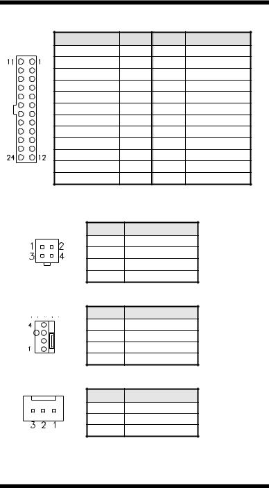
IDE1: Primary IDE Connectors |
|
|
|||||
|
|
|
|
Signal Name |
Pin # |
Pin # |
Signal Name |
|
|
|
|
Reset IDE |
1 |
2 |
Ground |
|
|
|
|
Host data 7 |
3 |
4 |
Host data 8 |
|
|
|
|
Host data 6 |
5 |
6 |
Host data 9 |
|
|
|
|
Host data 5 |
7 |
8 |
Host data 10 |
|
|
|
|
Host data 4 |
9 |
10 |
Host data 11 |
|
|
|
|
Host data 3 |
11 |
12 |
Host data 12 |
|
|
|
|
Host data 2 |
13 |
14 |
Host data 13 |
|
|
|
|
Host data 1 |
15 |
16 |
Host data 14 |
|
|
|
|
Host data 0 |
17 |
18 |
Host data 15 |
|
|
|
|
Ground |
19 |
20 |
Protect pin |
|
|
|
|
DRQ0 |
21 |
22 |
Ground |
|
|
|
|
Host IOW |
23 |
24 |
Ground |
|
|
|
|
Host IOR |
25 |
26 |
Ground |
|
|
|
|
IOCHRDY |
27 |
28 |
Host ALE |
|
|
|
|
DACK0 |
29 |
30 |
Ground |
|
|
|
|
IRQ14 |
31 |
32 |
No connect |
|
|
|
|||||
IDE1 |
|
|
|
|
|
||
|
Address 1 |
33 |
34 |
No connect |
|||
|
|
|
|
Address 0 |
35 |
36 |
Address 2 |
|
|
|
|
Chip select 0 |
37 |
38 |
Chip select 1 |
|
|
|
|
Activity |
39 |
40 |
Ground |
16 |
MI940 User’s Manual |
 Loading...