


 Loading...
R
Intel® 820E Chipset
Design Guide
May 2001
Document Number: 298187-003

Intel® 820E Chipset
R
Information in this document is provided in connection with Intel® products. No license, express or implied, by estoppel or otherwise, to any intellectual property rights is granted by this document. Except as provided in Intel’s Terms and Conditions of Sale for such products, Intel assumes no liability whatsoever, and Intel disclaims any express or implied warranty, relating to sale and/or use of Intel products including liability or warranties relating to fitness for a particular purpose, merchantability, or infringement of any patent, copyright or other intellectual property right. Intel products are not intended for use in medical, life saving, or life sustaining applications.
Intel may make changes to specifications and product descriptions at any time, without notice.
Designers must not rely on the absence or characteristics of any features or instructions marked "reserved" or "undefined." Intel reserves these for future definition and shall have no responsibility whatsoever for conflicts or incompatibilities arising from future changes to them.
The Intel® 820E Chipset may contain design defects or errors known as errata which may cause the product to deviate from published specifications. Current characterized errata are available on request.
Contact your local Intel sales office or your distributor to obtain the latest specifications and before placing your product order.
I2C is a two-wire communications bus/protocol developed by Philips. SMBus is a subset of the I2C bus/protocol and was developed by Intel. Implementations of the I2C bus/protocol may require licenses from various entities, including Philips Electronics N.V. and North American Philips Corporation.
Alert on LAN is a result of the Intel-IBM Advanced Manageability Alliance and a trademark of IBM
Copies of documents that have an ordering number and are referenced in this document, or other Intel literature, may be obtained from: Intel Corporation
www.intel.com
or call 1-800-548-4725
Intel, Pentium III, Pentium II, PentiumPro, Celeron, and MMX are trademarks or registered trademarks of Intel Corporation or its subsidiaries in the United States and other countries.
*Other names and brands may be claimed as the property of others.
2 |
Design Guide |

Intel® 820E Chipset
R
Contents
1. |
Introduction ................................................................................................................................ |
|
|
13 |
|
|
1.1. |
About This Design Guide .............................................................................................. |
13 |
||
|
1.2. |
Reference Documents................................................................................................... |
14 |
||
|
1.3. |
System Overview........................................................................................................... |
|
15 |
|
|
|
1.3.1. |
Chipset Components................................................................................... |
16 |
|
|
|
1.3.2. |
Bandwidth Summary ................................................................................... |
17 |
|
|
|
1.3.3. |
System Configuration .................................................................................. |
18 |
|
|
1.4. |
Platform Initiatives ......................................................................................................... |
|
20 |
|
|
|
1.4.1. |
Direct Rambus RAM (RDRAM*) ................................................................. |
20 |
|
|
|
1.4.2. |
Streaming SIMD Extensions ....................................................................... |
20 |
|
|
|
1.4.3. |
AGP 2.0 ...................................................................................................... |
20 |
|
|
|
1.4.4. |
Hub Interface............................................................................................... |
20 |
|
|
|
1.4.5. |
Integrated LAN Controller............................................................................ |
21 |
|
|
|
1.4.6. |
Ultra ATA/100 Support ................................................................................ |
21 |
|
|
|
1.4.7. |
Expanded USB Support .............................................................................. |
21 |
|
|
|
1.4.8. |
Manageability .............................................................................................. |
21 |
|
|
|
1.4.9. |
AC’97 |
........................................................................................................ |
23 |
|
|
1.4.10. |
Low-Pin-Count (LPC) Interface ................................................................... |
25 |
|
2. |
Layout/Routing Guidelines ......................................................................................................... |
|
27 |
||
|
2.1. |
General Recommendations........................................................................................... |
27 |
||
|
2.2. |
Component Quadrant Layout ........................................................................................ |
27 |
||
|
2.3. |
Intel® 820E Chipset Component Placement.................................................................. |
29 |
||
|
2.4. |
Core Chipset Routing Recommendations..................................................................... |
30 |
||
|
2.5. |
Source-Synchronous Strobing....................................................................................... |
32 |
||
|
2.6. |
Differential Clocking/Strobing ........................................................................................ |
33 |
||
|
2.7. |
Direct RDRAM* Interface .............................................................................................. |
33 |
||
|
|
2.7.1. |
Stack-Up...................................................................................................... |
34 |
|
|
|
2.7.2. |
Direct RDRAM* Layout Guidelines.............................................................. |
34 |
|
|
|
|
2.7.2.1. |
RSL Routing ................................................................................... |
35 |
|
|
|
2.7.2.2. |
RSL Termination............................................................................. |
38 |
|
|
|
2.7.2.3. Direct RDRAM* Ground Plane Reference...................................... |
39 |
|
|
|
|
2.7.2.4. Direct RDRAM* Connector Compensation..................................... |
41 |
|
2.7.2.4.1.Direct RDRAM* Channel Connector Compensation
|
|
|
Enhancement Recommendation.................................. |
47 |
|
|
2.7.2.5. RSL Signal Layer Alternation.......................................................... |
49 |
|
|
|
2.7.2.6. |
Length Matching Methods .............................................................. |
50 |
|
|
2.7.2.7. |
Via Compensation .......................................................................... |
52 |
|
|
2.7.2.8. Length Matching and Via Compensation Example......................... |
52 |
|
|
2.7.3. |
Direct RDRAM* Reference Voltage............................................................. |
54 |
|
|
2.7.4. |
High-Speed CMOS Routing ........................................................................ |
54 |
|
|
|
2.7.4.1. |
SIO Routing .................................................................................... |
55 |
|
|
2.7.4.2. |
Suspend-to-RAM Shunt Transistor................................................. |
56 |
|
2.7.5. |
Direct RDRAM* Clock Routing.................................................................... |
57 |
|
|
2.7.6. |
Direct RDRAM* Design Checklist ............................................................... |
57 |
|
2.8. |
AGP 2.0......................................................................................................................... |
|
60 |
|
|
2.8.1. |
AGP Interface Signal Groups...................................................................... |
60 |
|
|
2.8.2. |
1× Timing Domain Routing Guidelines........................................................ |
62 |
|
Design Guide |
3 |

Intel® 820E Chipset
|
|
|
|
|
|
|
|
|
R |
|
|
|
|
|
|
|
|
|
|
|
2.8.3. |
2×/4× Timing Domain Routing Guidelines ................................................... |
62 |
||||||
|
2.8.4. |
AGP 2.0 Routing Summary ......................................................................... |
64 |
||||||
|
2.8.5. |
AGP Clock Routing...................................................................................... |
65 |
||||||
|
2.8.6. |
General AGP Routing Guidelines ................................................................ |
65 |
||||||
|
|
2.8.6.1. |
Recommendations .......................................................................... |
65 |
|||||
|
2.8.7. |
VDDQ Generation and TYPEDET#................................................................ |
66 |
||||||
|
2.8.8. |
VREF Generation for AGP 2.0 (2× and 4×).................................................... |
68 |
||||||
|
2.8.9. |
Compensation.............................................................................................. |
70 |
||||||
|
2.8.10. |
AGP Pull-Ups............................................................................................... |
70 |
||||||
|
|
2.8.10.1. |
AGP Signal Voltage Tolerance List................................................. |
71 |
|||||
|
2.8.11. |
Motherboard / Add-in Card Interoperability.................................................. |
71 |
||||||
|
2.8.12. |
AGP Universal Retention Mechanism (RM) ................................................ |
72 |
||||||
2.9. |
Hub Interface ................................................................................................................. |
|
74 |
||||||
|
2.9.1. |
8-Bit Hub Interface Routing Guidelines ....................................................... |
75 |
||||||
|
|
2.9.1.1. |
8-Bit Hub Interface Data Signals..................................................... |
75 |
|||||
|
|
2.9.1.2. |
8-Bit Hub Interface Strobe Signals.................................................. |
75 |
|||||
|
|
2.9.1.3. |
8-Bit Hub Interface HUBREF Generation/Distribution..................... |
75 |
|||||
|
|
2.9.1.4. |
8-Bit Hub Interface Compensation.................................................. |
77 |
|||||
|
|
2.9.1.5. |
8-Bit Hub Interface Decoupling Guidelines ..................................... |
77 |
|||||
2.10.System Bus Design – Pentium® III Processor for the Intel® PGA370 Socket Layout
|
Guidelines |
...................................................................................................................... |
77 |
|
2.10.1. |
System Bus Ground Plane Reference ......................................................... |
78 |
2.11. Additional Host Bus Guidelines...................................................................................... |
78 |
||
2.12. |
IDE Interface .................................................................................................................. |
79 |
|
|
2.12.1. .................................. |
Cable Detection for Ultra ATA/66 and Ultra ATA/100 |
80 |
|
2.12.2. ................................. |
Combination Host - Side/Device - Side Cable Detection |
80 |
|
2.12.3. ....................................................................... |
Device - Side Cable Detection |
82 |
|
2.12.4. ........................................................ |
Primary IDE Connector Requirements |
83 |
|
2.12.5. .................................................... |
Secondary IDE Connector Requirements |
84 |
2.13. |
AC’97 ............................................................................................................................. |
|
85 |
|
2.13.1. .................... |
AC’97 Audio Codec Detect Circuit and Configuration Options |
86 |
|
2.13.2. ............................................. |
Communication and Networking Riser (CNR) |
90 |
|
2.13.3. .............................................................................................. |
AC’97 Routing |
91 |
|
2.13.4. ....................................................................... |
Motherboard Implementation |
92 |
2.14. |
USB................................................................................................................................ |
|
92 |
|
2.14.1. ......................................................................... |
Using Native USB Interface |
92 |
|
2.14.3. ................................................ |
Disabling the Native USB Interface of ICH2 |
93 |
2.15. |
ISA Support.................................................................................................................... |
93 |
|
2.16. I/O APIC Design ...............................................................................Recommendation |
94 |
||
2.17. |
SMBus/SMLink ...............................................................................................Interface |
94 |
|
2.18. |
PCI ................................................................................................................................. |
|
96 |
2.19. |
RTC................................................................................................................................ |
|
96 |
|
2.19.1. ................................................................................................. |
RTC Crystal |
97 |
|
2.19.2. ..................................................................................... |
External Capacitors |
97 |
|
2.19.3. ......................................................................... |
RTC Layout Considerations |
98 |
|
2.19.4. ................................................................ |
RTC External Battery Connection |
98 |
|
2.19.5. .................................................................... |
RTC External RTCRST Circuit |
99 |
|
2.19.6. ............................................................................ |
RTC Routing Guidelines |
100 |
|
2.19.7. ........................................... |
VBIAS DC Voltage and Noise Measurements |
100 |
|
2.19.8. ......................................................... |
RTC - Well Input Strap Requirements |
100 |
2.20. |
SPKR Pin ..............................................................................................Consideration |
100 |
|
2.21. |
ICH2 PIRQ ......................................................................................................Routing |
101 |
|
4 |
Design Guide |

Intel® 820E Chipset
R
2.22. LAN Layout Guidelines................................................................................................ |
|
102 |
||
2.22.1. |
ICH2 – LAN Interconnect Guidelines ........................................................ |
103 |
||
|
2.22.1.1. |
Bus Topologies............................................................................. |
104 |
|
|
2.22.1.2. |
Point-to-Point Interconnect ........................................................... |
104 |
|
|
2.22.1.3. |
LOM/CNR Interconnect ................................................................ |
104 |
|
|
2.22.1.4. Signal Routing and Layout............................................................ |
105 |
||
|
2.22.1.5. |
Crosstalk Consideration ............................................................... |
106 |
|
|
2.22.1.6. |
Impedances .................................................................................. |
106 |
|
|
2.22.1.7. |
Line Termination........................................................................... |
106 |
|
2.22.2. |
General LAN Routing Guidelines and Considerations .............................. |
107 |
||
|
2.22.2.1. General Trace Routing Considerations ........................................ |
107 |
||
|
|
2.22.2.1.1. Trace Geometry and Length....................................... |
108 |
|
|
|
2.22.2.1.2. |
Signal Isolation ........................................................... |
108 |
|
2.22.2.2. Power and Ground Connections .................................................. |
108 |
||
|
|
2.22.2.2.1. General Power and Ground Plane Considerations .... |
108 |
|
|
2.22.2.3. |
4-Layer Board Design................................................................... |
110 |
|
2.22.3. |
Intel® 82562EH Home/PNA* Guidelines ................................................... |
112 |
||
|
2.22.3.1. Power and Ground Connections .................................................. |
112 |
||
|
2.22.3.2. Guidelines for Intel® 82562EH Component Placement ................ |
112 |
||
|
2.22.3.3. |
Crystals and Oscillators................................................................ |
112 |
|
|
2.22.3.4. |
Phoneline HPNA Termination....................................................... |
113 |
|
|
2.22.3.5. |
Critical Dimensions....................................................................... |
114 |
|
|
|
2.22.3.5.1. Distance from Magnetics Module to Line RJ11.......... |
114 |
|
|
|
2.22.3.5.2. |
Distance from Intel® 82562EH Component to |
|
|
|
|
Magnetics Module ...................................................... |
114 |
|
|
2.22.3.5.3. Distance from LPF to Phone RJ11............................. |
115 |
|
2.22.4. |
Intel® 82562ET / Intel® 82562EM Component Guidelines......................... |
115 |
||
|
2.22.4.1. Guidelines for Intel® 82562ET / Intel® 82562EM Component |
|
||
|
|
Placement |
.................................................................................... |
115 |
|
2.22.4.2. |
Crystals and Oscillators................................................................ |
116 |
|
|
2.22.4.3. Intel® 82562ET / Intel® 82562EM Component Termination |
|
||
|
|
Resistors |
.................................................................................... |
116 |
|
2.22.4.4. |
Critical Dimensions....................................................................... |
116 |
|
|
|
2.22.4.4.1. Distance from Magnetics Module to RJ45.................. |
117 |
|
|
|
2.22.4.4.2. |
Distance from the Intel® 82562ET Component to the |
|
|
|
|
Magnetics Module ...................................................... |
118 |
|
2.22.4.5. |
Reducing Circuit Inductance......................................................... |
118 |
|
|
2.22.4.6. |
Terminating Unused Connections ................................................ |
118 |
|
|
|
2.22.4.6.1. |
Termination Plane Capacitance ................................. |
118 |
2.22.5. Intel® 82562ET/EM Disable Guidelines ....................................................... |
119 |
|||
2.22.6.Intel® 82562ET and Intel® 82562EH Components’ Dual-Footprint
|
|
|
Guidelines.................................................................................................... |
120 |
|
|
2.22.7. |
ICH2 Decoupling Recommendations ........................................................ |
122 |
|
2.23. |
FWH Flash BIOS Guidelines....................................................................................... |
124 |
|
|
|
2.23.1. |
In-Circuit FWH Flash BIOS Programming ................................................ |
124 |
|
|
2.23.2. |
FWH Flash BIOS VPP Design Guidelines ................................................ |
124 |
|
2.24. |
ICH2 Design Checklist ................................................................................................ |
125 |
|
|
2.25. |
ICH2 Layout Checklist ................................................................................................. |
134 |
|
3. |
Advanced System Bus Design................................................................................................. |
139 |
||
|
3.1. |
Terminology and Definitions........................................................................................ |
139 |
|
|
3.2. |
AGTL+ Design Guidelines........................................................................................... |
141 |
|
|
|
3.2.1. |
Initial Timing Analysis................................................................................ |
142 |
|
|
3.2.2. |
Determine the Desired General Topology, Layout, and Routing............... |
145 |
Design Guide |
5 |

Intel® 820E Chipset
|
|
|
|
|
|
|
|
|
|
R |
|
|
|
|
|
|
|
|
|
|
|
|
|
3.2.3. |
Pre - Layout Simulation ................................................................................ |
145 |
||||||
|
|
|
3.2.3.1. |
Methodology.................................................................................. |
145 |
|||||
|
|
|
3.2.3.2. |
Sensitivity Analysis........................................................................ |
145 |
|||||
|
|
|
3.2.3.3. |
Monte Carlo Analysis .................................................................... |
146 |
|||||
|
|
|
3.2.3.4. |
Simulation Criteria......................................................................... |
146 |
|||||
|
|
3.2.4. |
Place and Route Board .............................................................................. |
147 |
||||||
|
|
|
3.2.4.1. |
Estimate Component-to-Component Spacing for AGTL+ Signals 147 |
||||||
|
|
|
3.2.4.2. |
Layout and Route Board ............................................................... |
147 |
|||||
|
|
|
3.2.4.3. |
Host Clock Routing ....................................................................... |
148 |
|||||
|
|
|
3.2.4.4. |
APIC Data Bus Routing................................................................. |
148 |
|||||
|
|
3.2.5. |
Post - Layout Simulation .............................................................................. |
149 |
||||||
|
|
|
3.2.5.1. |
Intersymbol Interference ............................................................... |
149 |
|||||
|
|
|
3.2.5.2. |
Crosstalk Analysis......................................................................... |
150 |
|||||
|
|
|
3.2.5.3. |
Monte Carlo Analysis .................................................................... |
150 |
|||||
|
|
3.2.6. |
Validation ................................................................................................... |
150 |
||||||
|
|
|
3.2.6.1. |
Measurements .............................................................................. |
150 |
|||||
|
|
|
3.2.6.2. |
Flight Time Simulation................................................................... |
150 |
|||||
|
|
|
3.2.6.3. |
Flight Time Hardware Validation ................................................... |
151 |
|||||
|
3.3. |
Theory |
.......................................................................................................................... |
|
152 |
|||||
|
|
3.3.1. |
AGTL+ |
...................................................................................................... |
152 |
|||||
|
|
3.3.2. |
Timing Requirements ................................................................................. |
152 |
||||||
|
|
3.3.3. |
Crosstalk Theory ........................................................................................ |
153 |
||||||
|
|
|
3.3.3.1. |
Potential Termination Crosstalk Problems.................................... |
154 |
|||||
|
3.4. |
More Details and Insight .............................................................................................. |
155 |
|||||||
|
|
3.4.1. |
Textbook Timing Equations ....................................................................... |
155 |
||||||
|
|
3.4.2. |
Effective Impedance and Tolerance/Variation ........................................... |
156 |
||||||
|
|
3.4.3. |
Power/Reference Planes, PCB Stack - Up, and High - Frequency |
|
|
|
|
|
|
|
|
|
|
Decoupling ................................................................................................. |
156 |
||||||
|
|
|
3.4.3.1. |
Power Distribution ......................................................................... |
156 |
|||||
|
|
|
3.4.3.2. |
Reference Planes and PCB Stack-Up .......................................... |
157 |
|||||
|
|
|
3.4.3.3. |
High-Frequency Decoupling.......................................................... |
159 |
|||||
|
|
3.4.4. |
Clock Routing ............................................................................................ |
160 |
||||||
|
3.5. |
Definitions of Flight Time Measurements/Corrections and Signal Quality................... |
160 |
|||||||
|
|
3.5.1. |
V REF Guard Band ....................................................................................... |
161 |
||||||
|
|
3.5.2. |
Ringback Levels ........................................................................................ |
161 |
||||||
|
|
3.5.3. |
Overdrive Region ....................................................................................... |
161 |
||||||
|
|
3.5.4. |
Flight Time Definition and Measurement ................................................... |
162 |
||||||
|
3.6. |
Conclusion ................................................................................................................... |
|
162 |
||||||
4. |
Clocking.................................................................................................................................... |
|
|
163 |
||||||
|
4.1. |
Clock Generation ......................................................................................................... |
|
163 |
||||||
|
4.2. |
Component ............................Placement and Interconnection Layout Requirements |
168 |
|||||||
|
|
4.2.1. ................................................................... |
14.318 MHz Crystal to CK133 |
168 |
||||||
|
|
4.2.2. ........................................................................................ |
CK133 to DRCG |
168 |
||||||
|
|
4.2.3. ........................................................................................... |
MCH to DRCG |
169 |
||||||
|
|
4.2.4. ....................................................................... |
DRCG - to - RDRAM Channel |
170 |
||||||
|
|
4.2.5. .............................................................................................. |
Trace Length |
170 |
||||||
|
4.3. |
DRCG .............................................................................Impedance Matching Circuit |
172 |
|||||||
|
|
4.3.1. .............................................................................. |
DRCG Layout Example |
173 |
||||||
|
4.4. |
AGP Clock ....................................................................................Routing Guidelines |
173 |
|||||||
|
4.5. |
Clock Routing ..................................................Guidelines for Intel® PGA370 Designs |
173 |
|||||||
|
4.6. |
Series Termination ..............................................Resistors for CK133 Clock Outputs |
173 |
|||||||
|
4.7. |
Unused ...........................................................................................................Outputs |
|
174 |
||||||
6 |
Design Guide |

Intel® 820E Chipset
R
|
4.8. |
Decoupling Recommendation for CK133 and DRCG ................................................. |
174 |
||
|
4.9. |
DRCG Frequency Selection and the DRCG+ ............................................................. |
175 |
||
|
|
4.9.1. |
DRCG Frequency Selection Table and Jitter Specification....................... |
175 |
|
|
|
4.9.2. |
DRCG+ Frequency Selection Schematic .................................................. |
176 |
|
5. |
System Manufacturing ............................................................................................................. |
|
177 |
||
|
5.1. |
Stack-Up Requirement ................................................................................................ |
177 |
||
|
|
5.1.1. |
PCB Materials ........................................................................................... |
177 |
|
|
|
5.1.2. |
Design Process ......................................................................................... |
178 |
|
|
|
5.1.3. |
Test Coupon Design Guidelines................................................................ |
178 |
|
|
|
5.1.4. |
Recommended Stack-Up.......................................................................... |
179 |
|
|
|
5.1.5. |
Inner-Layer Routing................................................................................... |
179 |
|
|
|
5.1.6. |
Impedance Calculation Tools.................................................................... |
180 |
|
|
|
5.1.7. |
Testing Board Impedance ......................................................................... |
181 |
|
|
|
5.1.8. |
Board Impedance/Stack-up Summary ...................................................... |
181 |
|
6. |
System Design Considerations ................................................................................................ |
183 |
|||
|
6.1. |
Power Delivery............................................................................................................. |
|
183 |
|
|
|
6.1.1. |
Terminology and Definitions...................................................................... |
183 |
|
|
|
6.1.2. |
Power Delivery of Intel® 820E Chipset Customer Reference Board ......... |
184 |
|
|
|
6.1.3. |
ICH2 1.8 V / 3.3 V Power Sequencing ...................................................... |
188 |
|
|
|
6.1.5. |
Excessive Power Consumption by 64/72-Mbit RDRAM............................ |
190 |
|
|
|
|
6.1.5.1. |
Option 1: Reduce the Clock Frequency During Initialization ........ |
190 |
|
|
|
6.1.5.2. |
Option 2: Increase the Current Capability of the 2.5 V Voltage |
|
|
|
|
|
Regulator ...................................................................................... |
191 |
|
6.2. |
ICH2 Power Plane Split ............................................................................................... |
192 |
||
|
6.3. |
Thermal Design Power................................................................................................ |
193 |
||
|
6.4. |
Glue Chip 3 (Intel® 820E Chipset Glue Chip) .............................................................. |
193 |
||
Appendix A: Reference Design Schematics (Uniprocessor) ........................................................................... |
195 |
||||
Design Guide |
7 |

Intel® 820E Chipset
R
Figures
Figure 1. Intel® 820E Chipset Platform Performance Desktop Block Diagram ........................ |
18 |
Figure 2. Intel® 820E Chipset Platform Performance Desktop Block Diagram |
|
(with ISA Bridge)........................................................................................................ |
18 |
Figure 3. Intel® 820E Chipset Platform Dual-Processor Performance Desktop Block |
|
Diagram..................................................................................................................... |
19 |
Figure 4. (A-C) AC’97 Connections .......................................................................................... |
24 |
Figure 5. MCH 324-Ball µBGA* CSP Quadrant Layout (Top View) ......................................... |
28 |
Figure 6. ICH2 360-Ball EBGA Quadrant Layout (Top View) ................................................... |
28 |
Figure 7. Sample ATX and NLX MCH/ICH2 Component Placement....................................... |
29 |
Figure 8. Primary-Side MCH Core Routing Example (ATX)..................................................... |
30 |
Figure 9. Secondary-Side MCH Core Routing Example (ATX) ................................................ |
31 |
Figure 10. Data Strobing Example ........................................................................................... |
32 |
Figure 11. Effect of Crosstalk on Strobe Signal ....................................................................... |
32 |
Figure 12. RIMM Diagram ........................................................................................................ |
33 |
Figure 13. RSL Routing Dimensions ........................................................................................ |
35 |
Figure 14. RSL Routing Diagram ............................................................................................. |
36 |
Figure 15. Primary-Side RSL Breakout Example ..................................................................... |
36 |
Figure 16. Secondary-Side RSL Breakout Example ................................................................ |
37 |
Figure 17. Direct RDRAM Termination..................................................................................... |
38 |
Figure 18. Direct RDRAM* Termination Example .................................................................... |
39 |
Figure 19. Incorrect Direct RDRAM* Ground Plane Referencing............................................. |
40 |
Figure 20. Direct RDRAM* Ground Plane Reference............................................................... |
40 |
Figure 21. Connector Compensation Example ........................................................................ |
43 |
Figure 22. Section A (See Note), Top Layer............................................................................. |
44 |
Figure 23. Section A (See Note), Bottom Layer ....................................................................... |
45 |
Figure 24. Section B (See Note), Top Layer............................................................................. |
46 |
Figure 25. Section B (See Note), Bottom Layer ....................................................................... |
47 |
Figure 26. Top-Layer CTAB with RSL Signal Routed on the Same Layer (CEFF = 0.8 pF) ...... |
48 |
Figure 27. Bottom-Layer CTAB with RSL Signal Routed on the Same Layer |
|
(CEFF = 1.35 pF)....................................................................................................... |
48 |
Figure 28. Bottom-Layer CTABs Split across the Top and Bottom Layer to Achieve an |
|
Effect CEFF ~1.35 pF............................................................................................... |
49 |
Figure 29. RSL Signal Layer Alternation .................................................................................. |
50 |
Figure 30. Example of RDRAM Trace Length Matching .......................................................... |
51 |
Figure 31. “Dummy” Via vs. “Real” Via..................................................................................... |
52 |
Figure 32. RAMREF Generation Example Circuit .................................................................... |
54 |
Figure 33. High-Speed CMOS Termination.............................................................................. |
55 |
Figure 34. SIO Routing Example.............................................................................................. |
55 |
Figure 35. RDRAM CMOS Shunt Transistor ............................................................................ |
56 |
Figure 36. AGP 2×/4× Routing Example for Interfaces < 6 Inches .......................................... |
63 |
Figure 37. Top Signal Layer ..................................................................................................... |
66 |
Figure 38. AGP VDDQ Generation Example Circuit ................................................................... |
68 |
Figure 39. AGP 2.0 VREF Generation and Distribution .............................................................. |
69 |
Figure 40. AGP Left-Handed Retention Mechanism ................................................................ |
72 |
Figure 41. AGP Left-Handed RM Keep-Out Information.......................................................... |
73 |
Figure 42. Hub Interface Signal Routing Example ................................................................... |
74 |
Figure 43. 8-Bit Hub Interface with a Shared Reference Divider Circuit |
|
(Normal/Single Mode) ............................................................................................. |
76 |
Figure 44. 8-Bit Hub Interface with Locally Generated Reference Divider Circuits |
|
(Normal/Local Mode)............................................................................................... |
76 |
Figure 45. Ground Plane Reference (4-Layer Motherboard).................................................... |
78 |
Figure 46. Combination Host-Side/Device-Side IDE Cable Detection ..................................... |
81 |
8 |
Design Guide |

Intel® 820E Chipset
R
Figure 47. Device-Side IDE Cable Detection ........................................................................... |
82 |
Figure 48. Connection Requirements for Primary IDE Connector ........................................... |
83 |
Figure 49. Connection Requirements for Secondary IDE Connector ...................................... |
84 |
Figure 50. ICH2 AC’97– Codec Connection ............................................................................ |
85 |
Figure 51.CDC_DN_ENAB# Support Circuitry for a Single Codec on Motherboard ............... |
87 |
Figure 52. CDC_DN_ENAB# Support Circuitry for Multi-Channel Audio Upgrade .................. |
88 |
Figure 53. CDC_DN_ENAB# Support Circuitry for Two-Codecs on Motherboard / |
|
One-Codec on CNR................................................................................................ |
88 |
Figure 54. CDC_DN_ENAB# Support Circuitry for Two-Codecs on Motherboard / |
|
Two-Codecs on CNR.............................................................................................. |
89 |
Figure 55. CNR Interface ......................................................................................................... |
90 |
Figure 56. USB Data Signals ................................................................................................... |
93 |
Figure 57. SMBUS/SMLink Interface ....................................................................................... |
95 |
Figure 58. PCI Bus Layout Example ........................................................................................ |
96 |
Figure 59. External Circuitry for the ICH RTC2 ........................................................................ |
97 |
Figure 60. Diode Circuit Connecting RTC External Battery ..................................................... |
98 |
Figure 61. RTCRST External Circuit for ICH2 RTC................................................................. |
99 |
Figure 62. SPKR Circuit ......................................................................................................... |
101 |
Figure 63. Example PCI IRQ Routing .................................................................................... |
102 |
Figure 64. ICH2 / LAN Connect Section ................................................................................ |
103 |
Figure 65. Single-Solution Interconnect ................................................................................. |
104 |
Figure 66. LOM/CNR Interconnect ........................................................................................ |
105 |
Figure 67. LAN_CLK Routing Example.................................................................................. |
106 |
Figure 68. Trace Routing ....................................................................................................... |
107 |
Figure 69. Ground Plane Separation ..................................................................................... |
109 |
Figure 70. Intel® 82562EH Component Termination.............................................................. |
113 |
Figure 71. Critical Dimensions for Component Placement .................................................... |
114 |
Figure 72. Intel® 82562ET/82562EM Component Termination.............................................. |
116 |
Figure 73. Critical Dimensions for Component Placement .................................................... |
117 |
Figure 74. Termination Plane................................................................................................. |
119 |
Figure 75. Intel® 82562ET/EM Disable Circuit ....................................................................... |
119 |
Figure 76. Dual-Footprint LAN Connect Interface.................................................................. |
120 |
Figure 77. Dual-Footprint Analog Interface............................................................................ |
121 |
Figure 78. Decoupling Capacitor Layout................................................................................ |
123 |
Figure 79. One Signal Layer and One Reference Plane........................................................ |
157 |
Figure 80. Layer Switch with One Reference Plane .............................................................. |
157 |
Figure 81. Layer Switch with Multiple Reference Planes (Same Type) ................................. |
158 |
Figure 82. Layer Switch with Multiple Reference Planes ....................................................... |
158 |
Figure 83. One Layer with Multiple Reference Planes........................................................... |
159 |
Figure 84. Overdrive Region and VREF Guard Band............................................................... |
161 |
Figure 85. Rising-Edge Flight Time Measurement ................................................................ |
162 |
Figure 86. Intel® 820E Chipset Platform Clock Distribution.................................................... |
164 |
Figure 87. Intel® 820E Chipset Clock Routing Guidelines1,2 .................................................. |
166 |
Figure 88. CK133-to-DRCG Routing Diagram....................................................................... |
168 |
Figure 89. MCH-to-DRCG Routing Diagram.......................................................................... |
169 |
Figure 90. Direct RDRAM* Clock Routing Dimensions.......................................................... |
169 |
Figure 91. Differential Clock Routing Diagram (Sections A, C & D) ...................................... |
171 |
Figure 92. Non-Differential Clock Routing Diagram (Section B)............................................ |
171 |
Figure 93. Termination for Direct RDRAM* Clocking Signals CFM/CFM# ............................ |
171 |
Figure 94. DRCG Impedance Matching Network................................................................... |
172 |
Figure 95. DRCG Layout Example......................................................................................... |
173 |
Figure 96. DRCG+ Frequency Selection................................................................................ |
176 |
Figure 97. 28 Ω Trace Geometry ........................................................................................... |
177 |
Figure 98. Microstrip (a) and Stripline (b) Cross Section for 28 Ω Trace............................... |
180 |
Figure 99. 7 mil Stack-Up (Not Routable) .............................................................................. |
181 |
Design Guide |
9 |

Intel® 820E Chipset |
|
|
|
|
R |
Figure 100. 4.5 mil Stack-Up.................................................................................................. |
181 |
|
Figure 101. Intel® 820E Chipset Power Delivery Example...................................................... |
184 |
|
Figure 102. 1.8 V and 2.5 V Power Sequencing (Schottky Diode) ......................................... |
187 |
|
Figure 103. |
Example 1.8V/3.3V Power Sequencing Circuit ................................................... |
189 |
Figure 104. |
Example 3.3V/5V REF Sequencing Circuitry ...................................................... |
190 |
Figure 105. Use a GPO to Reduce DRCG Frequency........................................................... |
191 |
|
Figure 106. |
Example of ICH2 Power Plane Split.................................................................... |
192 |
Tables
Table 1. Intel® 820E Chipset Platform Bandwidth Summary .................................................... |
17 |
Table 2. AGP 2× Data/Strobe Association ............................................................................... |
33 |
Table 3. Placement Guidelines for Motherboard Routing Lengths........................................... |
35 |
Table 4. Copper Tab Area Calculation ..................................................................................... |
42 |
Table 5. RSL and Clocking Signal RIMM Connector Capacitance Recommendations ........... |
47 |
Table 6. Copper Tab Area Calculation ..................................................................................... |
48 |
Table 7. RSL Routing Layer Requirements.............................................................................. |
50 |
Table 8. Line Matching and Via Compensation Example......................................................... |
53 |
Table 9. Signal List ................................................................................................................... |
57 |
Table 10. AGP 2.0 Data/Strobe Associations........................................................................... |
62 |
Table 11. AGP 2.0 Routing Summary ...................................................................................... |
64 |
Table 12. TYPDET#/VDDQ Relationship .................................................................................... |
67 |
Table 13. Connector / Add-in Card Interoperability .................................................................. |
71 |
Table 14. Voltage / Data Rate Interoperability.......................................................................... |
71 |
Table 15. 8-Bit Hub Interface Buffer Configuration Setting ...................................................... |
75 |
Table 16. 8-Bit Hub Interface HUBREF Generation Circuit Specifications .............................. |
76 |
Table 17. 8-Bit Hub Interface RCOMP Resistor Values........................................................... |
77 |
Table 18. Signal Descriptions................................................................................................... |
89 |
Table 19. Codec Configurations ............................................................................................... |
90 |
Table 20. Pull-Up Requirements for SMBus and SMLink Signals............................................ |
95 |
Table 21. Usage of I/O APIC Interrupt Inputs 16 through 23.................................................. |
101 |
Table 22. LAN Design Guide Section Reference ................................................................... |
103 |
Table 23. Length Requirements for Figure 66........................................................................ |
105 |
Table 24. Related Documents ................................................................................................ |
112 |
Table 25. Decoupling Capacitor Recommendation................................................................ |
122 |
Table 26. PCI Interface........................................................................................................... |
125 |
Table 27. Hub Interface .......................................................................................................... |
126 |
Table 28. LAN Interface.......................................................................................................... |
126 |
Table 29. EEPROM Interface ................................................................................................. |
126 |
Table 30. FWH Flash BIOS Interface..................................................................................... |
126 |
Table 31. Interrupt Interface ................................................................................................... |
127 |
Table 32. GPIO....................................................................................................................... |
128 |
Table 33. USB Interface ......................................................................................................... |
128 |
Table 34. Power Management ............................................................................................... |
129 |
Table 35. Processor Signals................................................................................................... |
129 |
Table 36. System Management.............................................................................................. |
130 |
Table 37. RTC ........................................................................................................................ |
130 |
Table 38. AC’97...................................................................................................................... |
130 |
Table 39. Miscellaneous Signals ............................................................................................ |
131 |
Table 40. Power...................................................................................................................... |
131 |
Table 41. IDE Checklist .......................................................................................................... |
132 |
Table 42. ISA Bridge Checklist............................................................................................... |
133 |
Table 43. 8-Bit Hub Interface.................................................................................................. |
134 |
Table 44. IDE Interface........................................................................................................... |
134 |
10 |
Design Guide |
Intel® 820E Chipset
R
Table 45. USB........................................................................................................................ |
134 |
Table 46. LAN Connect I/F..................................................................................................... |
135 |
Table 47. AC’97 ..................................................................................................................... |
136 |
Table 48. ICH2 Decoupling.................................................................................................... |
136 |
Table 49. CK-SKS Clocking................................................................................................... |
137 |
Table 50. RTC........................................................................................................................ |
137 |
Table 51. AGTL+ Parameters for Example Calculations1,2.................................................... |
143 |
Table 52. Example TFLT_MAX Calculations for 133 MHz Bus1.................................................. |
144 |
Table 53. Example TFLT_MIN Calculations1 (Frequency Independent)..................................... |
145 |
Table 54. Trace Width Space Guidelines .............................................................................. |
148 |
Table 55. Intel® 820E Chipset Platform System Clocks......................................................... |
163 |
Table 56. Intel® 820E Chipset Platform Clock Skews ............................................................ |
165 |
Table 57. Intel® 820E Chipset Platform System Clock Cross-Reference .............................. |
167 |
Table 58. Placement Guidelines for Motherboard Routing Lengths (Direct RDRAM* |
|
Clock Routing Length Guidelines) .......................................................................... |
170 |
Table 59. External DRCG Component Values....................................................................... |
172 |
Table 60. Unused Output Termination................................................................................... |
174 |
Table 61. 28 Ω Stack-Up Examples....................................................................................... |
179 |
Table 62. 3D Field Solver vs. ZCALC .................................................................................... |
180 |
Table 63. Intel® 820E Chipset Component Thermal Design Power....................................... |
193 |
Table 64. Glue Chip Vendors................................................................................................. |
194 |
Design Guide |
11 |

Intel® 820E Chipset
R
Revision History
Rev. |
|
Description |
Date |
|
|
|
|
-001 |
• |
Initial Release |
June 2000 |
|
|
|
|
-002 |
• |
Minor edits for clarity |
July 2000 |
|
|
|
|
-003 |
• |
Revised ICH2 sections |
May 2001 |
|
|
|
|
12 |
Design Guide |

Intel® 820E Chipset
R
1.Introduction
The Intel® 820E Chipset Design Guide provides design recommendations for systems using the Intel® 820E chipset. This includes motherboard layout, routing guidelines, system design issues, system requirements, debug recommendations, and board schematics. In addition to providing motherboard design recommendations (e.g., layout and routing guidelines), this document also addresses system design issues such as thermal requirements for Intel 820E chipset-based systems. The design recommendations should be used during system design. The guidelines have been developed to provide maximum flexibility to board designers while reducing the risk of board-related issues.
The Intel board schematics in Appendix A: Reference Design Schematics (Uniprocessor) implement Intel® PGA370 architecture and are intended for use as references by board designers. While the schematics included cover specific designs, the core schematics for each chipset component remain the same for most Intel 820E chipset platforms. The appendix provides a set of reference schematics for each chipset component, in addition to common motherboard options. Additional flexibility is possible via other permutations of these options and components.
1.1.About This Design Guide
This design guide is intended for hardware designers who are experienced with PC architectures and board design. This design guide assumes that the designer has a working knowledge of the vocabulary and practices of PC hardware design.
•Chapter 1, Introduction — This chapter introduces the designer to the purpose and organization of this design guide, and provides a list of references of related documents. This chapter also provides an overview of the Intel 820E chipset.
•Chapter 2, Layout/Routing Guidelines — This chapter provides a detailed set of motherboard layout and routing guidelines for designing an Intel 820E chipset-based platform. The motherboard’s functional units are discussed (e.g., chipset component placement, system bus routing, system memory layout, display cache interface, hub interface, IDE, AC’97, USB, interrupts, SMBUS, PCD, LPC/FWH Flash BIOS, and RTC).
•Chapter 4, Advanced System Bus Design — This chapter discusses the AGTL+ guidelines and theory of operation. It also provides more details about the methodologies used to develop these guidelines.
•Chapter 4, Clocking — This chapter provides the motherboard clocking guidelines (e.g., clock architecture, routing, capacitor sites, clock power decoupling, and clock skew).
•Chapter 5, System Manufacturing — This chapter includes the board stack-up requirements.
•Chapter 6, System Design Considerations— This chapter includes the guidelines for power delivery, decoupling, thermal, and power sequencing.
•Appendix A, Reference Design Schematics (Uniprocessor) — This appendix provides a set of schematics for uniprocessor designs. It also provides a feature list for board design.
Design Guide |
13 |

Intel® 820E Chipset
R
1.2.Reference Documents
•Intel® 820 Chipset Family: 82820 Memory Controller Hub (MCH) Datasheet (document number: 290630) http://developer.intel.com/design/chipsets/datashts/290630.htm
•Intel® 820 Chipset Design Guide Addendum for the Intel® Pentium® III Processor for the PGA370 Socket (document number 298718) http://developer.intel.com/design/chipsets/designex/298178.htm
•Intel® 82802AB/82802AC Firmware Hub (FWH) Datasheet (document number: 290658) http://developer.intel.com/design/chipsets/datashts/290658.htm
•Intel® 82801BA I/O Controller Hub 2 (ICH2) and Intel® 82801BAM I/O Controller Hub 2 Mobile (ICH2-M) Datasheet (document number: 290687) http://developer.intel.com/design/chipsets/datashts/290687.htm
•CK97 Clock Synthesizer Design Guidelines (document number: 243867) http://developer.intel.com/design/PentiumII/applnots/243867.htm
•VRM 8.4 DC-DC Converter Design Guidelines (document number 245335) http://developer.intel.com/design/PentiumIII/designgd/245335.htm
•PCI Local Bus Specification, Revision 2.2
•Universal Serial Bus Specification, Revision 1.0
Further information regarding the Pentium III processor can be found at
http://developer.intel.com/design/PentiumIII/ .
14 |
Design Guide |

Intel® 820E Chipset
R
1.3.System Overview
The Intel 820E chipset is designed for Intel® Pentium® III microprocessors and is the first chipset to support the integrated LAN capability and expanded USB capability. It supports the 4× capability of the AGP 2.0 Interface Specification and it supports the 400 MHz Direct RDRAM* interface. The 400 MHz, 16-bit, double-clocked Direct RDRAM interface provides 1.6-GB/s access to main memory. To provide more efficient communication between chipset components, the hub interface component interconnect is designed into the Intel 820E chipset.
Support of AGP 4× , 400 MHz Direct RDRAM and the hub interface provides a balanced system architecture for the Pentium III processor, minimizing bottlenecks and increasing system performance. By increasing memory bandwidth to 1.6 GB/s by means of 400 MHz Direct RDRAM and by increasing the graphics bandwidth to 1 GB/s by means of AGP 4× , the Intel 820E chipset delivers the data throughput necessary to take advantage of the high performance provided by the powerful Pentium III processors.
In addition, the Intel 820E chipset architecture enables security and manageability infrastructures through the Firmware Hub (FWH)component.
The ACPI-compliant Intel 820E chipset platform can support the Full-On, Stop Grant, Suspend to RAM, Suspend to Disk, and Soft-Off power management states. Through the use of the integrated LAN functions, the Intel 820E chipset also supports Wake on LAN* for remote administration and troubleshooting.
The Intel 820E chipset architecture eliminates the need for the ISA expansion bus traditionally integrated into the I/O subsystem of Intel chipsets. This eliminates many conflicts experienced when installing hardware and drivers into legacy ISA systems. The elimination of ISA provides true plug and play for the Intel 820E chipset platform. Traditionally, the ISA interface was used for audio and modem devices. The addition of AC’97 allows the OEM to use software-configurable AC’97 audio and modem encoders/decoders (codecs), instead of traditional ISA devices. The 82801BA ICH2 component expands the support of AC’97 to include up to 6-channel audio. The ISA bus can be implemented with a PCI-to- ISA bridge from an external component supplier.
The Intel 820E chipset contains two core components: the Memory Controller Hub (MCH) and the I/O Controller Hub 2 (ICH2). The MCH integrates the 133 MHz processor system bus controller, an AGP 2.0 controller, a 400 MHz Direct RDRAM controller, and a high-speed hub interface for communication with the ICH2. The ICH2 integrates an Ultra ATA/100 controller, two USB host controllers, an LPC interface controller, an FWH Flash BIOS interface controller, a PCI interface controller, an AC’97 digital controller, an integrated LAN controller, and a hub interface for communication with the MCH. The Intel 820E chipset provides the data buffering and interface arbitration required to ensure that the system interfaces operate efficiently and provide the system bandwidth necessary to obtain peak performance with the Pentium III processor.
Design Guide |
15 |

Intel® 820E Chipset
R
1.3.1.Chipset Components
The Intel 820E chipset consists of the Intel® 82820 Memory Controller Hub (MCH) and the
Intel® 82801BA I/O Controller Hub (ICH2). Additional functionality can be provided through the use of a PCI-to-ISA bridge.
Memory Controller Hub (MCH)
The MCH provides the interconnect between the Direct RDRAM and the system logic. It integrates the following functions:
•Support for single or dual Intel PGA370 processors with a 100 MHz or 133 MHz system bus
•256 MHz, 300 MHz, 356 MHz or 400 MHz Direct RDRAM interface supporting 1 GB of Direct RDRAM
• 4× , 1.5 V AGP interface (3.3 V 1× , 2× , and 1.5 V 1× , 2× devices also supported)
• Downstream hub interface for access to the ICH2
In addition, the MCH provides arbitration, buffering, and coherency management for each of these interfaces. Refer to Chapter 2 Layout/Routing Guidelines for more information regarding these interfaces.
I/O Controller Hub 2 (ICH2)
The ICH2 provides the I/O subsystem with access to the rest of the system. Additionally, it integrates many I/O functions. The ICH2 integrates:
•Upstream hub interface for access to the MCH
•Two-channel Ultra ATA/100 bus master IDE controller
•Two USB controllers (expanded capabilities for 4 ports)
•I/O APIC
•SMBus controller
•FWH interface (FWH Flash BIOS)
•LPC interface
•AC’97 2.1 interface
•PCI 2.2 interface
•Integrated system management controller
•Alert on LAN*
•Integrated LAN controller
The ICH2 also contains the arbitration and buffering necessary to ensure efficient utilization of these interfaces. Refer to Section 2 for more information on these interfaces.
16 |
Design Guide |

Intel® 820E Chipset
R
FWH Flash BIOS
The FWH Flash BIOS component is a key element in providing a new security and manageability infrastructure for the PC platform. The device operates under the FWH Flash BIOS interface and protocol. The hardware features of this device include a unique Random Number Generator (RNG), register-based locking, and hardware-based locking.
ISA Bridge
For legacy needs, ISA support is an optional feature of the Intel 820E chipset. Implementations that require ISA support can benefit from the enhancements of the Intel 820E chipset, while “ISA-less” designs are not burdened with the complexity and cost of the ISA subsystem.
The Intel 820E chipset platform with optional ISA support takes advantage of an external component supplier’s ISA bridge, which is a PCI-to-ISA bridge that resides on the PCI bus of the ICH2.
1.3.2.Bandwidth Summary
The following table provides a summary of the bandwidth requirements for the Intel 820E chipset.
Table 1. Intel® 820E Chipset Platform Bandwidth Summary
Interface |
Clock Speed |
Samples |
Data Rate |
Data Width |
Bandwidth |
|
(MHz) |
Per Clock |
(megasamples/s) |
(Bytes) |
(MB/s) |
|
|
|
|
|
|
Processor bus |
100/133 |
1 |
100/133 |
8 |
800/1066 |
|
|
|
|
|
|
RDRAM |
266/300/356/400 |
2 |
533/600/711/800 |
2 |
1066/1200/1422/1600 |
|
|
|
|
|
|
AGP 2.0 |
66 |
4 |
266 |
4 |
1066 |
|
|
|
|
|
|
Hub interface |
66 |
4 |
266 |
1 |
266 |
|
|
|
|
|
|
PCI 2.2 |
33 |
1 |
33 |
4 |
133 |
|
|
|
|
|
|
Design Guide |
17 |
Intel® 820E Chipset
R
1.3.3.System Configuration
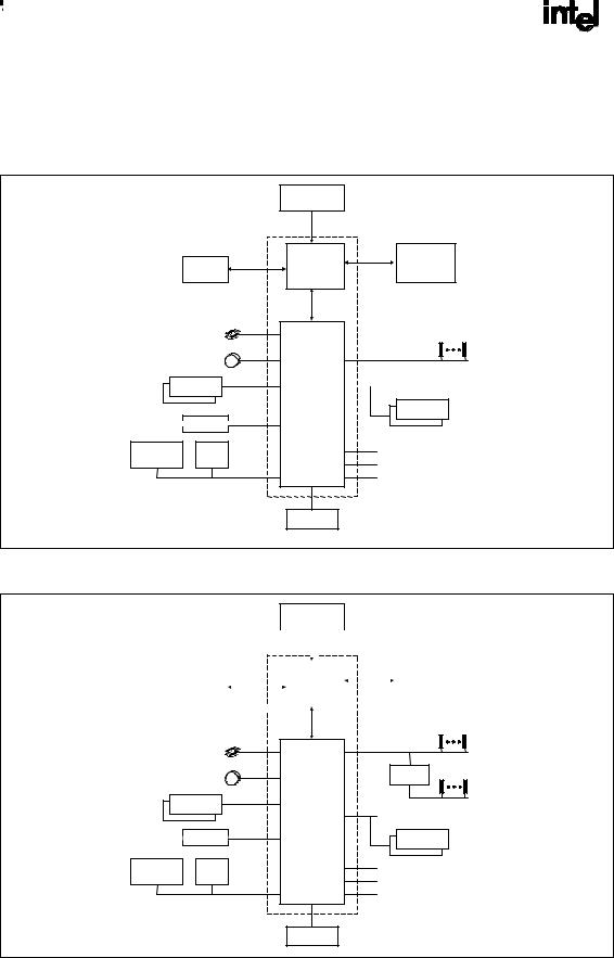
The following figures show typical platform configurations using the Intel 820E chipset:
Figure 1. Intel® 820E Chipset Platform Performance Desktop Block Diagram
|
|
|
® |
® |
|
|
|
|
Intel |
Pentium III |
|
|
|
|
Processor |
|
|
|
|
|
|
Intel® 820E Chipset |
|
|
4x AGP |
|
Intel® 82820 |
Main |
|
|
AGP 2.0 |
Controller Hub |
Memory |
||
|
Graphics |
(Direct RDRAM*) |
|||
|
|
|
(MCH) |
||
|
Controller |
|
|
|
|
|
|
|
|
|
|
|
|
|
|
Hub |
|
|
|
|
|
Interface |
|
|
4 IDE Drives |
|
|
|
PCI |
UltraATA/100/66/33 |
|
|
|
||
|
|
|
Slots |
||
|
|
|
|
|
|
4 USB Ports; 2 HC |
|
|
|
PCI Bus |
|
|
|
|
|
||
AC'97 Codec(s) |
AC'97 2.1 |
|
|
Power Management |
|
|
(optional) |
|
I/O Controller Hub |
||
|
|
|
|||
|
|
|
|
||
|
|
|
Intel® 82801BA |
Clock Generators |
|
|
|
|
|
(ICH2) |
|
|
LAN Connect |
|
|
|
|
|
|
|
|
|
|
Other ASICs |
Super I/O |
|
|
|
System Management (TCO) |
(optional) |
|
|
|
2 |
|
|
|
|
|
||
|
|
LPC I/F |
|
|
SMBus/IC |
|
|
|
|
GPIO |
|
|
|
|
|
|
|
|
|
|
FWH Flash |
|
|
|
|
|
|
BIOS |
|
|
|
|
|
|
sys_blk_820E |
Figure 2. Intel® 820E Chipset Platform Performance Desktop Block Diagram (with ISA Bridge)
Intel ® Pentium ® III
Processor
|
|
|
|
|
|
|
|
|
|
|
|
|
|
|
|
|
|
|
Intel ® 820E Chipset |
|
|||
|
|
|
|
|
|
|
|
|
|
|
|
|
|
|
|
|
Intel® 82820 Memory |
|
|
|
Main |
||
4x AGP |
|
AGP 2.0 |
Controller Hub |
|
|
|
Memory |
||||
|
|
|
|||||||||
Graphics |
|
|
(Direct RDRAM*) |
||||||||
|
|
|
|
(MCH) |
|
|
|
||||
Controller |
|
|
|
|
|
|
|||||
|
|
|
|
|
|
|
|
|
|
|
|
|
|
|
|
|
|
|
|
|
|
|
|
|
|
|
|
|
|
|
|
|
|
|
|
|
|
Hub |
|
PCI |
|
|
Interface |
|
|
|
|
|
|
Slots |
4 IDE Drives |
|
PCI Bus |
|
|
UltraATA/100/66/33 |
|
|
|
|
4 USB Ports; |
2 HC |
|
ISA Bridge |
ISA |
|
(optional) |
Slots |
||
AC'97 Codec(s) |
AC'97 2.1 |
|
|
|
|
|
|
||
(optional) |
I/O Controller Hub |
|
|
|
|
|
Power Management |
|
|
|
|
Intel® 82801BA |
|
|
|
|
|
|
|
|
|
(ICH2) |
|
|
LAN Connect |
|
Clock Generators |
|
|
Other ASICs |
Super I/O |
|
System Management (TCO) |
|
(optional) |
|
|
|
|
|
|
SMBus/I 2C |
|
|
|
|
LPC I/F |
|
|
|
|
GPIO |
|
|
|
|
|
|
|
|
|
FWH Flash |
|
|
|
|
BIOS |
sys_blk_isa_820E |
|
|
|
|
||
18 |
Design Guide |
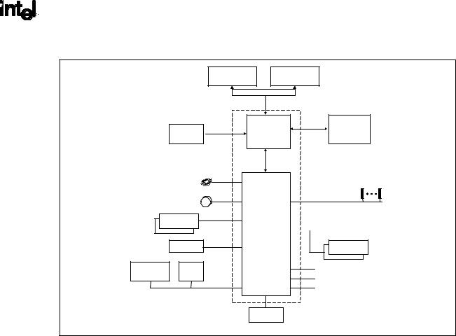
Intel® 820E Chipset
R
Figure 3. Intel® 820E Chipset Platform Dual-Processor Performance Desktop Block Diagram
Intel® Pentium® III
Processor
Intel® Pentium® III
Processor
Intel® 820E Chipset
4x AGP
Graphics  AGP 2.0
Controller
|
4 IDE Drives |
|
UltraATA/100/66/33 |
|
|
4 USB Ports; 2 HC |
|
|
AC'97 Codec(s) |
AC'97 2.1 |
|
|
(optional) |
|
|
LAN Connect |
|
Other ASICs |
Super I/O |
|
(optional) |
|
|
|
|
|
|
|
LPC I/F |
Intel® |
Main |
|
82820 Memory |
||
Memory |
||
Controller Hub |
||
(Direct RDRAM*) |
||
(MCH) |
||
|
||
Hub |
|
|
Interface |
|
|
|
PCI |
|
|
Slots |
|
|
PCI Bus |
|
I/O Controller Hub |
Power Management |
|
Intel® 82801BA |
||
|
||
(ICH2) |
|
|
|
Clock Generators |
|
|
System Management (TCO) |
|
|
SMBus/I2C |
|
|
GPIO |
|
FWH Flash |
|
|
BIOS |
|
|
|
sys_blk_2P_820E |
Design Guide |
19 |

Intel® 820E Chipset
R
1.4.Platform Initiatives
1.4.1.Direct Rambus RAM (RDRAM*)
The Direct Rambus RAM (RDRAM) initiative provides the memory bandwidth necessary to obtain optimal performance from the Pentium III processor as well as a high-performance AGP graphics controller. The MCH RDRAM interface supports 266 MHz, 300 MHz, 356 MHz, and 400 MHz operation. The latter delivers 1.6 GB/s of theoretical memory bandwidth, which is twice the memory bandwidth of 100 MHz SDRAM systems. Coupled with the greater bandwidth, the heavily pipelined RDRAM protocol provides substantially more efficient data transfer. The RDRAM memory interface can utilize more than 95% of the 1.6-GB/s theoretical maximum bandwidth.
In addition to the RDRAM’s performance features, the new memory architecture provides enhanced power management capabilities. The powerdown mode of operation allows Intel 820E chipset-based systems to provide cost-effective support of Suspend to RAM.
1.4.2.Streaming SIMD Extensions
The Pentium III processor provides 70 new streaming SIMD (single-instruction, multiple-data) extensions. The Pentium III processor’s new extensions are floating-point SIMD extensions. Intel® MMX™ technology provides integer SIMD extensions. The Pentium III processor’s new extensions complement the Intel MMX technology SIMD extensions and provide a performance boost to floating- point-intensive 3D applications.
1.4.3.AGP 2.0
In combination with Direct RDRAM memory technology, the AGP 2.0 interface allows graphics controllers to access main memory at over 1 GB/s, which is twice the AGP bandwidth of previous AGP platforms. AGP 2.0 provides the infrastructure necessary for photorealistic 3D. In conjunction with Direct RDRAM and the Pentium III processor’s new streaming SIMD extensions, AGP 2.0 delivers the next level of 3D graphics performance.
1.4.4.Hub Interface
As the I/O speed has increased, the demand placed on the PCI bus by the I/O bridge has become significant. With the addition of AC’97 and ATA/100, coupled with the existing USB, I/O requirements will begin to affect PCI bus performance. The Intel 820E chipset’s hub interface architecture ensures that the I/O subsystem both PCI and the integrated I/O features (IDE, AC’97, USB, etc.) will receive adequate bandwidth. By placing the I/O bridge on the hub interface instead of the PCI, the hub architecture ensures that both the I/O functions integrated into the ICH2 and the PCI peripherals will obtain the bandwidth necessary for peak performance. In addition, the hub interface’s lower pin count allows a smaller package for the MCH and ICH2.
20 |
Design Guide |
Intel® 820E Chipset
R
1.4.5.Integrated LAN Controller
The ICH2 component incorporates an integrated LAN Controller. Its bus master capabilities enable the component to process high-level commands and perform multiple operations, which lowers processor utilization by off-loading communication tasks from the processor.
The ICH2 functions with several options of LAN connect components, allowing the targeting of the desired market segment. The Intel® 82562EH component provides a HomePNA 1-Mbit/sec connection. The Intel® 82562ET component provides a basic Ethernet* 10/100 connection. The Intel® 82562EM component provides an Ethernet 10/100 connection with the added flexibility of Alert on LAN. More advanced LAN solutions can be implemented with the Intel® 82550 or other PCI-based product offerings.
1.4.6.Ultra ATA/100 Support
The ICH2 (82801BA) component supports the IDE controller with two sets of interface signals (primary and secondary) that can be enabled independently, tri-stated or driven low. The component supports UltraATA/100, Ultra ATA/66, UltraATA/33, and multiword p modes for transfers of up to
100Mbytes/sec.
1.4.7.Expanded USB Support
The ICH2 component contains two USB host controllers. Each host controller includes a root hub with two separate USB ports each, for a total of four USB ports. The addition of a USB host controller expands the functionality of the platform.
1.4.8.Manageability
The Intel 820E chipset platform integrates several functions designed to manage the system and lower the system’s total cost of ownership (TCO). These system management functions are designed to report errors, diagnose the system, and recover from system lock-ups, without the aid of an external microcontroller.
TCO Timer
The ICH2 integrates a programmable TCO timer, which is used to detect system locks. The first expiration of the timer generates an SMI#, which the system can use to recover from a software lock. The second expiration of the timer causes a system reset, to recover from a hardware lock.
Processor Present Indicator
The ICH2 looks for the processor to fetch the first instruction after reset. If the processor does not fetch the first instruction, the ICH2 will reboot the system at the safe-mode frequency multiplier.
ECC Error Reporting
After detecting an ECC error, the MCH can send one of several messages to the ICH2. The MCH can instruct the ICH2 to generate either an SMI#, NMI#, SERR# or TCO interrupt.
Design Guide |
21 |

Intel® 820E Chipset
R
Function Disable
The ICH2 provides the ability to disable the following functions: AC’97 Modem, AC’97 Audio, IDE, USB or SMBus. Once disabled, these functions no longer decode I/O, memory or PCI configuration space. Also, no interrupts or power management events are generated by the disabled functions.
Intruder Detect
The ICH2 provides an input signal (INTRUDER#) that can be attached to a switch that is activated when the system case is opened. The ICH2 can be programmed to generate an SMI# or TCO interrupt resulting from an active INTRUDER# signal.
SMBus
The ICH2 integrates an SMBus controller. The SMBus provides an interface to manage peripherals such as serial presence detection (SPD) on RIMMs and thermal sensors. The slave interface allows an external microcontroller to access system resources.
The Intel 820E chipset platform integrates several functions designed to expand the capability of interfacing several components to the system.
Interrupt Controller
The interrupt capabilities of the Intel 820E chipset platform expands support for up to eight PCI interrupt pins and PCI 2.2 message-based interrupts. In addition, the ICH2 supports system bus interrupt delivery.
FWH Flash BIOS
The Intel 820E chipset-based system platform supports firmware hub BIOS memory sizes up to 8 MB, for increased system flexibility.
Alert on LAN*
The ICH2 supports Alert on LAN. In response to a TCO event (intruder detect, thermal event, processor not booting), the ICH2 sends a message over ALERTCLK and ALERTDATA to alert the network manager.
22 |
Design Guide |

Intel® 820E Chipset
R
1.4.9.AC’97
The Audio Codec ’97 (AC’97) specification defines a digital interface that can be used to attach an audio codec (AC), a modem codec (MC), an audio/modem codec (AMC) or both an AC and an MC. The AC’97 specification defines the interface between the system logic and the audio or modem codec, known as the AC’97 Digital Link.
The Intel 820E chipset platform’s AC’97 (with the appropriate codecs) not only replaces ISA audio and modem functionality, but also improves overall platform integration by incorporating the AC’97 digital link. The use of the ICH2-integrated AC’97 digital link reduces cost and eases migration from ISA.
By using an audio codec, the AC’97 digital link allows for cost-effective, high-quality, integrated audio on an Intel 820E chipset-based platform. In addition, an AC’97 soft modem can be implemented with the use of a modem codec. Several system options exist when implementing AC’97. The ICH2-integrated digital link allows several external codecs to be connected to the ICH2. The system designer can provide audio with an audio codec, a modem with a modem codec, or an integrated audio/modem codec (Figure 4C). The digital link is expanded to support two audio codecs or a combination of an audio and modem codec (Figures 4A and 4B).
The modem implementations for different countries must be taken into consideration, because telephone systems may vary. By using a split design, the audio codec can be on-board and the modem codec can be placed on a riser. Intel is developing an AC’97 digital link connector. With a single integrated codec, or AMC, both audio and modem can be routed to a connector near the rear panel, where the external ports can be located.
The digital link in the ICH2 is compliant with Revision 2.1 of the AC’97 specification, so it supports two codecs with independent PCI functions for audio and modem. Microphone input and left and right audio channels are supported for a high quality, two-speaker audio solution. Wake on Ring from Suspend also is supported with the appropriate modem codec.
The ICH2 expands the audio capability with support for up to six channels of PCM audio output (full AC3 decode). Six-channel audio consists of Front Left, Front Right, Back Left, Back Right, Center, and Woofer, for a complete surround-sound effect. ICH2 has expanded support for two audio codecs on the AC’97 digital link.
Design Guide |
23 |
Intel® 820E Chipset
R
Figure 4. (A-C) AC’97 Connections
4A. AC'97 with Audio Codecs (4-Channel Secondary)
|
|
AC’97 |
|
|
Audio |
|
AC’97 Digital |
Codec |
ICH2 360 |
Link |
Audio Port |
EBGA |
|
|
|
|
|
|
|
AC’97 |
|
|
Audio |
|
|
Codec |
|
|
Audio Port |
4B. AC'97 with Modem and Audio Codecs |
Modem Port |
|
|
|
|
|
|
AC’97 |
|
|
Modem |
|
AC’97 Digital |
Codec |
ICH2 360 |
Link |
|
EBGA |
|
|
|
|
AC’97 |
|
|
Audio/ |
|
|
Codec |
|
|
Audio Port |
4C. AC'97 with Audio/Modem Codec |
Modem Port |
|
|
AC’97 Digital |
AC’97 |
ICH2 360 |
Link |
|
EBGA |
|
Audio/ |
|
Modem |
|
|
|
|
|
|
Codec |
|
|
Audio Port |
|
|
AC97_conn |
24 |
Design Guide |

Intel® 820E Chipset
R
1.4.10.Low-Pin-Count (LPC) Interface
In the Intel 820E chipset platform, the super I/O component has migrated to the Low-Pin-Count (LPC) interface. Migration to the LPC interface enables lower-cost super I/O designs. The LPC super I/O component requires the same feature set as traditional super I/O components. It should include a keyboard and mouse controller, floppy disk controller, and serial and parallel ports. In addition to the super I/O features, an integrated game port is recommended because the AC’97 interface does not provide support for a game port. In systems with ISA audio, the game port typically existed on the audio card. The fifteen-pin game port connector provides for two joysticks and a two-wire MPU-401 MIDI interface. Consult your super I/O vendor for a comprehensive list of devices offered and features supported.
In addition, depending on system requirements, a device bay controller and USB hub could be integrated into the LPC super I/O component. For systems requiring ISA support, an ISA-IRQ to serial-IRQ converter is required. This converter could be integrated into the super I/O.
Design Guide |
25 |

Intel® 820E Chipset
R
This page is intentionally left blank.
26 |
Design Guide |

Intel® 820E Chipset
R
2.Layout/Routing Guidelines
This chapter documents the motherboard layout and routing guidelines for Intel 820E chipset-based systems. This chapter does not discuss the functional aspects of any bus or the layout guidelines for an add-in device.
Caution: If the guidelines in this document are not followed, it is very important to complete thorough signal integrity and timing simulations for each design. Even if the guidelines are followed, critical signals still should be simulated to ensure proper signal integrity and flight time. As bus speeds increase, it is imperative that the guidelines documented be followed precisely. Any deviation from these guidelines must be simulated!
2.1.General Recommendations
The trace impedance typically noted (i.e., 60 Ω ± 10%) is the “nominal” trace impedance. That is, it is the impedance of a trace when not subjected to the fields created by changing the current in neighboring traces. When calculating flight times, it is important to consider the minimum and maximum impedance of a trace based on the switching of neighboring traces. This trace-to-trace coupling can be minimized by using wider spaces between the traces. In addition, these wider spaces reduce crosstalk and settling time.
Coupling between two traces is a function of the coupled length, the distance separating the traces, the signal edge rate, and the degree of mutual capacitance and inductance. To minimize the effects of trace- to-trace coupling, the routing guidelines documented in this chapter should be followed. In addition, the PCB should be fabricated as documented in Section 5.1.
Except where noted, all recommendations in this chapter assume 5 mil-wide traces. If the trace width is greater than 5 mils, then the trace spacing requirements must be adjusted accordingly (and linearly). For example, this chapter recommends routing most AGP signals with 5 mil traces on 20 mil spaces (1:4). If 6 mil traces are used, then 24 mil spaces must be used (also 1:4). Using a wider trace—and therefore wider spaces—will make routing more difficult.
Additionally, these routing guidelines are created using the stack-up described in Section 5.1. If this stack-up is not used, extremely thorough simulations of every interface must be completed. Using a thicker dielectric (prepreg) will make routing very difficult or impossible.
2.2.Component Quadrant Layout
The quadrant layouts shown are approximate and the exact ball assignments should be used to conduct routing analysis. These quadrant layouts are designed for use during component placement.
Design Guide |
27 |
Intel® 820E Chipset
Figure 5. MCH 324-Ball µBGA* CSP Quadrant Layout (Top View)
Pin 1
System bus
AGP 2.0 |
MCH |
|
|
||
interfaceHub |
(324-Ball |
|
µBGA* CSP) |
||
|
Direct RDRAM*
R
System bus
mch_quad
Figure 6. ICH2 360-Ball EBGA Quadrant Layout (Top View)
Hub interface |
Processor |
|
|
|
IDE |
LAN |
|
|
|
ICH2 |
|
|
360-Ball |
|
|
EBGA |
|
|
|
SM bus |
|
|
AC'97 |
PCI |
LPC |
USB |
|
|
quad_ICH2 |
28 |
Design Guide |
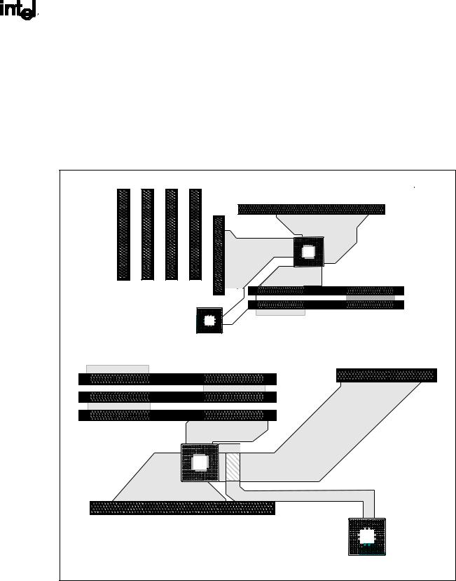
Intel® 820E Chipset
R
2.3.Intel® 820E Chipset Component Placement
Notes:
1.The ATX and NLX placements and layouts shown in the following figure are recommended for single (UP) Intel 820E chipset-based system design.
2.The trace length limitation between critical connections will be discussed later in this document.
3.The figure is for reference only.
Figure 7. Sample ATX and NLX MCH/ICH2 Component Placement
a. Sample ATX MCH/ICH2 Component Placement |
|
|
CPU Host |
|
Bus |
AGP |
MCH |
|
|
2.0 |
|
Hub |
Direct |
Interface |
|
|
RDRAM |
RDRAM Termination |
|
ICH2 |
|
b. Sample NLX MCH/ICH2 Component Placement |
atx_mch-ich2_place |
|
|
RDRAM* Termination |
|
Direct RDRAM |
AGP 2.0 |
|
|
MCH |
|
CPU Host Bus |
Hub Link |
|
|
|
ICH2 |
|
nlx_mch-ich2_place |
Note: Actual ICH2 placement may vary.
Design Guide |
29 |

Intel® 820E Chipset
R
2.4.Core Chipset Routing Recommendations
The following two figures show MCH core routing examples:
Figure 8. Primary-Side MCH Core Routing Example (ATX)
30 |
Design Guide |
Loading...