


 Loading...
Intel CORE I7-620 UE, CORE I7-620LE, CELERON PROCESSOR U3405, CORE I7-610E, CORE I7-660UE Manual
...Intel® CoreTM i7-660UE, i7-620LE/
UE, i7-610E, i5-520E, i3-330E and
Intel® Celeron® Processor P4505,
U3405 Series
Datasheet Addendum
August 2010
Document Number: 323178-003

INFORMATION IN THIS DOCUMENT IS PROVIDED IN CONNECTION WITH INTEL® PRODUCTS. NO LICENSE, EXPRESS OR IMPLIED, BY ESTOPPEL OR OTHERWISE, TO ANY INTELLECTUAL PROPERTY RIGHTS IS GRANTED BY THIS DOCUMENT. EXCEPT AS PROVIDED IN INTEL'S TERMS AND CONDITIONS OF SALE FOR SUCH PRODUCTS, INTEL ASSUMES NO LIABILITY WHATSOEVER, AND INTEL DISCLAIMS ANY EXPRESS OR IMPLIED WARRANTY, RELATING TO SALE AND/OR USE OF INTEL PRODUCTS INCLUDING LIABILITY OR WARRANTIES RELATING TO FITNESS FOR A PARTICULAR PURPOSE, MERCHANTABILITY, OR INFRINGEMENT OF ANY PATENT, COPYRIGHT OR OTHER INTELLECTUAL PROPERTY RIGHT. Intel products are not intended for use in medical, life saving, life sustaining, critical control or safety systems, or in nuclear facility applications.
Intel may make changes to specifications and product descriptions at any time, without notice.
Intel Corporation may have patents or pending patent applications, trademarks, copyrights, or other intellectual property rights that relate to the presented subject matter. The furnishing of documents and other materials and information does not provide any license, express or implied, by estoppel or otherwise, to any such patents, trademarks, copyrights, or other intellectual property rights.
Designers must not rely on the absence or characteristics of any features or instructions marked “reserved” or “undefined.” Intel reserves these for future definition and shall have no responsibility whatsoever for conflicts or incompatibilities arising from future changes to them.
Intel processor numbers are not a measure of performance. Processor numbers differentiate features within each processor family, not across different processor families. See http://www.intel.com/products/processor_number for details.
The Intel® CoreTM i7-620LE/UE, i7-610E and i5-520E Processor Series may contain design defects or errors known as errata which may cause the product to deviate from published specifications. Current characterized errata are available on request.
Hyper-Threading Technology requires a computer system with an Intel® Pentium® 4 processor supporting HT Technology and a HT Technology enabled chipset, BIOS and operating system. Performance will vary depending on the specific hardware and software you use. See http://www.intel.com/ products/ht/Hyperthreading_more.htm for additional information.
Contact your local Intel sales office or your distributor to obtain the latest specifications and before placing your product order.
Copies of documents which have an order number and are referenced in this document, or other Intel literature may be obtained by calling 1-800-548-4725 or by visiting Intel's website at http://www.intel.com.
BunnyPeople, Celeron, Celeron Inside, Centrino, Centrino logo, Core Inside, Dialogic, FlashFile, i960, InstantIP, Intel, Intel logo, Intel386, Intel486, Intel740, IntelDX2, IntelDX4, IntelSX2, Intel Core, Intel Inside, Intel Inside logo, Intel. Leap ahead., Intel. Leap ahead. logo, Intel NetBurst, Intel NetMerge, Intel NetStructure, Intel SingleDriver, Intel SpeedStep, Intel StrataFlash, Intel Viiv, Intel vPro, Intel XScale, IPLink, Itanium, Itanium Inside, MCS, MMX, Oplus, OverDrive, PDCharm, Pentium, Pentium Inside, skoool, Sound Mark, The Journey Inside, VTune, Xeon, and Xeon Inside are trademarks or registered trademarks of Intel Corporation or its subsidiaries in the United States and other countries.
*Other names and brands may be claimed as the property of others. Copyright © 2010, Intel Corporation. All Rights Reserved.
Intel® CoreTM i7-660UE, i7-620LE/UE, i7-610E, i5-520E, i3-330E and Intel® Celeron® Processor |
P4505, U3405 Series |
Datasheet Addendum |
August 2010 |
2 |
Document Number: 323178-003 |

Contents
1 |
Introduction and Features Summary ......................................................................... |
8 |
||
|
1.1 |
Introduction ....................................................................................................... |
8 |
|
|
1.2 |
Interfaces ........................................................................................................ |
10 |
|
|
|
1.2.1 |
System Memory Support ......................................................................... |
10 |
|
|
1.2.2 |
PCI Express* ......................................................................................... |
10 |
|
1.3 |
Package ........................................................................................................... |
11 |
|
|
1.4 |
Terminology ..................................................................................................... |
12 |
|
|
1.5 |
Related Documents ........................................................................................... |
13 |
|
2 |
Interfaces................................................................................................................ |
|
15 |
|
|
2.1 |
System Memory Interface .................................................................................. |
15 |
|
|
|
2.1.1 System Memory Technology Supported ..................................................... |
15 |
|
|
|
2.1.2 System Memory Timing Support............................................................... |
16 |
|
|
|
2.1.3 System Memory Organization Modes......................................................... |
16 |
|
|
|
2.1.4 Rules for Populating Memory Slots............................................................ |
18 |
|
|
|
2.1.5 Technology Enhancements of Intel® Fast Memory Access (Intel® FMA).......... |
18 |
|
|
|
2.1.6 |
DRAM Clock Generation........................................................................... |
19 |
|
|
2.1.7 |
DDR3 On-Die Termination ....................................................................... |
19 |
|
2.2 |
PCI Express* Interface....................................................................................... |
19 |
|
|
|
2.2.1 PCI Express* Configuration Mechanism ..................................................... |
19 |
|
|
|
2.2.2 PCI Express Port Bifurcation..................................................................... |
20 |
|
3 |
Signal Description ................................................................................................... |
21 |
||
|
3.1 |
System Memory Interface .................................................................................. |
21 |
|
|
3.2 |
Reset and Miscellaneous Signals.......................................................................... |
24 |
|
4 |
Electrical Specifications........................................................................................... |
25 |
||
|
4.1 |
Signal Groups ................................................................................................... |
25 |
|
|
4.2 |
DC Specifications .............................................................................................. |
25 |
|
|
|
4.2.1 Voltage and Current Specifications............................................................ |
25 |
|
5 |
Processor Ball and Signal Information..................................................................... |
27 |
||
|
5.1 |
Processor Ball Assignments................................................................................. |
27 |
|
6 |
Processor Configuration Registers........................................................................... |
70 |
||
|
6.1 |
Register Terminology ......................................................................................... |
70 |
|
|
|
6.1.1 |
DEVEN - Device Enable ........................................................................... |
72 |
|
|
6.1.2 |
ERRSTS - Error Status ............................................................................ |
73 |
|
|
6.1.3 |
ERRCMD - Error Command ...................................................................... |
74 |
|
|
6.1.4 |
SMICMD - SMI Command ........................................................................ |
76 |
|
|
6.1.5 C0WRDATACTRL - Channel 0 Write Data Control......................................... |
77 |
|
|
|
6.1.6 COECCERRLOG - Channel 0 ECC Error Log ................................................. |
78 |
|
|
|
6.1.7 C1WRDATACTRL - Channel 1 Write Data Control......................................... |
80 |
|
|
|
6.1.8 C1ECCERRLOG - Channel 1 ECC Error Log ................................................. |
80 |
|
|
6.2 |
PCI Device 6..................................................................................................... |
81 |
|
|
|
6.2.1 |
VID6 - Vendor Identification .................................................................... |
85 |
|
|
6.2.2 |
DID6 - Device Identification..................................................................... |
85 |
|
|
6.2.3 |
PCICMD6 - PCI Command........................................................................ |
86 |
|
|
6.2.4 |
PCISTS6 - PCI Status.............................................................................. |
88 |
|
|
6.2.5 |
RID6 - Revision Identification................................................................... |
90 |
|
|
6.2.6 |
CC6 - Class Code ................................................................................... |
90 |
|
|
6.2.7 |
CL6 - Cache Line Size ............................................................................. |
91 |
|
|
6.2.8 |
HDR6 - Header Type............................................................................... |
91 |
|
|
6.2.9 |
PBUSN6 - Primary Bus Number ................................................................ |
92 |
Intel® CoreTM i7-660UE, i7-620LE/UE, i7-610E, i5-520E, i3-330E and Intel® Celeron® Processor |
P4505, U3405 Series |
August 2010 |
Datasheet Addendum |
Document Number: 323178-003 |
3 |

6.2.10 |
SBUSN6 - Secondary Bus Number............................................................. |
92 |
6.2.11 |
SUBUSN6 - Subordinate Bus Number ........................................................ |
93 |
6.2.12 |
IOBASE6 - I/O Base Address .................................................................... |
93 |
6.2.13 |
IOLIMIT6 - I/O Limit Address ................................................................... |
94 |
6.2.14 |
SSTS6 - Secondary Status ....................................................................... |
95 |
6.2.15 |
MBASE6 - Memory Base Address............................................................... |
96 |
6.2.16 |
MLIMIT6 - Memory Limit Address.............................................................. |
97 |
6.2.17 |
PMBASE6 - Prefetchable Memory Base Address........................................... |
98 |
6.2.18 |
PMLIMIT6 - Prefetchable Memory Limit Address .......................................... |
99 |
6.2.19 |
PMBASEU6 - Prefetchable Memory Base Address Upper.............................. |
100 |
6.2.20 |
PMLIMITU6 - Prefetchable Memory Limit Address Upper ............................. |
101 |
6.2.21 |
CAPPTR6 - Capabilities Pointer................................................................ |
102 |
6.2.22 |
INTRLINE6 - Interrupt Line .................................................................... |
102 |
6.2.23 |
INTRPIN6 - Interrupt Pin........................................................................ |
103 |
6.2.24 |
BCTRL6 - Bridge Control ........................................................................ |
103 |
6.2.25 |
PM_CAPID6 - Power Management Capabilities .......................................... |
105 |
6.2.26 |
PM_CS6 - Power Management Control/Status ........................................... |
106 |
6.2.27 |
SS_CAPID - Subsystem ID and Vendor ID Capabilities ............................... |
108 |
6.2.28 |
SS - Subsystem ID and Subsystem Vendor ID .......................................... |
108 |
6.2.29 |
MSI_CAPID - Message Signaled Interrupts Capability ID ............................ |
109 |
6.2.30 |
MC - Message Control............................................................................ |
109 |
6.2.31 |
MA - Message Address........................................................................... |
111 |
6.2.32 |
MD - Message Data............................................................................... |
111 |
6.2.33 |
PEG_CAPL - PCI Express-G Capability List ................................................ |
112 |
6.2.34 |
PEG_CAP - PCI Express-G Capabilities ..................................................... |
112 |
6.2.35 |
DCAP - Device Capabilities ..................................................................... |
113 |
6.2.36 |
DCTL - Device Control ........................................................................... |
114 |
6.2.37 |
DSTS - Device Status ............................................................................ |
115 |
6.2.38 |
LCAP - Link Capabilities ......................................................................... |
116 |
6.2.39 |
LCTL - Link Control ............................................................................... |
119 |
6.2.40 |
LSTS - Link Status ................................................................................ |
121 |
6.2.41 |
SLOTCAP - Slot Capabilities.................................................................... |
123 |
6.2.42 |
SLOTCTL - Slot Control.......................................................................... |
124 |
6.2.43 |
SLOTSTS - Slot Status........................................................................... |
127 |
6.2.44 |
RCTL - Root Control .............................................................................. |
129 |
6.2.45 |
RSTS - Root Status ............................................................................... |
130 |
6.2.46 |
LCTL2 - Link Control 2........................................................................... |
130 |
6.2.47 |
LSTS2 - Link Status 2............................................................................ |
132 |
6.2.48 |
PEGLC - PCI Express-G Legacy Control .................................................... |
133 |
6.3 PCI Device 6 - Extended Configuration................................................................ |
134 |
|
6.3.1 |
VCECH - Virtual Channel Enhanced Capability Header ................................ |
134 |
6.3.2 |
PVCCAP1 - Port VC Capability Register 1 .................................................. |
134 |
6.3.3 |
PVCCAP2 - Port VC Capability Register 2 .................................................. |
135 |
6.3.4 |
PVCCTL - Port VC Control....................................................................... |
136 |
6.3.5 |
VC0RCAP - VC0 Resource Capability ........................................................ |
136 |
6.3.6 |
VC0RCTL - VC0 Resource Control ............................................................ |
137 |
6.3.7 |
VC0RSTS - VC0 Resource Status............................................................. |
138 |
Intel® CoreTM i7-660UE, i7-620LE/UE, i7-610E, i5-520E, i3-330E and Intel® Celeron® Processor |
P4505, U3405 Series |
Datasheet Addendum |
August 2010 |
4 |
Document Number: 323178-003 |

Figures
1Intel® CoreTM i7-660UE, i7-620LE/UE, i7-610E, i5-520E, i3-330E and Intel® Celeron®
®CoreTM i7 processor based
|
low-power platform .................................................................................................... |
9 |
2 |
Intel® Flex Memory Technology Operation................................................................... |
17 |
3 |
Dual-Channel Symmetric (Interleaved) and Dual-Channel Asymmetric Modes .................. |
18 |
4 |
PCI Express* Related Register Structures in the Intel® CoreTM i7-660UE, i7-620LE/UE, |
|
|
i7-610E, i5-520E, i3-330E and Intel® Celeron® Processor P4505, U3405 Series ............... |
20 |
5 |
Intel® CoreTM i7-660UE, i7-620LE/UE, i7-610E, i5-520E, i3-330E and Intel® Celeron® |
|
|
Processor P4505, U3405 Series Ballmap (Top View, Upper-Left Quadrant) ....................... |
28 |
6 |
Intel® CoreTM i7-660UE, i7-620LE/UE, i7-610E, i5-520E, i3-330E and Intel® Celeron® |
|
|
Processor P4505, U3405 Series Ballmap (Top View, Upper-Right Quadrant) ..................... |
29 |
7 |
Intel® CoreTM i7-660UE, i7-620LE/UE, i7-610E, i5-520E, i3-330E and Intel® Celeron® |
|
|
Processor P4505, U3405 Series Ballmap (Top View, Lower-Left Quadrant) ....................... |
30 |
8 |
Intel® CoreTM i7-660UE, i7-620LE/UE, i7-610E, i5-520E, i3-330E and Intel® Celeron® |
|
|
Processor P4505, U3405 Series Ballmap (Top View, Lower-Right Quadrant) ..................... |
31 |
Tables |
|
|
1 |
Processor Documents ............................................................................................... |
13 |
2 |
PCH Documents ....................................................................................................... |
14 |
3 |
Public Specifications ................................................................................................. |
14 |
4 |
Supported DIMM Module Configurations ...................................................................... |
15 |
5 |
DDR3 System Memory Timing Support........................................................................ |
16 |
6 |
Signal Description Buffer Types.................................................................................. |
21 |
7 |
Memory Channel A ................................................................................................... |
21 |
8 |
Memory Channel B ................................................................................................... |
23 |
9 |
Reset and Miscellaneous Signals ................................................................................ |
24 |
10 |
Mobile Signal Groups1 .............................................................................................. |
25 |
11 |
DDR3 Signal Group DC Specifications ......................................................................... |
25 |
12 |
Intel® CoreTM i7-660UE, i7-620LE/UE, i7-610E, i5-520E, i3-330E and Intel® Celeron® |
|
|
Processor P4505, U3405 Series Ball List by Ball Name................................................... |
32 |
13 |
Intel® CoreTM i7-660UE, i7-620LE/UE, i7-610E, i5-520E, i3-330E and Intel® Celeron® |
|
|
Processor P4505, U3405 Series Ball List by Ball Number................................................ |
49 |
14 |
Register Terminology................................................................................................ |
70 |
15 |
DEVEN - Device Enable Register................................................................................. |
72 |
16 |
Error Status Register ................................................................................................ |
73 |
17 |
Error Command Registers ......................................................................................... |
75 |
18 |
SMI Command Registers ........................................................................................... |
76 |
19 |
Channel 0 Write Data Control Registers....................................................................... |
77 |
20 |
Channel 0 ECC Error Registers ................................................................................... |
78 |
21 |
Channel 1 Write Data Control Registers....................................................................... |
80 |
22 |
Channel 1 ECC Error Registers ................................................................................... |
81 |
23 |
PCI Device 6 Register ............................................................................................... |
82 |
24 |
VID6 - Vendor Identification Register.......................................................................... |
85 |
25 |
DID6 - Device Identification Register .......................................................................... |
85 |
26 |
PCICMD6 - PCI Command Register ............................................................................. |
86 |
27 |
PCISTS6 - PCI Status Register ................................................................................... |
88 |
28 |
RID6 - Revision Identification Register ........................................................................ |
90 |
29 |
CC6 - Class Code Register ......................................................................................... |
90 |
30 |
CL6 - Cache Line Size Register................................................................................... |
91 |
31 |
HDR6 - Header Type Register .................................................................................... |
91 |
32 |
PBUSN6 - Primary Bus Number Register...................................................................... |
92 |
33 |
SBUSN6 - Secondary Bus Number Register.................................................................. |
92 |
34 |
SUBUSN6 - Subordinate Bus Number Register ............................................................. |
93 |
35 |
IOBASE6 - I/O Base Address Register ......................................................................... |
94 |
Intel® CoreTM i7-660UE, i7-620LE/UE, i7-610E, i5-520E, i3-330E and Intel® Celeron® Processor |
P4505, U3405 Series |
August 2010 |
Datasheet Addendum |
Document Number: 323178-003 |
5 |

36 |
IOLIMIT6 - I/O Limit Address Register......................................................................... |
94 |
37 |
SSTS6 - Secondary Status Register............................................................................. |
95 |
38 |
MBASE6 - Memory Base Address Register .................................................................... |
96 |
39 |
MLIMIT6 - Memory Limit Address Register ................................................................... |
97 |
40 |
PMBASE6 - Prefetchable Memory Base Address Register ................................................ |
98 |
41 |
PMLIMIT6 - Prefetchable Memory Limit Address Register................................................ |
99 |
42 |
PMBASEU6 - Prefetchable Memory Base Address Upper Register ................................... |
100 |
43 |
PMLIMITU6 - Prefetchable Memory Limit Address Upper Register .................................. |
101 |
44 |
CAPPTR6 - Capabilities Pointer Register ..................................................................... |
102 |
45 |
INTRLINE6 - Interrupt Line Register.......................................................................... |
102 |
46 |
INTRPIN6 - Interrupt Pin Register ............................................................................. |
103 |
47 |
BCTRL6 - Bridge Control Register ............................................................................. |
103 |
48 |
PM_CAPID6 - Power Management Capabilities Register................................................ |
105 |
49 |
PM_CS6 - Power Management Control/Status Register ................................................ |
106 |
50 |
SS_CAPID - Subsystem ID and Vendor ID Capabilities Register .................................... |
108 |
51 |
SS - Subsystem ID and Subsystem Vendor ID Register................................................ |
108 |
52 |
MSI_CAPID - Message Signaled Interrupts Capability ID Register.................................. |
109 |
53 |
MC - Message Control Register ................................................................................. |
109 |
54 |
MA - Message Address Register ................................................................................ |
111 |
55 |
MD - Message Data Register .................................................................................... |
111 |
56 |
PEG_CAPL - PCI Express-G Capability List Register...................................................... |
112 |
57 |
PEG_CAP - PCI Express-G Capabilities Register........................................................... |
112 |
58 |
DCAP - Device Capabilities Register .......................................................................... |
113 |
59 |
DCTL - Device Control Register................................................................................. |
114 |
60 |
DSTS - Device Status Register ................................................................................. |
115 |
61 |
LCAP - Link Capabilities Register............................................................................... |
116 |
62 |
LCTL - Link Control Register..................................................................................... |
119 |
63 |
LSTS - Link Status Register...................................................................................... |
121 |
64 |
SLOTCAP - Slot Capabilities Register ......................................................................... |
123 |
65 |
SLOTCTL - Slot Control Register ............................................................................... |
124 |
66 |
SLOTSTS - Slot Status Register ................................................................................ |
127 |
67 |
RCTL - Root Control Register.................................................................................... |
129 |
68 |
RSTS - Root Status Register .................................................................................... |
130 |
69 |
LCTL2 - Link Control 2 Register ................................................................................ |
130 |
70 |
LSTS2 - Link Status 2 Register ................................................................................. |
132 |
71 |
PEGLC - PCI Express-G Legacy Control Register.......................................................... |
133 |
72 |
PCI Device 6 - Extended Configuration ...................................................................... |
134 |
73 |
VCECH - Virtual Channel Enhanced Capability Header.................................................. |
134 |
74 |
PVCCAP1 - Port VC Capability Register 1.................................................................... |
135 |
75 |
PVCCAP2 - Port VC Capability Register 2.................................................................... |
136 |
76 |
PVCCTL - Port VC Control ........................................................................................ |
136 |
77 |
VC0RCAP - VC0 Resource Capability.......................................................................... |
136 |
78 |
VC0RCTL - VC0 Resource Control.............................................................................. |
138 |
79 |
VC0RSTS - VC0 Resource Status .............................................................................. |
139 |
Intel® CoreTM i7-660UE, i7-620LE/UE, i7-610E, i5-520E, i3-330E and Intel® Celeron® Processor |
P4505, U3405 Series |
Datasheet Addendum |
August 2010 |
6 |
Document Number: 323178-003 |

Revision History
Date |
Revision |
Description |
|
|
|
|
|
January 2010 |
001 |
• Initial release of this document. |
|
|
|
|
|
|
|
• Added information for the Intel® Celeron® Processor P4500 and P4505 Series. |
|
April 2010 |
002 |
• Corrected first bullet in Section 2.1.1 to “No support for mixed ECC and non-ECC DIMM |
|
|
|
configurations.” |
|
|
|
|
|
|
|
• Added information for the Intel® CoreTM i7-660UE, i3-330E and Celeron® Processor U3405 |
|
August 2010 |
003 |
• Removed all references to Celeron® Processor P4500 since it is a PGA package and does not |
|
relate to this document (was included by error in last revision). |
|||
|
|
||
|
|
• CMD mode for DDR3 is restated to 1n instead of 1n and 2n |
|
|
|
|
Intel® CoreTM i7-660UE, i7-620LE/UE, i7-610E, i5-520E, i3-330E and Intel® Celeron® Processor |
P4505, U3405 Series |
August 2010 |
Datasheet Addendum |
Document Number: 323178-003 |
7 |

Introduction and Features Summary
1Introduction and Features Summary
1.1Introduction
This Datasheet Addendum is a supplement to the Intel® CoreTM i7-600, i5-500 and i3300 Mobile Processor Series Datasheet. It contains the additional DC and AC electrical specifications, signal integrity, differential signaling specifications, pinout and signal definitions, interface functional descriptions, additional feature information and configuration registers pertinent to the implementation and operation of the Intel® CoreTM i7-660UE, i7-620LE/UE, i7-610E, i5-520E, i3-330E and Intel® Celeron® Processor P4505, U3405 Series on its respective platform.
Intel® CoreTM i7-660UE, i7-620LE/UE, i7-610E, i5-520E, i3-330E and Intel® Celeron® Processor P4505, U3405 Series is the next generation of 64-bit, multi-core mobile processor built on a 32nanometer process technology. Throughout this document, Intel® CoreTM i7-660UE, i7-620LE/UE, i7-610E, i5-520E, i3-330E and Intel® Celeron® Processor P4505, U3405 Series may be referred to as simply the processor. The processor is designed for a two-chip platform as opposed to the traditional three-chip platforms (processor, GMCH, and ICH). The two-chip platform consists of a processor and the Platform Controller Hub (PCH) and enables higher performance, lower cost, easier validation, and improved x-y footprint. The PCH may also be referred to as Mobile Intel® 5 Series Chipset (formerly Ibex Peak-M). Intel® CoreTM i7-660UE, i7620LE/UE, i7-610E, i5-520E, i3-330E and Intel® Celeron® Processor P4505, U3405 Series is designed for the Intel® CoreTM i7 processor based low-power platform and is offered in a BGA1288 package.
Included in this family of processors is an integrated graphics and memory controller die on the same package as the processor core die. This two-chip solution of a processor core die with an integrated graphics and memory controller die is known as a multi-chip package (MCP) processor.
Note: Integrated graphics and memory controller die is built on 45-nanometer process technology.
Intel® CoreTM i7-660UE, i7-620LE/UE, i7-610E, i5-520E, i3-330E and Intel® Celeron® Processor P4505, U3405 Series
Datasheet Addendum |
August 2010 |
8 |
Document Number: 323178-003 |

Introduction and Features Summary
Figure 1. |
Intel® CoreTM i7-660UE, i7-620LE/UE, i7-610E, i5-520E, i3-330E and Intel® |
||||||
|
Celeron® Processor P4505, U3405 Series on the Intel® CoreTM i7 processor |
||||||
|
based low-power platform |
|
|
|
|
||
|
|
|
|
Dual-core |
|
|
|
|
|
|
|
Processor |
|
|
|
Discrete Graphics |
Intel CoreTM i7/i5/i3 and Celeron |
|
|
||||
|
(PEG) |
PCI Express* x16 |
|
Processor |
800/1066 MT/s |
|
|
|
OR |
|
(MCP Processor) |
2 Channels |
|
||
|
Embedded |
|
|
|
|
||
|
|
GPU, Memory |
1 DIMM / Channel |
|
|||
DisplayPort* (eDP) |
|
|
|
||||
|
|
|
|
Controller |
|
|
|
|
|
|
|
|
|
DDR3 DIMMs |
|
|
|
PCI Express x 1 |
|
|
|
|
|
|
|
|
Intel® |
Flexible |
DMI2 |
|
|
|
|
|
Display Interface |
(x4) |
|
|
|
|
|
Digital Display x 3 |
|
|
|
Serial ATA |
6 Ports |
|
|
|
|
Intel® |
3 Gb/s |
||
|
|
|
|
|
|
||
|
|
|
|
|
|
|
|
|
|
LVDS Flat Panel |
|
|
Management |
USB 2.0 |
14 Ports |
|
|
|
|
Engine |
|||
|
|
|
|
|
|
||
|
|
Analog CRT |
Mobile Intel 5 Series Chipset |
|
|
||
|
|
|
|
PCH |
|
|
|
|
|
|
|
|
|
Intel® HD Audio |
|
|
|
|
|
|
|
SMBUS 2.0 |
|
|
|
SPI Flash |
SPI |
|
|
Controller Link 1 |
|
|
|
|
|
|
|
|
|
|
|
PCI |
PCI |
PCI Express* |
|
|
|
|
|
|
|
|
|
|
|
|
|
FWH |
|
|
|
Gigabit |
|
|
|
|
|
|
Network Connection |
||
|
|
|
|
|
|
||
|
|
TPM 1.2 |
|
8 PCI Express* x1 |
|
|
|
|
|
LPC |
Ports |
|
|
||
|
|
|
|
|
|||
|
|
|
(2.5 GT/s) |
|
|
||
|
|
Super I/O |
|
|
|
||
|
|
|
|
|
|
|
|
|
|
|
PECI |
|
|
|
|
|
|
|
GPIO |
|
|
|
|
Intel® CoreTM i7-660UE, i7-620LE/UE, i7-610E, i5-520E, i3-330E and Intel® Celeron® Processor P4505, U3405 Series |
|
||||||
August 2010 |
|
|
|
|
|
Datasheet Addendum |
|
Document Number: 323178-003 |
|
|
|
|
9 |
||

Introduction and Features Summary
1.2Interfaces
1.2.1System Memory Support
•One or two channels of DDR3 memory with a maximum of one DIMM per channel
•Singleand dual-channel memory organization modes
•Data burst length of eight for all memory organization modes
•Memory DDR3 data transfer rates of 800 and 1066 MT/s
•64-bit wide channels (72-bit wide including ECC)
•DDR3 I/O Voltage of 1.5 V
•Supports ECC and non-ECC, unbuffered DDR3 DIMMs
—Mixing of ECC and Non-ECC DIMMS is not supported
•Theoretical maximum memory bandwidth of:
—12.8 GB/s in dual-channel mode assuming DDR3 800 MT/s
—17.1 GB/s in dual-channel mode assuming DDR3 1066 MT/s
•1-Gb, and 2-Gb DDR3 DRAM technologies for x8 and x16 devices
•Using 2-Gb device technologies, the largest memory capacity possible is 8 GB, assuming dual-channel mode with two x8, dual-rank, un-buffered, DIMM memory configuration.
•Up to 32 simultaneous open pages, 16 per channel (assuming 4 Ranks of 8 Bank Devices)
•Memory organizations:
—Single-channel modes
—Dual-channel modes
Dual-channel symmetric (Interleaved)
Dual-channel asymmetric Intel® Flex Memory Technology
•Command launch mode of 1n
•Partial Writes to memory using Data Mask (DM) signals
•On-Die Termination (ODT)
•Intel® Fast Memory Access (Intel® FMA):
—Just-in-Time Command Scheduling
—Command Overlap
—Out-of-Order Scheduling
1.2.2PCI Express*
•The processor PCI Express* port(s) are fully-compliant to the PCI Express Base Specification, Revision 2.0 at 2.5GT/s.
•The processor supports:
—One 16-lane PCI Express port for graphics or I/O.
—Two 8-lane PCI Express ports for graphics or I/O.
•PCI Express Port 0 is mapped to PCI Device 1.
•PCI Express Port 1 is mapped to PCI Device 6.
Intel® CoreTM i7-660UE, i7-620LE/UE, i7-610E, i5-520E, i3-330E and Intel® Celeron® Processor P4505, U3405 Series
Datasheet Addendum |
August 2010 |
10 |
Document Number: 323178-003 |
Introduction and Features Summary
1.3Package
The Intel Core i7-660UE, i7-620LE/UE, i7-610E, i5-520E, i3-330E and Intel Celeron Processor P4505, U3405 Series are available on a 34 x 28 mm BGA package (BGA1288).
Note: Although the BGA1288 package is shared with Intel® CoreTM i7-640UM/LM, i7-620M/ UM/LM, i5-540M, i5-520M/UM and i5-430M Processor Series they are not ball-out compatible.
Intel® CoreTM i7-660UE, i7-620LE/UE, i7-610E, i5-520E, i3-330E and Intel® Celeron® Processor P4505, U3405 Series
August 2010 |
Datasheet Addendum |
Document Number: 323178-003 |
11 |

Introduction and Features Summary
1.4Terminology
Term |
Description |
|
|
|
|
BLT |
Block Level Transfer |
|
|
|
|
CRT |
Cathode Ray Tube |
|
|
|
|
DDR3 |
Third generation Double Data Rate SDRAM memory technology |
|
|
|
|
DP |
DisplayPort* |
|
|
|
|
DMA |
Direct Memory Access |
|
|
|
|
DMI |
Direct Media Interface |
|
|
|
|
DTS |
Digital Thermal Sensor |
|
|
|
|
ECC |
Error Correction Code |
|
|
|
|
eDP* |
Embedded DisplayPort* |
|
|
|
|
Intel® DPST |
Intel® Display Power Saving Technology |
|
Enhanced Intel |
Technology that provides power management capabilities to laptops. |
|
SpeedStep® Technology |
||
|
The Execute Disable bit allows memory to be marked as executable or non- |
|
|
executable, when combined with a supporting operating system. If code |
|
|
attempts to run in non-executable memory the processor raises an error to the |
|
Execute Disable Bit |
operating system. This feature can prevent some classes of viruses or worms |
|
|
that exploit buffer overrun vulnerabilities and can thus help improve the overall |
|
|
security of the system. See the Intel® 64 and IA-32 Architectures Software |
|
|
Developer's Manuals for more detailed information. |
|
|
|
|
EU |
Execution Unit |
|
|
|
|
(G)MCH |
Legacy component - Graphics Memory Controller Hub. |
|
|
|
|
GPU |
Graphics Processing Unit |
|
|
|
|
|
The legacy I/O Controller Hub component that contains the main PCI interface, |
|
ICH |
LPC interface, USB2, Serial ATA, and other I/O functions. It communicates with |
|
|
the legacy (G)MCH over a proprietary interconnect called DMI. |
|
|
|
|
IMC |
Integrated Memory Controller |
|
|
|
|
Intel® 64 Technology |
64-bit memory extensions to the IA-32 architecture. |
|
Intel® FDI |
Intel® Flexible Display Interface. |
|
Intel® TXT |
Intel® Trusted Execution Technology |
|
Intel® Virtualization |
Processor virtualization which when used in conjunction with Virtual Machine |
|
Technology |
Monitor software enables multiple, robust independent software environments |
|
inside a single platform. |
||
|
||
|
|
|
ITPM |
Integrated Trusted Platform Module |
|
|
|
|
IOV |
I/O Virtualization |
|
|
|
|
LCD |
Liquid Crystal Display |
|
|
|
|
|
Low Voltage Differential Signaling |
|
LVDS |
A high speed, low power data transmission standard used for display connections |
|
|
to LCD panels. |
|
|
|
|
MCP |
Multi-Chip Package |
|
|
|
|
|
Non-Critical to Function: NCTF locations are typically redundant ground or non- |
|
NCTF |
critical reserved, so the loss of the solder joint continuity at end of life conditions |
|
|
will not affect the overall product functionality. |
|
|
|
|
|
Platform Controller Hub. The new 2009 chipset with centralized platform |
|
PCH |
capabilities including the main I/O interfaces along with display connectivity, |
|
audio features, power management, manageability, security and storage |
||
|
||
|
features. The PCH may also be referred to using the code name Ibex Peak. |
|
|
|
|
PECI |
Platform Environment Control Interface |
|
|
|
Intel® CoreTM i7-660UE, i7-620LE/UE, i7-610E, i5-520E, i3-330E and Intel® Celeron® Processor P4505, U3405 Series
Datasheet Addendum |
August 2010 |
12 |
Document Number: 323178-003 |

Introduction and Features Summary
Term |
Description |
|
|
|
PCI Express* Graphics. External Graphics using PCI Express Architecture. A |
PEG |
high-speed serial interface whose configuration is software compatible with the |
|
existing PCI specifications. |
|
|
Processor |
The 64-bit, single-core or multi-core component (package) |
|
|
|
The term “processor core” refers to Si die itself which can contain multiple |
Processor Core |
execution cores. Each execution core has an instruction cache, data cache, and |
|
256-KB L2 cache. All execution cores share the L3 cache. |
|
|
|
A unit of DRAM corresponding four to eight devices in parallel, ignoring ECC. |
Rank |
These devices are usually, but not always, mounted on a single side of a SO- |
|
DIMM. |
|
|
SCI |
System Control Interrupt. Used in ACPI protocol. |
|
|
|
A non-operational state. The processor may be installed in a platform, in a tray, |
|
or loose. Processors may be sealed in packaging or exposed to free air. Under |
|
these conditions, processor landings should not be connected to any supply |
Storage Conditions |
voltages, have any I/Os biased or receive any clocks. Upon exposure to “free air” |
|
(i.e., unsealed packaging or a device removed from packaging material) the |
|
processor must be handled in accordance with moisture sensitivity labeling |
|
(MSL) as indicated on the packaging material. |
|
|
TAC |
Thermal Averaging Constant |
|
|
TDP |
Thermal Design Power |
|
|
TOM |
Top of Memory |
|
|
TTM |
Time-To-Market |
|
|
VCC |
Processor core power supply |
VSS |
Processor ground |
VAXG |
Graphics core power supply |
VTT |
L3 shared cache, memory controller, and processor I/O power rail |
VDDQ |
DDR3 power rail |
VLD |
Variable Length Decoding |
|
|
x1 |
Refers to a Link or Port with one Physical Lane |
|
|
x4 |
Refers to a Link or Port with four Physical Lanes |
|
|
x8 |
Refers to a Link or Port with eight Physical Lanes |
|
|
x16 |
Refers to a Link or Port with sixteen Physical Lanes |
|
|
1.5Related Documents
|
Refer to the documents in Table 1 for additional information. |
|
Table 1. |
Processor Documents |
|
|
|
|
|
Document |
Document Number/ |
|
Location |
|
|
|
|
|
|
|
|
Intel® CoreTM i7-600, i5-500 and i3-300 Mobile Processor Series Datasheet |
http://www.intel.com |
|
Intel® CoreTM i7-660UE, i7-620LE/UE, i7-610E, i5-520E, i3-330E and Intel® |
|
|
Celeron® Processor P4505, U3405 Series Datasheet Addendum Specification |
http://www.intel.com |
|
Update |
|
|
|
|
Intel® CoreTM i7-660UE, i7-620LE/UE, i7-610E, i5-520E, i3-330E and Intel® Celeron® Processor P4505, U3405 Series
August 2010 |
Datasheet Addendum |
Document Number: 323178-003 |
13 |

Introduction and Features Summary
Table 2. |
PCH Documents |
|
|
|
|
|
Document |
Document Number/ |
|
Location |
|
|
|
|
|
|
|
|
Intel® 5 Series Chipset and Intel® 3400 Series Chipset Datasheet |
http://www.intel.com |
|
|
|
Table 3. |
Public Specifications |
|
|
|
|
|
Document |
Document Number/ |
|
Location |
|
|
|
|
|
|
|
|
Advanced Configuration and Power Interface Specification 3.0 |
http://www.acpi.info/ |
|
|
|
|
PCI Local Bus Specification 3.0 |
http://www.pcisig.com/ |
|
specifications |
|
|
|
|
|
|
|
|
PCI Express Base Specification 2.0 |
http://www.pcisig.com |
|
|
|
|
DDR3 SDRAM Specification |
http://www.jedec.org |
|
|
|
|
DisplayPort Specification |
http://www.vesa.org |
|
|
|
|
Intel® 64 and IA-32 Architectures Software Developer's Manuals |
http://www.intel.com/ |
|
products/processor/ |
|
|
|
manuals/index.htm |
|
|
|
|
Volume 1: Basic Architecture |
253665 |
|
|
|
|
Volume 2A: Instruction Set Reference, A-M |
253666 |
|
|
|
|
Volume 2B: Instruction Set Reference, N-Z |
253667 |
|
|
|
|
Volume 3A: System Programming Guide |
253668 |
|
|
|
|
Volume 3B: System Programming Guide |
253669 |
|
|
|
§ §
Intel® CoreTM i7-660UE, i7-620LE/UE, i7-610E, i5-520E, i3-330E and Intel® Celeron® Processor P4505, U3405 Series
Datasheet Addendum |
August 2010 |
14 |
Document Number: 323178-003 |

Interfaces
2 Interfaces
This chapter describes the interfaces supported by the processor.
2.1System Memory Interface
2.1.1System Memory Technology Supported
The Integrated Memory Controller (IMC) supports DDR3 protocols with two, independent, 64-bit wide channels each accessing one DIMM. It supports:
—ECC and non-ECC un-buffered DIMMs. No support for mixed ECC and non-ECC DIMM configurations.
DDR3 Data Transfer Rates:
—800 MT/s (PC3-6400), and 1066 MT/s (PC3-8500)
•DDR3 DIMM Modules:
—Raw Card A – single rank x8 unbuffered non-ECC
—Raw Card B – dual rank x8 unbuffered non-ECC
—Raw Card C – single rank x16 unbuffered non-ECC
—Raw Card D – single rank x8 unbuffered ECC
—Raw Card E – dual rank x8 unbuffered ECC
—Raw Card F - dual rank x16 unbuffered non-ECC
•DDR3 DRAM Device Technology:
—Standard 1-Gb, and 2-Gb technologies and addressing are supported for x16 and x8 devices. There is no support for memory modules with different technologies or capacities on opposite sides of the same memory module. If one side of a memory module is populated, the other side is either identical or empty.
Table 4. |
Supported DIMM Module Configurations (Sheet 1 of 2) |
|
|
|||||||
|
|
|
|
|
|
|
|
|
|
|
Raw |
|
DRAM |
|
|
# of |
# of |
# of Row/ |
# of |
|
|
DIMM |
DRAM |
Physical |
Col |
Banks |
Page |
|||||
Card |
Device |
DRAM |
||||||||
Capacity |
Organization |
Device |
Address |
Inside |
Size |
|||||
Version |
Technology |
Devices |
||||||||
|
|
|
|
|
|
Ranks |
Bits |
DRAM |
|
|
|
|
|
|
|
|
|
|
|
|
|
|
512 MB |
512 Mb |
64 |
M x 8 |
8 |
1 |
13/10 |
8 |
8K |
|
|
|
|
|
|
|
|
|
|
||
A |
1 GB |
1 Gb |
128 M x 8 |
8 |
1 |
14/10 |
8 |
8K |
||
|
|
|
|
|
|
|
|
|
||
|
2 GB |
2 Gb |
256M x 8 |
8 |
1 |
15/10 |
8 |
8K |
||
|
|
|
|
|
|
|
|
|
|
|
|
1 GB |
512 Mb |
64 |
M x 8 |
16 |
2 |
13/10 |
8 |
8K |
|
|
|
|
|
|
|
|
|
|
||
B |
2 GB |
1 Gb |
128 M x 8 |
16 |
2 |
14/10 |
8 |
8K |
||
|
|
|
|
|
|
|
|
|
||
|
4 GB |
2 Gb |
256 M x 8 |
16 |
2 |
15/10 |
8 |
8K |
||
|
|
|
|
|
|
|
|
|
||
|
256MB |
512 Mb |
32 M x 16 |
4 |
1 |
12/10 |
8 |
8K |
||
|
|
|
|
|
|
|
|
|
|
|
C |
512 MB |
1 Gb |
64 |
M x 8 |
4 |
1 |
13/10 |
8 |
8K |
|
|
|
|
|
|
|
|
|
|
|
|
|
1 GB |
2 Gb |
128 |
M x 16 |
4 |
1 |
14/10 |
8 |
8K |
|
|
|
|
|
|
|
|
|
|
|
|
Intel® CoreTM i7-660UE, i7-620LE/UE, i7-610E, i5-520E, i3-330E and Intel® Celeron® Processor P4505, U3405 Series
August 2010 |
Datasheet Addendum |
Document Number: 323178-003 |
15 |

Interfaces
Table 4. |
Supported DIMM Module Configurations (Sheet 2 of 2) |
|
|
||||||
|
|
|
|
|
|
|
|
|
|
Raw |
|
DRAM |
|
# of |
# of |
# of Row/ |
# of |
|
|
DIMM |
DRAM |
Physical |
Col |
Banks |
Page |
||||
Card |
Device |
DRAM |
|||||||
Capacity |
Organization |
Device |
Address |
Inside |
Size |
||||
Version |
Technology |
Devices |
|||||||
|
|
|
|
|
Ranks |
Bits |
DRAM |
|
|
|
|
|
|
|
|
|
|
|
|
|
512 MB |
512 Mb |
64 M x 8 |
9 |
1 |
13/10 |
8 |
8K |
|
|
|
|
|
|
|
|
|
|
|
D |
1 GB |
1 Gb |
128 M x 8 |
9 |
1 |
14/10 |
8 |
8K |
|
|
|
|
|
|
|
|
|
|
|
|
2 GB |
2 Gb |
256 M x 8 |
9 |
1 |
15/10 |
8 |
8K |
|
|
|
|
|
|
|
|
|
|
|
|
1 GB |
512 Mb |
64M x 8 |
18 |
2 |
13/10 |
8 |
8K |
|
|
|
|
|
|
|
|
|
|
|
E |
2 GB |
1 Gb |
128 M x 8 |
18 |
2 |
14/10 |
8 |
8K |
|
|
|
|
|
|
|
|
|
|
|
|
4 GB |
2 Gb |
256 M x 8 |
18 |
2 |
15/10 |
8 |
8K |
|
|
|
|
|
|
|
|
|
|
|
|
512 MB |
512 Mb |
32 M x 16 |
8 |
2 |
12/10 |
8 |
8K |
|
|
|
|
|
|
|
|
|
|
|
F |
1 GB |
1 Gb |
64 M x 16 |
8 |
2 |
13/10 |
8 |
8K |
|
|
|
|
|
|
|
|
|
|
|
|
2 GB |
2 Gb |
128 M x 16 |
8 |
2 |
14/10 |
8 |
8K |
|
|
|
|
|
|
|
|
|
|
|
2.1.2System Memory Timing Support
The IMC supports the following DDR3 Speed Bin, CAS Write Latency (CWL), and command signal mode timings on the main memory interface:
•tCL = CAS Latency
•tRCD = Activate Command to READ or WRITE Command delay
•tRP = PRECHARGE Command Period
•CWL = CAS Write Latency
•Command Signal modes = 1n indicates a new command may be issued every clock. Command launch mode programming depends on the transfer rate and memory configuration.
Table 5. |
DDR3 System Memory Timing Support |
|
|
|
|
|||
|
|
|
|
|
|
|
|
|
|
Transfer |
tCL |
tRCD |
|
tRP |
CWL |
|
|
|
Rate |
|
CMD Mode |
Notes |
||||
|
(tCK) |
(tCK) |
|
(tCK) |
(tCK) |
|||
|
(MT/s) |
|
|
|
||||
|
|
|
|
|
|
|
|
|
|
|
|
|
|
|
|
|
|
|
800 |
6 |
6 |
|
6 |
5 |
1n |
1 |
|
|
|
|
|
|
|
|
|
|
1066 |
7 |
7 |
|
7 |
6 |
1n |
1 |
|
|
|
|
|
||||
|
8 |
8 |
|
8 |
||||
|
|
|
|
|
|
|||
|
|
|
|
|
|
|
|
|
NOTES:
1.System Memory timing support is based on availability and is subject to change.
2.1.3System Memory Organization Modes
The IMC supports two memory organization modes, single-channel and dual-channel. Depending upon how the DIMM Modules are populated in each memory channel, a number of different configurations can exist.
2.1.3.1Single-Channel Mode
In this mode, all memory cycles are directed to a single-channel. Single-channel mode is used when either Channel A or Channel B DIMM connectors are populated in any order, but not both.
Intel® CoreTM i7-660UE, i7-620LE/UE, i7-610E, i5-520E, i3-330E and Intel® Celeron® Processor P4505, U3405 Series
Datasheet Addendum |
August 2010 |
16 |
Document Number: 323178-003 |
Interfaces
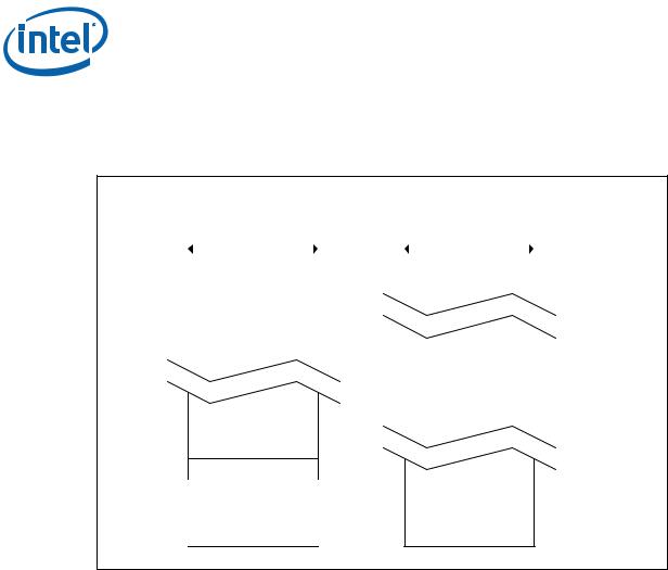
2.1.3.2Dual-Channel Mode - Intel® Flex Memory Technology Mode
The IMC supports Intel® Flex Memory Technology Mode. This mode combines the advantages of the Dual-Channel Symmetric (Interleaved) and Dual-Channel Asymmetric Modes. Memory is divided into a symmetric and a asymmetric zone. The symmetric zone starts at the lowest address in each channel and is contiguous until the asymmetric zone begins or until the top address of the channel with the smaller capacity is reached. In this mode, the system runs with one zone of dual-channel mode and one zone of single-channel mode, simultaneously, across the whole memory array.
Figure 2. Intel® Flex Memory Technology Operation
C |
B |
C H A |
B
C H A
B |
C H B |
C |
B |
C H B |
|
T O M |
C |
N o n in te rle a v e d |
|
a c c e s s |
B |
|
|
D u a l c h a n n e l |
|
in te rle a v e d a c c e s s |
B |
|
B – T h e la rg e s t p h y s ic a l m e m o ry a m o u n t o f th e s m a lle r s iz e m e m o ry m o d u le
C– T h e re m a in in g p h y s ic a l m e m o ry a m o u n t o f th e la rg e r s iz e m e m o ry m o d u le
2.1.3.2.1Dual-Channel Symmetric Mode
Dual-Channel Symmetric mode, also known as interleaved mode, provides maximum performance on real world applications. Addresses are ping-ponged between the channels after each cache line (64-byte boundary). If there are two requests, and the second request is to an address on the opposite channel from the first, that request can be sent before data from the first request has returned. If two consecutive cache lines are requested, both may be retrieved simultaneously, since they are ensured to be on opposite channels. Use Dual-Channel Symmetric mode when both Channel A and Channel B DIMM connectors are populated in any order, with the total amount of memory in each channel being the same.
When both channels are populated with the same memory capacity and the boundary between the dual channel zone and the single channel zone is the top of memory, IMC operates completely in Dual-Channel Symmetric mode.
Note: The DRAM device technology and width may vary from one channel to the other.
2.1.3.2.2Dual-Channel Asymmetric Mode
This mode trades performance for system design flexibility. Unlike the previous mode, addresses start at the bottom of Channel B and stay there until the end of the highest rank in Channel B, and then addresses continue from the bottom of Channel A to the top. Real world applications are unlikely to make requests that alternate between addresses that sit on opposite channels with this memory organization, so in most cases, bandwidth is limited to a single channel.
Intel® CoreTM i7-660UE, i7-620LE/UE, i7-610E, i5-520E, i3-330E and Intel® Celeron® Processor P4505, U3405 Series
August 2010 |
Datasheet Addendum |
Document Number: 323178-003 |
17 |
Interfaces
This mode is used when Intel® Flex Memory Technology is disabled and both Channel A and Channel B DIMM connectors are populated in any order with the total amount of memory in each channel being different.
Figure 3. Dual-Channel Symmetric (Interleaved) and Dual-Channel Asymmetric Modes
Dual Channel Interleaved |
Dual Channel Asymmetric |
||||||||
(memory sizes must match) |
(memory sizes can differ) |
||||||||
|
|
CL |
Top of |
|
|
CL |
|
Top of |
|
|
|
|
|
|
|
|
|
||
|
|
CH. B |
Memory |
|
|
CH. A |
|
Memory |
|
|
|
|
|
|
|
|
|||
|
|
|
|
|
|
|
|
|
|
|
|
CH. A |
|
|
|
|
|
|
|
|
|
|
|
|
|
|
|
|
CH.B-top |
|
|
|
|
|
|
|
|
|
|
|
|
|
|
|
|
|
|
|
|
|
|
|
|
|
|
|
CH. B |
|
DRB |
|
|
|
|
|
|
|
|
|
|
CH. B |
|
CH. A |
|
CH. B |
|
CH. A |
0 |
0 |
2.1.4Rules for Populating Memory Slots
In all modes, the frequency of system memory is the lowest frequency of all memory modules placed in the system, as determined through the SPD registers on the memory modules. The system memory controller supports only one DIMM connector per channel.For dual-channel modes both channels must have an DIMM connector populated and for single-channel mode only a single-channel must have an DIMM connector populated.
2.1.5Technology Enhancements of Intel® Fast Memory Access (Intel® FMA)
The following sections describe the Just-in-Time Scheduling, Command Overlap, and Out-of-Order Scheduling Intel® FMA technology enhancements.
2.1.5.1Just-in-Time Command Scheduling
The memory controller has an advanced command scheduler where all pending requests are examined simultaneously to determine the most efficient request to be issued next. The most efficient request is picked from all pending requests and issued to system memory Just-in-Time to make optimal use of Command Overlapping. Thus, instead of having all memory access requests go individually through an arbitration mechanism forcing requests to be executed one at a time, they can be started without
Intel® CoreTM i7-660UE, i7-620LE/UE, i7-610E, i5-520E, i3-330E and Intel® Celeron® Processor P4505, U3405 Series
Datasheet Addendum |
August 2010 |
18 |
Document Number: 323178-003 |

Interfaces
interfering with the current request allowing for concurrent issuing of requests. This allows for optimized bandwidth and reduced latency while maintaining appropriate command spacing to meet system memory protocol.
2.1.5.2Command Overlap
Command Overlap allows the insertion of the DRAM commands between the Activate, Precharge, and Read/Write commands normally used, as long as the inserted commands do not affect the currently executing command. Multiple commands can be issued in an overlapping manner, increasing the efficiency of system memory protocol.
2.1.5.3Out-of-Order Scheduling
While leveraging the Just-in-Time Scheduling and Command Overlap enhancements, the IMC continuously monitors pending requests to system memory for the best use of bandwidth and reduction of latency. If there are multiple requests to the same open page, these requests would be launched in a back to back manner to make optimum use of the open memory page. This ability to reorder requests on the fly allows the IMC to further reduce latency and increase bandwidth efficiency.
2.1.6DRAM Clock Generation
Two differential clock pairs for every supported DIMM. There are total of four clock pairs driven directly by the processor to two DIMMs.
2.1.7DDR3 On-Die Termination
On-Die Termination (ODT) is a feature that allows a DRAM device to turn on/off internal termination resistance for each DQ, DQS/DQS#, and DM signal via the ODT control pin.
The ODT feature improves signal integrity of the memory channel by allowing the DRAM controller to independently turn on or off the termination resistance for any or all DRAM devices themselves instead of on the motherboard.
The IMC drives out the required ODT signals, based on the memory configuration and which rank is being written to or read from, to the DRAM devices on a targeted DIMM module rank to enable or disable their termination resistance.
2.2PCI Express* Interface
This section describes the PCI Express* interface capabilities of the processor. See the PCI Express Base Specification for further details on PCI Express.
The processor has two options for PCI Express controllers available:
•1 x16 PCI Express Port or
•2 x8 PCI Express Ports
—Enabled with CFG[0] strapping, see Section 2.2.2 and Section 3.2
2.2.1PCI Express* Configuration Mechanism
The PCI Express* link is mapped through a PCI-to-PCI bridge structure.
Intel® CoreTM i7-660UE, i7-620LE/UE, i7-610E, i5-520E, i3-330E and Intel® Celeron® Processor P4505, U3405 Series
August 2010 |
Datasheet Addendum |
Document Number: 323178-003 |
19 |

Interfaces
Figure 4. PCI Express* Related Register Structures in the
Intel® CoreTM i7-660UE, i7-620LE/UE, i7-610E, i5-520E, i3-330E and Intel® Celeron® Processor P4505, U3405 Series
|
|
|
|
|
|
|
|
PCI Express |
Port 0 |
|
PCI-PCI Bridge |
|
PCI Compatible |
|
|
|
representing root |
|
|
||||
Device |
|
|
PCI Express port |
|
Host Bridge Device |
|
|
|
|
|
|
||||
|
|
|
(Device 0) |
|
|||
|
|
|
(Device 1) |
|
|
||
|
|
|
|
|
|
|
|
|
|
|
|
|
|
|
|
|
|
|
|
|
|
|
|
PCI Express |
Port 1 |
|
PCI-PCI Bridge |
|
|
|
|
|
representing root |
|
|
|
|
||
Device |
|
|
PCI Express port |
|
|
|
|
|
|
|
(Device 6) |
|
|
|
|
|
|
|
|
|
|
|
|
|
|
|
|
|
|
|
|
|
|
|
|
|
|
|
|
|
|
|
|
|
DMI |
||
2.2.2PCI Express Port Bifurcation
When bifurcated, the wires which had previously been assigned to lanes 15:8 of the single x16 primary port (Port 0) are reassigned to lanes 7:0 of the x8 secondary port (Port 1). This assignment applies whether the lane numbering is reversed or not. The controls for the secondary port (Port 1) and the associated virtual PCI-to-PCI bridge can be found in PCI Device 6.
When the primary port is not bifurcated, Device 6 is hidden from the discovery mechanism used in PCI enumeration, such that configuration of the device is neither possible nor necessary.
Intel® CoreTM i7-660UE, i7-620LE/UE, i7-610E, i5-520E, i3-330E and Intel® Celeron® Processor P4505, U3405 Series
Datasheet Addendum |
August 2010 |
20 |
Document Number: 323178-003 |
Signal Description
3 |
Signal Description |
|||
|
|
|
|
|
|
This chapter describes the processor signals. They are arranged in functional groups |
|||
|
according to their associated interface or category. The following notations are used to |
|||
|
describe the signal type: |
|||
|
|
|
|
|
|
Notations |
|
Signal Type |
|
|
|
|
|
|
|
I |
|
Input Pin |
|
|
|
|
|
|
|
O |
|
Output Pin |
|
|
|
|
|
|
|
I/O |
|
Bi-directional Input/Output Pin |
|
|
|
|
|
|
|
The signal description also includes the type of buffer used for the particular signal: |
|||
Table 6. |
Signal Description Buffer Types |
|||
|
|
|
|
|
|
Signal |
|
Description |
|
|
|
|
||
|
|
PCI Express interface signals. These signals are compatible with PCI Express 2.0 |
||
|
PCI Express* |
Signalling Environment AC Specifications and are AC coupled. The buffers are not 3.3- |
||
|
|
V tolerant. Refer to the PCIe specification. |
||
|
|
|
||
|
|
Intel Flexible Display interface signals. These signals are compatible with PCI Express |
||
|
FDI |
2.0 Signaling Environment AC Specifications, but are DC coupled. The buffers are not |
||
|
|
3.3-V tolerant. |
||
|
|
|
||
|
|
Direct Media Interface signals. These signals are compatible with PCI Express 2.0 |
||
|
DMI |
Signaling Environment AC Specifications, but are DC coupled. The buffers are not 3.3- |
||
|
|
V tolerant. |
||
|
|
|
||
|
CMOS |
CMOS buffers. 1.1-V tolerant |
||
|
|
|
||
|
DDR3 |
DDR3 buffers: 1.5-V tolerant |
||
|
|
|
||
|
A |
Analog reference or output. May be used as a threshold voltage or for buffer |
||
|
compensation. |
|||
|
|
|||
|
|
|
||
|
GTL |
Gunning Transceiver Logic signaling technology. |
||
|
|
|
||
|
Ref |
Voltage reference signal. |
||
|
|
|
||
|
Asynchronous1 |
Signal has no timing relationship with any reference clock. |
||
NOTES:
1. Qualifier for a buffer type.
3.1System Memory Interface
Table 7. |
Memory Channel A (Sheet 1 of 2) |
|
|
|
|
|
|
|
Signal Name |
Description |
Direction/Buffer |
|
Type |
||
|
|
|
|
|
|
|
|
|
SA_BS[2:0] |
Bank Select: These signals define which banks |
O |
|
are selected within each SDRAM rank. |
DDR3 |
|
|
|
||
|
|
|
|
|
|
Write Enable Control Signal: Used with |
O |
|
SA_WE# |
SA_RAS# and SA_CAS# (along with SA_CS#) to |
|
|
DDR3 |
||
|
|
define the SDRAM Commands. |
|
|
|
|
|
|
|
|
|
Intel® CoreTM i7-660UE, i7-620LE/UE, i7-610E, i5-520E, i3-330E and Intel® Celeron® Processor P4505, U3405 Series
August 2010 |
Datasheet Addendum |
Document Number: 323178-003 |
21 |

Signal Description
Table 7. |
Memory Channel A (Sheet 2 of 2) |
|
|
|
|
|
|
|
Signal Name |
Description |
Direction/Buffer |
|
Type |
||
|
|
|
|
|
|
|
|
|
|
RAS Control Signal: Used with SA_CAS# and |
O |
|
SA_RAS# |
SA_WE# (along with SA_CS#) to define the SRAM |
|
|
DDR3 |
||
|
|
Commands. |
|
|
|
|
|
|
|
|
|
|
|
CAS Control Signal: Used with SA_RAS# and |
O |
|
SA_CAS# |
SA_WE# (along with SA_CS#) to define the SRAM |
|
|
DDR3 |
||
|
|
Commands. |
|
|
|
|
|
|
|
|
|
|
|
Data Mask: These signals are used to mask |
|
|
|
individual bytes of data in the case of a partial |
O |
|
SA_DM[7:0] |
write and to interrupt burst writes. When activated |
|
|
during writes, the corresponding data groups in |
DDR3 |
|
|
|
||
|
|
the SDRAM are masked. There is one SA_DM[7:0] |
|
|
|
for every data byte lane. |
|
|
|
|
|
|
|
ECC Data Strobe: SA_DQS[8] is the data strobe |
I/O |
|
SA_DQS[8] |
for the ECC check data bits SA_DQ[71:64] |
|
|
DDR3 |
||
|
|
Note: Not required for non-ECC mode |
|
|
|
|
|
|
|
|
|
|
|
Data Strobes: SA_DQS[7:0] and its complement |
|
|
SA_DQS[7:0] |
signal group make up a differential strobe pair. The |
I/O |
|
data is captured at the crossing point of |
||
|
DDR3 |
||
|
|
SA_DQS[7:0] and its SA_DQS#[7:0] during read |
|
|
|
|
|
|
|
and write transactions |
|
|
|
|
|
|
|
ECC Data Strobe Complement: SA_DQS#[8] is |
|
|
SA_DQS#[8] |
the complement strobe for the ECC check data bits |
I/O |
|
SA_DQ[71:64] |
DDR3 |
|
|
|
||
|
|
Note: Not required for non-ECC mode |
|
|
|
|
|
|
SA_DQS#[7:0] |
Data Strobe Complements: These are the |
I/O |
|
complementary strobe signals. |
DDR3 |
|
|
|
||
|
|
|
|
|
|
ECC Check Data Bits: SA_DQ[71:64] are the ECC |
I/O |
|
SA_DQ[71:64] |
check data bits for Channel A. |
|
|
DDR3 |
||
|
|
Note: Not required for non-ECC mode |
|
|
|
|
|
|
|
|
|
|
SA_DQ[63:0] |
Data Bus: Channel A data signal interface to the |
I/O |
|
SDRAM data bus. |
DDR3 |
|
|
|
||
|
|
|
|
|
|
Memory Address: These signals are used to |
O |
|
SA_MA[15:0] |
provide the multiplexed row and column address |
|
|
DDR3 |
||
|
|
to the SDRAM. |
|
|
|
|
|
|
|
|
|
|
|
SDRAM Differential Clock: Channel A SDRAM |
|
|
SA_CK[1:0] |
Differential clock signal pair. The crossing of the |
O |
|
positive edge of SA_CK and the negative edge of |
||
|
DDR3 |
||
|
|
its complement SA_CK# are used to sample the |
|
|
|
|
|
|
|
command and control signals on the SDRAM. |
|
|
|
|
|
|
SA_CK#[1:0] |
SDRAM Inverted Differential Clock: Channel A |
O |
|
SDRAM Differential clock signal-pair complement. |
DDR3 |
|
|
|
||
|
|
|
|
|
|
Clock Enable: (1 per rank) Used to: |
|
|
|
- Initialize the SDRAMs during power-up |
O |
|
SA_CKE[1:0] |
- Power-down SDRAM ranks |
|
|
DDR3 |
||
|
|
- Place all SDRAM ranks into and out of self-refresh |
|
|
|
|
|
|
|
during STR |
|
|
|
|
|
|
|
Chip Select: (1 per rank) Used to select particular |
O |
|
SA_CS#[1:0] |
SDRAM components during the active state. There |
|
|
DDR3 |
||
|
|
is one Chip Select for each SDRAM rank. |
|
|
|
|
|
|
|
|
|
|
SA_ODT[1:0] |
On Die Termination: Active Termination Control. |
O |
|
DDR3 |
||
|
|
|
|
|
|
|
|
Intel® CoreTM i7-660UE, i7-620LE/UE, i7-610E, i5-520E, i3-330E and Intel® Celeron® Processor P4505, U3405 Series
Datasheet Addendum |
August 2010 |
22 |
Document Number: 323178-003 |

Signal Description
Table 8. |
Memory Channel B (Sheet 1 of 2) |
|
|
|
|
|
|
|
Signal Name |
Description |
Direction/Buffer |
|
Type |
||
|
|
|
|
|
|
|
|
|
SB_BS[2:0] |
Bank Select: These signals define which banks |
O |
|
are selected within each SDRAM rank. |
DDR3 |
|
|
|
||
|
|
|
|
|
|
Write Enable Control Signal: Used with |
O |
|
SB_WE# |
SB_RAS# and SB_CAS# (along with SB_CS#) to |
|
|
DDR3 |
||
|
|
define the SDRAM Commands. |
|
|
|
|
|
|
|
|
|
|
|
RAS Control Signal: Used with SB_CAS# and |
O |
|
SB_RAS# |
SB_WE# (along with SB_CS#) to define the SRAM |
|
|
DDR3 |
||
|
|
Commands. |
|
|
|
|
|
|
|
|
|
|
|
CAS Control Signal: Used with SB_RAS# and |
O |
|
SB_CAS# |
SB_WE# (along with SB_CS#) to define the SRAM |
|
|
DDR3 |
||
|
|
Commands. |
|
|
|
|
|
|
|
|
|
|
|
Data Mask: These signals are used to mask |
|
|
|
individual bytes of data in the case of a partial |
O |
|
SB_DM[7:0] |
write, and to interrupt burst writes. When |
|
|
activated during writes, the corresponding data |
DDR3 |
|
|
|
||
|
|
groups in the SDRAM are masked. There is one |
|
|
|
SB_DM[7:0] for every data byte lane. |
|
|
|
|
|
|
|
ECC Data Strobe: SB_DQS[8] is the data strobe |
I/O |
|
SB_DQS[8] |
for the ECC check data bits SB_DQ[71:64] |
|
|
DDR3 |
||
|
|
Note: Not required for non-ECC mode |
|
|
|
|
|
|
|
|
|
|
|
Data Strobes: SB_DQS[7:0] and its complement |
|
|
|
signal group make up a differential strobe pair. The |
I/O |
|
SB_DQS[7:0] |
data is captured at the crossing point of |
|
|
DDR3 |
||
|
|
SB_DQS[7:0] and its SB_DQS#[7:0] during read |
|
|
|
|
|
|
|
and write transactions. |
|
|
|
|
|
|
|
ECC Data Strobe Complement: SB_DQS#[8] is |
|
|
SB_DQS#[8] |
the complement strobe for the ECC check data bits |
I/O |
|
SB_DQ[71:64] |
DDR3 |
|
|
|
||
|
|
Note: Not required for non-ECC mode |
|
|
|
|
|
|
SB_DQS#[7:0] |
Data Strobe Complements: These are the |
I/O |
|
complementary strobe signals. |
DDR3 |
|
|
|
||
|
|
|
|
|
|
ECC Check Data Bits: SB_DQ[71:64] are the ECC |
I/O |
|
SB_DQ[71:64] |
check data bits for Channel B |
|
|
DDR3 |
||
|
|
Note: Not required for non-ECC mode |
|
|
|
|
|
|
|
|
|
|
SB_DQ[63:0] |
Data Bus: Channel B data signal interface to the |
I/O |
|
SDRAM data bus. |
DDR3 |
|
|
|
||
|
|
|
|
|
|
Memory Address: These signals are used to |
O |
|
SB_MA[15:0] |
provide the multiplexed row and column address |
|
|
DDR3 |
||
|
|
to the SDRAM. |
|
|
|
|
|
|
|
|
|
|
|
SDRAM Differential Clock: Channel B SDRAM |
|
|
|
Differential clock signal pair. The crossing of the |
O |
|
SB_CK[1:0] |
positive edge of SB_CK and the negative edge of |
|
|
DDR3 |
||
|
|
its complement SB_CK# are used to sample the |
|
|
|
|
|
|
|
command and control signals on the SDRAM. |
|
|
|
|
|
|
SB_CK#[1:0] |
SDRAM Inverted Differential Clock: Channel B |
O |
|
SDRAM Differential clock signal-pair complement. |
DDR3 |
|
|
|
||
|
|
|
|
|
|
Clock Enable: (1 per rank) Used to: |
|
|
|
- Initialize the SDRAMs during power-up. |
O |
|
SB_CKE[1:0] |
- Power-down SDRAM ranks. |
|
|
DDR3 |
||
|
|
- Place all SDRAM ranks into and out of self-refresh |
|
|
|
|
|
|
|
during STR. |
|
|
|
|
|
|
|
Chip Select: (1 per rank) Used to select particular |
O |
|
SB_CS#[1:0] |
SDRAM components during the active state. There |
|
|
DDR3 |
||
|
|
is one Chip Select for each SDRAM rank. |
|
|
|
|
|
|
|
|
|
Intel® CoreTM i7-660UE, i7-620LE/UE, i7-610E, i5-520E, i3-330E and Intel® Celeron® Processor P4505, U3405 Series
August 2010 |
Datasheet Addendum |
Document Number: 323178-003 |
23 |

Signal Description
Table 8. |
Memory Channel B (Sheet 2 of 2) |
|
|
|
|
|
|
|
Signal Name |
Description |
Direction/Buffer |
|
Type |
||
|
|
|
|
|
|
|
|
|
SB_ODT[1:0] |
On Die Termination: Active Termination Control. |
O |
|
DDR3 |
||
|
|
|
|
|
|
|
|
3.2Reset and Miscellaneous Signals
Table 9. |
Reset and Miscellaneous Signals |
|
||
|
|
|
|
|
|
Signal Name |
|
Description |
Direction/Buffer |
|
|
Type |
||
|
|
|
|
|
|
|
|
|
|
|
SM_DRAMRST# |
DDR3 DRAM Reset: Reset signal from processor |
O |
|
|
to DRAM devices. One for all channels of DIMMs. |
DDR3 |
||
|
|
|||
|
|
|
|
|
|
|
Configuration signals: |
|
|
|
|
The CFG signals have a default value of 1 if not |
|
|
|
|
terminated on the board. Refer to the Platform |
|
|
|
|
Design Guide for pull-down recommendations |
|
|
|
|
when logic low is desired. |
|
|
|
|
• CFG[0]: PCI Express* Bifurcation: |
|
|
|
|
— 1 = 1 x16 PCI Express I/O |
|
|
|
|
— 0 = 2 x 8 PCI Express I/O |
|
|
|
|
• CFG[1]: Reserved |
|
|
|
|
• CFG[2]: Reserved configuration lands. A test |
|
|
|
|
point may be placed on the board for this land. |
|
|
|
|
• CFG[3]: PCI Express* Static Lane Numbering |
|
|
|
|
Reversal. A test point may be placed on the |
|
|
|
|
board for this land. Lane reversal will be |
|
|
|
|
applied across all 16 lanes. |
|
|
|
|
— |
1: No Reversal |
|
|
|
— |
0: Reversal |
|
|
CFG[17:0] |
In the case of Bifurcation with NO Lane Reversal |
I |
|
|
CMOS |
|||
|
|
the physical lane mapping is as follows: |
||
|
|
— Lanes 15:8 => Port 1 Lanes 7:0 |
|
|
|
|
— Lanes 7:0 => Port 0 Lanes 7:0 |
|
|
|
|
In the case of Bifurcation with WITH Lane Reversal |
|
|
|
|
the physical lane mapping is as follows: |
|
|
|
|
— Lanes 15:8 => Port 0 Lanes 0:7 |
|
|
|
|
— Lanes 7:0 => Port 1 Lanes 0:7 |
|
|
|
|
• CFG[4]: Embedded DisplayPort Detection: |
|
|
|
|
This is used to detect the presence of a device |
|
|
|
|
on the Embedded DisplayPort. |
|
|
|
|
— 1: No Physical Display Port attached to |
|
|
|
|
|
the Embedded Display Port |
|
|
|
— 0: An external Display Port device is |
|
|
|
|
|
connected to the Embedded Display Port |
|
|
|
• CFG[17:5]: Reserved configuration lands. |
|
|
|
|
Intel does not recommend a test point on the |
|
|
|
|
board for these lands. |
|
|
|
|
|
|
|
§ §
Intel® CoreTM i7-660UE, i7-620LE/UE, i7-610E, i5-520E, i3-330E and Intel® Celeron® Processor P4505, U3405 Series
Datasheet Addendum |
August 2010 |
24 |
Document Number: 323178-003 |

Electrical Specifications
4 Electrical Specifications
4.1Signal Groups
Signals are grouped by buffer type and similar characteristics as listed in Table 10. The buffer type indicates which signaling technology and specifications apply to the signals. All the differential signals, and selected DDR3 and Control Sideband signals have OnDie Termination (ODT) resistors. There are some signals that do not have ODT and need to be terminated on the board.
Table 10. |
Mobile Signal Groups1 |
|
|
|
|
Signal Group |
Alpha |
Type |
Signals |
|
Group |
|||
|
|
|
|
|
|
|
|
|
|
|
DDR3 Data Signals2 |
|
|
|
|
Single ended |
(e) |
DDR3 Bi-directional |
SA_DQ[71:0], SB_DQ[71:0] |
|
|
|
|
|
|
Differential |
(f) |
DDR3 Bi-directional |
SA_DQS[8:0], SA_DQS#[8:0] |
|
|
|
|
SB_DQS[8:0], SB_DQS#[8:0] |
|
|
|
|
|
|
Power/Ground/Other |
|
|
|
|
|
|
|
|
|
Single Ended |
(z) |
Other |
DBR#, PROC_DETECT, VCAP0, VCAP1, VCAP2 |
|
|
|
|
|
|
NOTES: |
|
|
|
1.Refer to Chapter 3 for signal description details.
2.SA and SB refer to DDR3 Channel A and DDR3 Channel B.
All Control Sideband Asynchronous signals are required to be asserted/deasserted for at least eight BCLKs in order for the processor to recognize the proper signal state. See Section 4.2 for the DC specifications.
4.2DC Specifications
The processor DC specifications in this section are defined at the processor pins, unless noted otherwise. See Chapter 5 for the processor pin listings and Chapter 3 for signal definitions.
The DC specifications for the DDR3 signals are listed in Table 11.
4.2.1Voltage and Current Specifications
Table 11. |
DDR3 Signal Group DC Specifications (Sheet 1 of 2) |
|
|
|
|||
|
|
|
|
|
|
|
|
Symbol |
Parameter |
Alpha |
Min |
Typ |
Max |
Units |
Notes1,9 |
|
|
Group |
|
|
|
|
|
|
|
|
|
|
|
|
|
VIL |
Input Low Voltage |
(e,f) |
|
|
0.43*VDDQ |
V |
2,4 |
NOTES: |
|
|
|
|
|
|
|
1.Unless otherwise noted, all specifications in this table apply to all processor frequencies.
2.VIL is defined as the maximum voltage level at a receiving agent that will be interpreted as a logical low value.
3.VIH is defined as the minimum voltage level at a receiving agent that will be interpreted as a logical high value.
4.VIH and VOH may experience excursions above VDDQ. However, input signal drivers must comply with the signal quality specifications.
5.RVTT_TERM is the termination on the DIMM and in not controlled by the processor.
Intel® CoreTM i7-660UE, i7-620LE/UE, i7-610E, i5-520E, i3-330E and Intel® Celeron® Processor P4505, U3405 Series
August 2010 |
Datasheet Addendum |
Document Number: 323178-003 |
25 |

Electrical Specifications
Table 11. |
DDR3 Signal Group DC Specifications (Sheet 2 of 2) |
|
|
|
|
|||
|
|
|
|
|
|
|
|
|
Symbol |
Parameter |
Alpha |
Min |
Typ |
|
Max |
Units |
Notes1,9 |
|
|
Group |
|
|
|
|
|
|
|
|
|
|
|
|
|
|
|
VIH |
Input High Voltage |
(e,f) |
0.57*VDDQ |
|
|
|
V |
3 |
VOL |
Output Low Voltage |
(c,d,e,f) |
|
(VDDQ / 2)* (RON |
/ |
|
|
5 |
|
(RON+RVTT_TERM)) |
|
|
|||||
|
|
|
|
|
|
|
||
VOH |
|
|
|
VDDQ - ((VDDQ / 2)* |
|
|
|
|
Output High Voltage |
(c,d,e,f) |
|
(RON/ |
|
|
V |
4,5 |
|
|
|
|
|
(RON+RVTT_TERM)) |
|
|
|
|
NOTES:
1.Unless otherwise noted, all specifications in this table apply to all processor frequencies.
2.VIL is defined as the maximum voltage level at a receiving agent that will be interpreted as a logical low value.
3.VIH is defined as the minimum voltage level at a receiving agent that will be interpreted as a logical high value.
4.VIH and VOH may experience excursions above VDDQ. However, input signal drivers must comply with the signal quality specifications.
5.RVTT_TERM is the termination on the DIMM and in not controlled by the processor.
Intel® CoreTM i7-660UE, i7-620LE/UE, i7-610E, i5-520E, i3-330E and Intel® Celeron® Processor P4505, U3405 Series
Datasheet Addendum |
August 2010 |
26 |
Document Number: 323178-003 |

Processor Ball and Signal Information
5Processor Ball and Signal Information
5.1Processor Ball Assignments
•Table 12 provides a listing of all processor pins ordered alphabetically by ball name for the Intel® CoreTM i7-660UE, i7-620LE/UE, i7-610E, i5-520E, i3-330E and Intel® Celeron® Processor P4505, U3405 Series package respectively.
•Table 13 provides a listing of all processor pins ordered alphabetically by ball number for the Intel® CoreTM i7-660UE, i7-620LE/UE, i7-610E, i5-520E, i3-330E and Intel® Celeron® Processor P4505, U3405 Series package respectively.
•Figure 5, Figure 6, Figure 7, and Figure 8 show the Top-Down view of the Intel® CoreTM i7-660UE, i7-620LE/UE, i7-610E, i5-520E, i3-330E and Intel® Celeron® Processor P4505, U3405 Series ballmap
Intel® CoreTM i7-660UE, i7-620LE/UE, i7-610E, i5-520E, i3-330E and Intel® Celeron® Processor P4505, U3405 Series
August 2010 |
Datasheet Addendum |
Document Number: 323178-003 |
27 |

Processor Ball and Signal Information
Figure 5. Intel® CoreTM i7-660UE, i7-620LE/UE, i7-610E, i5-520E, i3-330E and Intel® Celeron® Processor P4505, U3405 Series Ballmap (Top View, Upper-Left Quadrant)
|
71 |
70 |
69 |
68 |
67 |
66 |
65 |
64 |
63 |
62 |
61 |
|
60 |
|
59 |
58 |
57 |
56 |
55 |
54 |
53 |
52 |
51 |
50 |
49 |
48 |
47 |
46 |
45 |
44 |
43 |
42 |
41 |
40 |
39 |
38 |
37 |
36 |
|
|
BV |
DC_TES |
|
DC_TES |
DC_TES |
|
VSS |
|
VSS |
|
SB_DQS SB_DQ[4 |
|
|
SB_DQ[4 |
|
SB_DM[5 |
|
SB_DQS SB_DQ[3 |
|
SB_DQ[3 |
|
SB_DQ[3 |
|
SB_DQ[3 SB_DM[4 |
|
SB_ODT |
|
SB_BS[1 |
|
SB_BS[0 |
SM_RCO |
|
SB_CK[1 |
|
|
SA_MA[2 |
|
||||
T_BV71 |
|
T_BV69 |
T_BV68 |
|
|
|
[6] |
8] |
|
|
|
7] |
|
] |
|
#[5] |
9] |
|
7] |
|
4] |
|
3] |
] |
|
[0] |
|
] |
|
] |
MP[2] |
|
] |
|
|
] |
|
|||
BU |
|
|
|
|
|
|
SB_DM[6 |
|
SB_DQS |
VSS |
|
|
SB_DQ[4 |
|
VSS |
|
SB_DQS |
VSS |
|
SB_DQ[4 |
|
VSS |
|
SB_ODT |
VSS |
|
SB_CAS |
|
VSS |
|
SB_MA[1 |
|
SA_DQ[6 |
SB_CK#[ |
|
|
VSS |
|
|
|
|
|
|
|
|
|
] |
|
#[6] |
|
|
6] |
|
|
|
[5] |
|
1] |
|
|
[1] |
|
# |
|
|
0] |
|
6] |
1] |
|
|
|
|
||||||||
|
|
|
|
|
|
|
|
|
|
|
|
|
|
|
|
|
|
|
|
|
|
|
|
|
|
|
|
|
|
|
|
|
|
|
|
|
|
|
|
|
BT |
DC_TES |
|
DC_TES |
VSS |
|
|
|
|
|
|
SB_DQ[5 |
|
|
|
SB_DQ[4 |
|
SB_DQ[4 |
|
SB_DQ[4 SB_DQ[3 |
|
SB_DQS |
|
SB_DQS |
|
SB_DQ[3 SB_DQ[3 |
|
SB_MA[1 |
|
SB_CS#[ |
|
SB_WE# |
SB_RAS |
|
SA_BS[0] |
|
|
SA_MA[0 |
|
||
T_BT71 |
|
T_BT69 |
|
|
|
|
|
|
|
3] |
|
|
|
2] |
|
3] |
|
4] |
8] |
|
[4] |
|
#[4] |
|
2] |
6] |
|
3] |
|
1] |
|
|
# |
|
|
|
|
] |
|
|
BR |
DC_TES |
|
VSS |
VSS |
|
SB_DQ[5 |
|
SB_DQ[5 |
|
SB_DQ[5 |
|
|
|
|
|
|
|
|
|
|
|
|
|
|
|
|
|
|
|
|
|
|
|
|
|
|
|
|
|
|
T_BR71 |
|
|
0] |
|
1] |
|
2] |
|
|
|
|
|
|
|
|
|
|
|
|
|
|
|
|
|
|
|
|
|
|
|
|
|
|
|
|
|
|
|||
BP |
|
|
|
|
|
|
|
|
|
|
|
|
SB_DQ[4 |
|
SA_DQS |
|
SB_DQ[4 |
|
|
SB_DQ[4 |
|
|
|
SB_DQ[3 |
|
|
SB_CS#[ |
|
|
|
VSS |
|
|
SM_RCO |
|
|
|
|
|
|
|
|
|
|
|
|
|
|
|
|
|
|
9] |
|
|
#[6] |
|
5] |
|
|
0] |
|
|
|
5] |
|
|
0] |
|
|
|
|
|
MP[1] |
|
|
|
|
|
||
BN |
VSS |
|
|
SB_DQ[5 |
|
|
SA_DQ[5 |
VSS |
|
SA_DM[6 |
|
|
|
|
|
|
SA_DQ[4 |
|
SA_DQ[4 |
|
|
|
SA_DQ[4 |
|
|
SA_DQ[4 SA_DQ[3 |
|
|
SA_DQ[3 |
|
|
|
SA_DQ[3 |
|
SB_DQ[6 |
|
|
|
|
|
|
|
4] |
|
|
0] |
|
] |
|
|
|
|
|
|
9] |
|
7] |
|
|
|
1] |
|
|
0] |
9] |
|
|
8] |
|
|
|
6] |
|
8] |
|
|
|
|
|||
BM |
|
VSS |
|
|
|
|
|
|
|
|
|
|
SA_DQS[ |
|
|
|
|
|
|
SA_DQ[4 |
|
VSS |
|
|
|
|
|
|
VSS |
SA_DQ[3 |
|
|
|
|
|
|
|
|
|
|
|
|
|
|
|
|
|
|
|
|
|
6] |
|
|
|
|
|
|
|
6] |
|
|
|
|
|
|
|
3] |
|
|
|
|
|
|
|
|
|
||||
BL |
VSS |
|
SB_DQ[5 |
|
|
|
|
|
|
|
|
|
|
|
|
|
VSS |
|
VSS |
|
|
|
|
|
|
VSS |
SA_ODT[ |
|
|
|
|
|
|
VSS |
|
SA_RAS |
|
|
|
|
|
5] |
|
|
|
|
|
|
|
|
|
|
|
|
|
|
|
|
|
|
|
|
1] |
|
|
|
|
|
|
|
# |
|
|
|
|
||||||
|
|
|
|
|
|
|
|
|
|
|
|
|
|
|
|
|
|
|
|
|
|
|
|
|
|
|
|
|
|
|
|
|
|
|
|
|||||
BK |
|
SB_DQ[6 |
|
|
SB_DQ[6 |
|
|
SA_DQ[5 |
VSS |
|
SA_DQ[5 |
|
VSS |
|
|
|
|
|
|
VSS |
|
SA_DQS |
|
|
|
|
|
|
SA_DQS[ SA_CAS |
|
|
|
|
|
|
|
SA_CK#[ |
|
||
|
0] |
|
|
1] |
|
|
4] |
|
5] |
|
|
|
|
|
|
|
|
#[5] |
|
|
|
|
|
|
4] |
# |
|
|
|
|
|
|
|
1] |
|
|||||
BJ |
SB_DQ[5 |
|
SB_DQS |
|
|
SA_DQ[6 |
|
VSS |
SA_DQ[5 |
|
SA_DQ[5 |
|
|
|
|
|
SA_DQ[5 |
|
SA_DQ[4 |
|
|
|
|
|
|
SA_DQ[4 SA_CS#[ |
|
|
|
|
|
|
SA_DQ[3 |
|
SA_DQ[7 |
|
|
|
|
|
6] |
|
[7] |
|
|
0] |
|
6] |
|
1] |
|
|
|
|
|
3] |
|
3] |
|
|
|
|
|
|
5] |
1] |
|
|
|
|
|
|
2] |
|
1] |
|
|
|
|
||
BH |
|
VSS |
|
|
|
|
|
|
|
|
|
|
|
|
SA_DM[7 |
|
VSS |
|
VSS |
|
SA_DQ[4 |
|
SA_DQS[ |
|
|
SA_DQ[4 |
VSS |
|
|
SA_DQS SA_DQ[3 |
|
|
SA_CS#[ |
|
SA_BS[1] |
|
|
SA_CK[1 |
|
|
|
|
|
|
|
|
|
|
|
|
|
|
|
] |
|
|
|
2] |
|
5] |
|
|
4] |
|
|
#[4] |
7] |
|
|
0] |
|
|
|
] |
|
||||||
BG |
SB_DQ[5 |
|
SB_DQS |
|
|
|
|
|
|
|
|
|
|
|
|
|
|
|
|
|
SA_DM[5 |
|
VSS |
|
|
|
|
|
|
SA_DM[4 SA_DQ[7 |
|
|
|
|
|
|
|
VSS |
|
|
8] |
|
#[7] |
|
|
|
|
|
|
|
|
|
|
|
|
|
|
|
|
|
] |
|
|
|
|
|
|
|
] |
0] |
|
|
|
|
|
|
|
|
|||
|
|
|
|
|
|
|
|
|
|
|
|
|
|
|
|
|
|
|
|
|
|
|
|
|
|
|
|
|
|
|
|
|
|
|
||||||
BF |
|
SB_DQ[5 |
|
|
SB_DM[7 |
|
SA_DQ[6 SA_DQ[5 |
|
VSS |
|
|
VTT0 |
VTT0 |
|
SA_DQ[5 |
|
SA_DQ[4 |
|
|
|
|
|
|
SA_DQ[3 SA_DQ[3 |
|
|
|
SA_ODT[ |
|
|
SA_MA[1 |
|
SA_WE# |
|
|
|
|
|||
|
7] |
|
|
] |
|
1] |
7] |
|
|
|
|
2] |
|
8] |
|
|
|
|
|
|
5] |
4] |
|
|
|
0] |
|
|
3] |
|
|
|
|
|
||||||
BE |
RSVD |
VSS |
RSVD |
|
|
|
VSS |
SA_DQS[ |
|
SA_DQS |
|
|
|
|
|
|
|
|
|
|
|
|
|
|
|
|
|
|
|
|
|
|
|
|
|
|
|
|
|
|
|
|
|
7] |
|
#[7] |
|
|
|
|
|
|
|
|
|
|
|
|
|
|
|
|
|
|
|
|
|
|
|
|
|
|
|
|
|
|
|||||
BD |
SB_DQ[6 |
|
SB_DQ[6 |
|
|
|
|
|
|
|
|
|
VTT0 |
VTT0 |
|
VSS |
|
VCAP0 |
|
VSS |
|
VCAP0 |
VSS |
|
VCAP0 |
|
VSS |
|
VCAP1 |
|
VSS |
VCAP1 |
|
VSS |
|
|
VCAP1 |
|
|
|
2] |
|
3] |
|
|
|
|
|
|
|
|
|
|
|
|
|
|
|
|
|
|
|
|
|
|
||||||||||||||||
BC |
|
SA_DQ[6 |
|
|
SB_DQ[5 |
|
|
|
|
|
|
|
|
|
|
|
|
|
|
|
|
|
|
|
|
|
|
|
|
|
|
|
|
|
|
|
|
|
|
|
|
3] |
|
|
9] |
|
|
|
|
|
|
|
|
|
|
|
|
|
|
|
|
|
|
|
|
|
|
|
|
|
|
|
|
|
|
|
|
|
|
|
|
BB |
VSS |
|
RSVD |
|
|
SA_DQ[5 |
|
SA_DQ[5 |
|
VSS |
|
|
VTT0 |
VTT0 |
|
VSS |
|
VCAP0 |
|
VSS |
|
VCAP0 |
VSS |
|
VCAP0 |
|
VSS |
|
VCAP1 |
|
VSS |
VCAP1 |
|
VSS |
|
|
VCAP1 |
|
|
|
|
|
|
9] |
|
8] |
|
|
|
|
|
|
|
|
|
|
|
|
|
|
|
|
|||||||||||||||||||
|
|
|
|
|
|
|
|
|
|
|
|
|
|
|
|
|
|
|
|
|
|
|
||||||||||||||||||
BA |
|
VSS |
|
|
|
|
|
|
|
|
|
|
|
|
|
|
|
|
|
|
|
|
|
|
|
|
|
|
|
|
|
|
|
|
|
|
|
|
|
|
AY |
VSS |
|
RSVD |
|
|
VSS |
|
SA_DQ[6 |
|
VSS |
|
|
VTT0 |
VSS |
|
VCAP0 |
|
VSS |
|
VCAP0 |
|
VSS |
VCAP0 |
|
VSS |
|
VCAP1 |
|
VSS |
|
VCAP1 |
VSS |
|
VCAP1 |
|
|
VSS |
|
|
|
|
|
|
|
2] |
|
|
|
|
|
|
|
|
|
|
|
|
|
|
|
|
||||||||||||||||||||
|
|
|
|
|
|
|
|
|
|
|
|
|
|
|
|
|
|
|
|
|
|
|||||||||||||||||||
AW |
|
RSVD |
|
|
VSS |
|
|
|
|
VSS |
|
|
VTT0 |
|
VSS |
|
VCAP0 |
|
VSS |
|
VCAP0 |
|
VSS |
VCAP0 |
|
VSS |
|
VCAP1 |
|
VSS |
|
VCAP1 |
VSS |
|
VCAP1 |
|
|
VSS |
|
|
AV |
RSVD |
|
RSVD |
|
|
PM_EXT |
|
PM_EXT |
|
|
|
|
|
|
|
|
|
|
|
|
|
|
|
|
|
|
|
|
|
|
|
|
|
|
|
|
|
|
|
|
|
|
|
_TS#[0] |
|
_TS#[1] |
|
|
|
|
|
|
|
|
|
|
|
|
|
|
|
|
|
|
|
|
|
|
|
|
|
|
|
|
|
|
|
|
|||
AU |
RSVD |
VSS |
RSVD |
|
|
|
|
|
|
VSS |
|
|
VTT0 |
|
VTT0 |
|
VSS |
|
VCAP0 |
|
VSS |
|
VCAP0 |
VSS |
|
VCAP0 |
|
VSS |
|
VCAP1 |
|
VSS |
VCAP1 |
|
VSS |
|
|
VCAP1 |
|
|
AT |
|
RSVD |
|
|
RSVD |
|
|
VSS |
|
|
|
|
|
|
|
|
|
|
|
|
|
|
|
|
|
|
|
|
|
|
|
|
|
|
|
|
|
|
|
|
AR |
RSVD |
|
RSVD |
|
|
|
|
|
|
VSS |
|
|
VTT0 |
|
VTT0 |
|
VSS |
|
VCAP0 |
|
VSS |
|
VCAP0 |
VSS |
|
VCAP0 |
|
VSS |
|
VCAP1 |
|
VSS |
VCAP1 |
|
VSS |
|
|
VCAP1 |
|
|
AP |
|
VSS |
|
|
|
RSVD |
|
VSS |
|
|
|
|
|
|
|
|
|
|
|
|
|
|
|
|
|
|
|
|
|
|
|
|
|
|
|
|
|
|
|
|
AN |
GFX_VID |
|
RSVD |
|
|
|
|
|
|
VSS |
|
|
VTT0 |
|
VTT0 |
|
VCAP0 |
|
VSS |
|
VCAP0 |
|
VSS |
VCAP0 |
|
VSS |
|
VCAP1 |
|
VSS |
|
VCAP1 |
VSS |
|
VCAP1 |
|
|
VSS |
|
|
[4] |
|
|
|
|
|
|
|
|
|
|
|
|
|
|
|
|
|
|
|
|
|
|
|
|||||||||||||||||
|
|
|
|
|
|
|
|
|
|
|
|
|
|
|
|
|
|
|
|
|
|
|
|
|
||||||||||||||||
|
|
|
|
|
|
|
|
|
|
|
|
|
|
|
|
|
|
|
|
|
|
|
|
|
|
|
|
|
|
|
|
|
|
|
|
|
|
|
|
|
AM |
|
GFX_VID |
|
|
GFX_VID |
RSVD |
|
VSS |
|
|
|
|
|
|
|
|
|
|
|
|
|
|
|
|
|
|
|
|
|
|
|
|
|
|
|
|
|
|
|
|
|
[6] |
|
|
[5] |
|
|
|
|
|
|
|
|
|
|
|
|
|
|
|
|
|
|
|
|
|
|
|
|
|
|
|
|
|
|
|
|
|
|||
AL |
GFX_DP |
|
GFX_IM |
|
|
|
|
|
|
VSS |
|
|
VTT0 |
|
VTT0 |
|
VCAP0 |
|
VSS |
|
VCAP0 |
|
VSS |
VCAP0 |
|
VSS |
|
VCAP1 |
|
VSS |
|
VCAP1 |
VSS |
|
VCAP1 |
|
|
VSS |
|
|
RSLPVR |
|
ON |
|
|
|
|
|
|
|
|
|
|
|
|
|
|
|
|
|
|
|
|
|
|
||||||||||||||||
AK |
RSVD |
VSS |
RSVD |
|
|
RSVD |
|
VSS |
|
VCAP2 |
|
|
VCAP2 |
|
VCAP2 |
|
VCAP0 |
|
VSS |
|
VCAP0 |
|
VSS |
VCAP0 |
|
VSS |
|
VCAP1 |
|
VSS |
|
VCAP1 |
VSS |
|
VCAP1 |
|
|
VSS |
|
|
AJ |
|
VSS |
|
|
|
|
|
|
|
|
|
|
|
|
|
|
|
|
|
|
|
|
|
|
|
|
|
|
|
|
|
|
|
|
|
|
|
|
|
|
AH |
GFX_VID |
|
GFX_VR |
|
|
RSVD |
|
|
|
VSS |
|
|
VCAP2 |
|
VCAP2 |
|
VSS |
|
VSS |
|
VSS |
|
VSS |
VSS |
|
VSS |
|
VSS |
|
VSS |
|
VSS |
VSS |
|
VSS |
|
|
VSS |
|
|
|
[3] |
|
_EN |
|
|
|
|
|
|
|
|
|
|
|
|
|
|
|
|
|
|
|
|
|
|
|
|
|
|
|
|
|
|
|
|
|
|
|
|
|
AG |
|
GFX_VID |
|
|
GFX_VID |
|
|
VSS |
|
|
|
|
|
|
|
|
|
|
|
|
|
|
|
|
|
|
|
|
|
|
|
|
|
|
|
|
|
|
|
|
|
[2] |
|
|
[1] |
|
|
|
|
|
|
|
|
|
|
|
|
|
|
|
|
|
|
|
|
|
|
|
|
|
|
|
|
|
|
|
|
|
|
||
AF |
GFX_VID |
|
VSS |
|
|
|
|
|
|
VSS |
|
|
VCAP2 |
|
VCAP2 |
|
VCC |
|
VCC |
|
VCC |
|
VCC |
VCC |
|
VCC |
|
VCC |
|
VCC |
|
VCC |
VCC |
|
VTT0 |
|
|
VTT0 |
|
|
[0] |
|
|
|
|
|
|
|
|
|
|
|
|
|
|
|
|
|
|
|
|
|
|
|
|||||||||||||||||
AE |
|
VSS |
|
|
|
COMP0 |
|
VSS |
|
|
|
|
|
|
|
|
|
|
|
|
|
|
|
|
|
|
|
|
|
|
|
|
|
|
|
|
|
|
|
|
AD |
COMP3 |
|
COMP1 |
|
|
|
|
|
|
VSS |
|
|
VCAP2 |
|
VCAP2 |
|
VSS |
|
VCC |
|
VSS |
|
VCC |
VSS |
|
VCC |
|
VSS |
|
VCC |
|
VSS |
VCC |
|
VTT0 |
|
|
VTT0 |
|
|
AC |
RSVD |
COMP2 |
RSVD |
|
VSS |
|
|
VSS |
|
|
|
|
|
|
|
|
|
|
|
|
|
|
|
|
|
|
|
|
|
|
|
|
|
|
|
|
|
|
|
|
AB |
|
VSS |
|
|
|
|
|
|
|
VSS |
|
|
VCAP2 |
|
VCAP2 |
|
VSS |
|
VCC |
|
VSS |
|
VCC |
VSS |
|
VCC |
|
VSS |
|
VCC |
|
VSS |
VCC |
|
VSS |
|
|
VSS |
|
|
|
|
|
|
|
|
|
|
|
|
|
|
|
|
|
|
|
|
|
|
|
|
|
|
|||||||||||||||||
323178-003 28

Processor Ball and Signal Information
Figure 6. Intel® CoreTM i7-660UE, i7-620LE/UE, i7-610E, i5-520E, i3-330E and Intel® Celeron® Processor P4505, U3405 Series Ballmap (Top View, Upper-Right Quadrant)
35 |
34 |
33 |
32 |
31 |
30 |
29 |
28 |
27 |
26 |
25 |
24 |
23 |
22 |
21 |
20 |
19 |
18 |
17 |
16 |
15 |
14 |
13 |
12 |
11 |
10 |
9 |
8 |
7 |
6 |
5 |
4 |
3 |
2 |
1 |
|
|
SB_CK#[ |
SM_RCO |
|
SB_MA[4 |
|
SB_MA[2 |
|
SB_MA[8 SB_MA[1 |
|
SB_BS[2 |
|
SB_DQ[2 |
|
SB_DQ[3 SB_DQ[2 |
|
SB_DQ[2 |
|
SB_DQ[1 |
|
SB_DQS SB_DQ[2 |
|
SB_DQ[1 |
|
RSVD_N |
|
RSVD_N |
DC_TES |
|
DC_TES |
|
DC_TES |
|
|||
|
0] |
MP[0] |
|
] |
|
] |
|
] |
4] |
|
] |
|
6] |
|
0] |
9] |
|
2] |
|
9] |
|
[2] |
0] |
|
5] |
|
CTF |
|
CTF |
T_BV5 |
|
T_BV3 |
|
T_BV1 |
|
SA_DQ[6 |
|
SB_CK[0 |
VSS |
|
SB_MA[3 |
|
SB_DQ[7 |
|
SB_MA[1 |
VSS |
|
SB_MA[1 |
|
VSS |
|
SB_DQ[2 |
VSS |
|
SB_DQ[2 |
|
VSS |
|
SB_DQS |
VSS |
|
SB_DQ[1 |
|
VSS |
|
|
|
|
|
|
|
7] |
|
] |
|
] |
|
1] |
|
1] |
|
5] |
|
|
5] |
|
3] |
|
|
#[2] |
|
4] |
|
|
|
|
|
|
|
|
|||||||
|
SB_MA[0 SB_MA[5 |
|
SB_MA[6 |
|
SB_MA[1 |
|
SB_MA[9 SB_CKE[ |
|
SB_CKE[ |
|
SB_DQ[2 |
|
SB_DQ[3 SB_DQS |
|
SB_DQS |
|
SB_DQ[1 |
|
SB_DM[2 SB_DQ[1 |
|
|
|
|
|
|
RSVD_N |
|
DC_TES |
|
DC_TES |
|
||||
|
] |
] |
|
] |
|
2] |
|
] |
0] |
|
1] |
|
7] |
|
1] |
#[3] |
|
[3] |
|
8] |
|
] |
7] |
|
|
|
|
|
|
CTF |
|
T_BT3 |
|
T_BT1 |
|
|
|
|
|
|
|
|
|
|
|
|
|
|
|
|
|
|
|
|
|
|
|
|
|
|
SB_DQ[1 |
|
SB_DQ[1 |
|
SB_DQ[1 |
RSVD_N |
|
VSS |
|
DC_TES |
|
|
|
|
|
|
|
|
|
|
|
|
|
|
|
|
|
|
|
|
|
|
|
|
|
|
6] |
|
1] |
|
0] |
CTF |
|
|
T_BR1 |
|
|
SA_CK#[ |
|
SA_MA[1 |
|
|
SB_MA[1 |
|
|
|
SB_MA[7 |
|
|
|
SB_DM[3 |
|
|
SB_DQ[2 |
|
|
|
SB_DQ[2 |
|
|
SB_DQ[2 |
|
|
|
|
|
|
|
|
|
|
|
|
0] |
|
] |
|
|
] |
|
|
|
] |
|
|
|
] |
|
|
8] |
|
|
|
4] |
|
|
1] |
|
|
|
|
|
|
|
|
|
|
|
|
|
|
|
SA_MA[5 |
|
SA_MA[8 |
|
SA_MA[1 |
|
|
SA_MA[1 SA_DM[3 |
|
|
SA_DQS[ SA_DQ[2 |
|
|
SA_DQ[1 |
|
|
|
SA_DQS |
|
SA_DQ[2 |
|
SA_DQ[1 SA_DQ[1 |
|
VSS |
|
SB_DQS |
|
|
VSS |
|
|||
|
|
|
] |
|
] |
|
4] |
|
|
5] |
] |
|
|
3] |
4] |
|
|
6] |
|
|
|
#[2] |
|
0] |
|
7] |
5] |
|
|
#[1] |
|
|
|
||
|
SA_CK[0 |
|
VSS |
|
|
|
|
|
|
SB_DQ[6 |
VSS |
|
|
|
|
|
|
VSS |
|
SA_DM[2 |
|
|
|
|
|
|
|
|
|
|
|
SB_DQS |
|
|
|
|
] |
|
|
|
|
|
|
|
7] |
|
|
|
|
|
|
|
] |
|
|
|
|
|
|
|
|
|
|
|
[1] |
|
|
|
|||
|
|
|
|
|
|
|
|
|
|
|
|
|
|
|
|
|
|
|
|
|
|
|
|
|
|
|
|
|
|
|
|
||||
|
|
|
|
|
SB_DQ[7 |
|
VSS |
|
|
|
|
|
|
SA_DQS |
VSS |
|
|
|
|
|
|
SA_DQS[ |
|
|
|
|
|
|
|
|
SB_DM[1 |
|
|
VSS |
|
|
|
|
|
|
0] |
|
|
|
|
|
|
|
#[3] |
|
|
|
|
|
|
2] |
|
|
|
|
|
|
|
|
] |
|
|
|
|||
|
VSS |
|
SA_MA[6 |
|
|
|
|
|
|
SA_DQ[2 SA_CKE[ |
|
|
|
|
|
|
SA_DQ[2 |
|
SA_DQ[2 |
|
|
|
|
VSS |
SA_DQ[2 |
|
SA_DQ[1 |
|
SA_DM[1 |
|
|
SB_DQ[1 |
|
|
|
|
|
] |
|
|
|
|
|
|
6] |
1] |
|
|
|
|
|
|
3] |
|
2] |
|
|
|
|
1] |
|
4] |
|
] |
|
|
3] |
|
|
||
|
|
|
|
|
SA_MA[7 |
|
SA_MA[1 |
|
|
|
|
|
|
VSS |
SA_DQ[2 |
|
|
|
|
|
|
|
SM_DRA |
|
SA_DQ[1 |
VSS |
|
SA_DQS |
|
SA_DQS[ |
SB_DQ[1 |
|
|
VSS |
|
|
|
|
|
|
] |
|
2] |
|
|
|
|
|
|
8] |
|
|
|
|
|
|
|
MRST# |
|
0] |
|
#[1] |
|
1] |
2] |
|
|
|
|||
|
SA_MA[1 |
|
SB_DQ[6 |
|
SA_MA[1 |
|
SA_DQ[6 |
|
|
SA_DQ[2 |
VSS |
|
|
SA_DQ[2 |
VSS |
|
|
SA_DQ[1 |
|
VSS |
|
SA_DQ[1 |
|
|
|
|
|
|
|
|
|
|
SB_DQ[7 |
|
|
|
0] |
|
6] |
|
1] |
|
9] |
|
|
7] |
|
|
9] |
|
|
8] |
|
|
1] |
|
|
|
|
|
|
|
|
|
|
] |
|
|
|||
|
SA_MA[3 |
|
SA_MA[4 |
|
|
|
|
|
|
SA_DQ[3 SA_DQ[3 |
|
|
|
|
|
|
SA_DQ[1 |
|
SA_DQ[2 |
|
|
|
|
|
|
|
|
|
|
SB_DQ[8 |
|
|
SB_DQ[9 |
|
|
|
] |
|
] |
|
|
|
|
|
|
1] |
0] |
|
|
|
|
|
|
9] |
|
5] |
|
|
|
|
|
|
|
|
|
|
] |
|
|
] |
|
|
|
|
|
|
VSS |
|
SA_MA[9 |
|
|
|
|
|
|
SA_BS[2] |
SA_CKE[ |
|
|
|
VDDQ |
VDDQ |
|
VSS |
|
SA_DQ[9 |
|
SA_DQ[1 |
VSS |
|
SA_DQ[1 |
|
|
|
SB_DQ[6 |
|
|
|
|
|
|
|
|
|
] |
|
|
|
|
|
|
|
0] |
|
|
|
|
|
|
|
|
] |
|
2] |
|
|
3] |
|
|
|
] |
|
|
|
|
|
|
|
|
|
|
|
|
|
|
|
|
|
|
|
|
|
|
|
|
|
|
SA_DQ[8 |
|
VSS |
SA_DQ[7 |
|
SA_DQ[6 |
|
SB_DQ[3 |
|
SB_DQS |
VSS |
|
|
|
|
|
|
|
|
|
|
|
|
|
|
|
|
|
|
|
|
|
|
|
|
|
] |
|
] |
|
] |
|
] |
|
#[0] |
|
||
VDDQ |
|
SA_DQS[ SA_DQS |
|
SA_DQ[6 |
|
SA_DQ[6 |
|
SA_DQ[6 |
|
SB_DQ[6 SB_DQ[6 |
|
SB_DQ[6 |
|
SB_DQS |
|
SB_DQS |
|
VDDQ |
VSS |
|
|
|
|
|
|
|
|
|
SB_DQS |
|
|
SB_DQ[2 |
|
||
|
8] |
#[8] |
|
4] |
|
5] |
|
8] |
|
5] |
9] |
|
4] |
|
[8] |
|
#[8] |
|
|
|
|
|
|
|
|
|
|
[0] |
|
|
] |
|
|||
|
|
|
|
|
|
|
|
|
|
|
|
|
|
|
|
|
|
|
|
|
|
|
|
||||||||||||
|
|
|
|
|
|
|
|
|
|
|
|
|
|
|
|
|
|
|
|
|
|
|
|
|
|
|
|
|
|
|
|
|
SB_DQ[5 |
|
|
|
|
|
|
|
|
|
|
|
|
|
|
|
|
|
|
|
|
|
|
|
|
|
|
|
|
|
|
|
|
|
|
|
] |
|
|
VDDQ |
|
VDDQ |
VDDQ |
|
VDDQ |
|
VDDQ |
|
VDDQ |
|
VDDQ |
VDDQ |
|
VDDQ |
|
VDDQ |
|
VDDQ |
|
VDDQ |
VDDQ_C |
|
VDDQ_C |
|
SA_DM[0 SA_DQ[3 |
|
VSS |
|
SA_DQ[2 |
SB_DM[0 |
|
|
VSS |
|
|
|
|
|
|
|
|
|
|
|
|
|
|
|
|
|
|
|
|
|
|
|
K |
|
K |
|
] |
] |
|
|
|
] |
] |
|
|
|
|
|
|
|
|
|
|
|
|
|
|
|
|
|
|
|
|
|
|
|
|
|
|
|
|
|
|
|
|
|
|
|
|
|
SB_DQ[0 |
|
|
|
|
|
|
|
|
|
|
|
|
|
|
|
|
|
|
|
|
|
|
|
|
|
|
|
|
|
|
|
|
|
|
|
] |
|
|
VSS |
|
VSS |
VSS |
|
VSS |
|
VSS |
|
VSS |
|
VSS |
VSS |
|
VSS |
|
VSS |
|
VSS |
|
VSS |
VSS |
|
VSS |
|
VTT0 |
|
VSS |
SA_DQS[ |
|
SA_DQS |
VSS |
|
|
SB_DQ[4 |
|
|
|
|
|
|
|
|
|
|
|
|
|
0] |
|
#[0] |
|
|
] |
|
|||||||||||||||||
VTT0 |
|
VTT0 |
VTT0_D |
|
VTT0_D |
|
VTT0_D |
|
VTT0_D |
|
VTT0_D |
VTT0_D |
|
VTT0_D |
|
VTT0_D |
|
VTT0_D |
|
VTT0_D |
VTT0 |
|
VTT0 |
|
|
|
|
|
|
|
|
|
SB_DQ[1 |
|
|
|
DR |
|
DR |
|
DR |
|
DR |
|
DR |
DR |
|
DR |
|
DR |
|
DR |
|
DR |
|
|
|
|
|
|
|
|
|
|
] |
|
|
||||
|
|
|
|
|
|
|
|
|
|
|
|
|
|
|
|
|
|
|
|
|
|
|
|
|
|
VSS |
|
SA_DQ[4 SA_DQ[5 |
|
RSVD |
|
|
VSS |
|
|
|
|
|
|
|
|
|
|
|
|
|
|
|
|
|
|
|
|
|
|
|
|
|
|
|
|
|
] |
] |
|
|
|
|
|||
VSS |
|
VSS |
VSS |
|
VSS |
|
VSS |
|
VSS |
|
VSS |
VSS |
|
VSS |
|
VSS |
|
VSS |
|
VSS |
VSS |
|
VTT0 |
|
|
|
|
|
|
|
VSS |
|
RSVD |
RSVD_T |
|
|
|
|
|
|
|
|
|
|
|
|
|
|
|
|
|
|
|
P |
|
||||||||||||||||
|
|
|
|
|
|
|
|
|
|
|
|
|
|
|
|
|
|
|
|
|
|
|
|
|
VSS |
|
SA_DQ[0 |
|
SA_DQ[1 |
|
|
|
CFG[6] |
|
|
|
|
|
|
|
|
|
|
|
|
|
|
|
|
|
|
|
|
|
|
|
|
|
|
|
|
] |
|
] |
|
|
|
|
|
||
VSS |
|
VSS |
VSS |
|
VSS |
|
VSS |
|
VSS |
|
VSS |
VSS |
|
VSS |
|
VSS |
|
VSS |
|
VSS |
VSS |
|
VTT0 |
|
|
|
|
|
|
|
VSS |
|
|
VSS |
|
|
|
|
|
|
|
|
|
|
|
|
|
|
|
|
|
|
|
|
|
|
|
|
|
|
|
|
|
|
|
|
|
|
|
|
|
|
|
|
|
|
|
|
|
|
|
|
|
|
|
|
|
|
|
|
|
|
|
|
|
|
|
|
|
|
|
|
|
|
RSVD_T |
|
|
|
|
|
|
|
|
|
|
|
|
|
|
|
|
|
|
|
|
|
|
|
|
|
|
|
|
|
|
|
|
|
|
|
P |
|
|
VTT0 |
|
VTT0 |
VAXG |
|
VAXG |
|
VAXG |
|
VAXG |
|
VAXG |
VAXG |
|
VAXG |
|
VAXG |
|
VTT0 |
|
VTT0 |
VTT0 |
|
VTT0 |
|
|
VTT0 |
|
RSVD_T |
|
VSS |
VSS |
|
|
VTT_SE |
|
|
|
|
|
|
|
|
|
|
|
|
|
|
P |
|
|
|
LECT |
|
|||||||||||||||||
|
|
|
|
|
|
|
|
|
|
|
|
|
|
|
|
|
|
|
|
|
|
|
|
|
VTT0 |
|
VSS |
VCCPW |
|
SM_DRA |
|
|
CFG[1] |
|
|
|
|
|
|
|
|
|
|
|
|
|
|
|
|
|
|
|
|
|
|
|
|
|
|
|
|
RGOOD |
|
MPWRO |
|
|
|
|
|||
VSS |
|
VSS |
VAXG |
|
VAXG |
|
VAXG |
|
VAXG |
|
VAXG |
VAXG |
|
VAXG |
|
VAXG |
|
VTT0 |
|
VTT0 |
VTT0 |
|
VTT0 |
|
|
|
|
|
|
|
CFG[0] |
|
|
VSS |
|
VTT0 |
|
VTT0 |
VSS |
|
VSS |
|
VSS |
|
VSS |
|
VSS |
VSS |
|
VSS |
|
VSS |
|
VSS |
|
VSS |
VAXG |
|
VAXG |
|
|
|
BCLK # |
BCLK |
|
|
CFG[4] |
|
CFG[3] |
CFG[2] |
|
|
|
|
|
|
|
|
|
|
|
|
|
|
|
|
|
|
|
|
|
|
|
|
|
|
|
|
|
|
|
|
|
|
|
|
|
|
|
|
|
|
|
|
|
|
|
|
|
|
|
|
|
|
|
|
|
|
|
|
|
|
VAXG |
|
|
|
|
|
|
|
CFG[5] |
|
|
VSS |
|
VSS |
VSS |
|
VSS |
|
VSS |
|
VSS |
|
VSS |
VSS |
|
VSS |
|
VSS |
|
VSS |
|
VSS |
VAXG |
|
VAXG |
|
|
|
|
|
|
|
VSS |
|
|
CFG[10] |
|
|
|
|
|
|
|
|
|
|
|
|
|
|
|
|
|
|
|
|
|
|
|
|
|
|
|
|
|
|
|
|
|
|
|
|
|
|
|
|
|
|
|
|
|
|
|
|
|
|
|
|
|
|
|
|
|
|
|
|
|
|
|
VSS |
|
CFG[7] |
VSS |
|
|
|
CFG[9] |
|
|
VTT0 |
|
VTT0 |
VTT0 |
|
VTT0 |
|
VAXG |
|
VAXG |
|
VAXG |
VAXG |
|
VAXG |
|
VAXG |
|
VAXG |
|
VAXG |
VAXG |
|
VAXG_S |
|
VSSAXG |
|
CFG[15] |
|
CFG[16] |
|
CFG[8] |
|
|
VSS |
|
|
|
|
|
|
|
|
|
|
|
ENSE |
|
_SENSE |
|
|
|
|
|
|
|||||||||||||||||
|
|
|
|
|
|
|
|
|
|
|
|
|
|
|
|
|
|
|
|
|
|
|
|
|
|
|
|
|
|
|
|
|
|
||
|
|
|
|
|
|
|
|
|
|
|
|
|
|
|
|
|
|
|
|
|
|
|
|
|
|
|
|
|
|
|
|
|
CFG[13] |
|
|
|
|
|
|
|
|
|
|
|
|
|
|
|
|
|
|
|
|
|
|
|
|
|
|
|
|
|
|
|
|
|
|
|
|
|
|
VTT0 |
|
VTT0 |
VTT0 |
|
VTT0 |
|
VAXG |
|
VAXG |
|
VAXG |
VAXG |
|
VAXG |
|
VAXG |
|
VAXG |
|
VTT1 |
VTT1 |
|
VTT1 |
|
|
|
|
|
|
|
VSS |
|
|
CFG[14] |
|
|
|
|
|
|
|
|
|
|
|
|
|
|
|
|
|
|
|
|
|
|
|
|
|
|
|
|
|
|
|
|
|
|
|
|
|
|
|
|
|
|
|
|
|
|
|
|
|
|
|
|
|
|
|
|
|
|
|
|
|
|
VSS |
FDI_FSY |
|
FDI_FSY |
|
VSS |
CFG[12] |
|
CFG[11] |
VSS |
|
|
|
|
|
|
|
|
|
|
|
|
|
|
|
|
|
|
|
|
|
|
|
|
|
|
|
|
|
|
|
|
|||||
BV BU BT BR BP BN BM BL BK BJ BH BG BF BE BD BC BB BA AY AW AV AU AT AR AP AN AM AL AK AJ AH AG AF AE AD
AC
29 |
323178-003 |

Processor Ball and Signal Information
Figure 7. Intel® CoreTM i7-660UE, i7-620LE/UE, i7-610E, i5-520E, i3-330E and Intel® Celeron® Processor P4505, U3405 Series Ballmap (Top View, Lower-Left Quadrant)
AD |
|
|
|
|
|
|
|
|
|
|
|
|
|
|
|
|
|
|
|
|
|
|
|
|
|
|
|
|
|
|
|
|
|
|
|
|
|
|
COMP3 |
|
COMP1 |
|
|
|
|
|
|
VSS |
|
VCAP2 |
VCAP2 |
|
VSS |
|
VCC |
|
VSS |
|
VCC |
VSS |
|
VCC |
|
VSS |
|
VCC |
|
VSS |
VCC |
|
VTT0 |
|
VTT0 |
|
|
|
|
AC |
RSVD |
COMP2 |
RSVD |
|
VSS |
|
|
VSS |
|
|
|
|
|
|
|
|
|
|
|
|
|
|
|
|
|
|
|
|
|
|
|
|
|
|
|
|
|
|
AB |
|
VSS |
|
|
|
|
|
|
|
VSS |
|
VCAP2 |
VCAP2 |
|
VSS |
|
VCC |
|
VSS |
|
VCC |
VSS |
|
VCC |
|
VSS |
|
VCC |
|
VSS |
VCC |
|
VSS |
|
VSS |
|
|
|
AA |
RSVD |
|
RSVD |
|
VCCPW |
VSS |
|
VSS |
|
VSS |
|
VCAP2 |
VCAP2 |
|
VSS |
|
VCC |
|
VSS |
|
VCC |
VSS |
|
VCC |
|
VSS |
|
VCC |
|
VSS |
VCC |
|
VSS |
|
VSS |
|
|
|
Y |
|
TAPPWR |
|
|
RGOOD |
|
|
|
|
|
|
|
|
|
|
|
|
|
|
|
|
|
|
|
|
|
|
|
|
|
|
|
|
|
|
|
|
|
|
GOOD |
|
|
|
|
|
|
|
|
|
|
|
|
|
|
|
|
|
|
|
|
|
|
|
|
|
|
|
|
|
|
|
|
|
|
|
||
W |
DBR# |
|
VSS |
|
|
RSVD |
|
RSVD |
|
VSS |
|
VCAP2 |
VCAP2 |
|
VSS |
|
VCC |
|
VSS |
|
VCC |
VSS |
|
VCC |
|
VSS |
|
VCC |
|
VSS |
VCC |
|
VCCPLL |
|
VCCPLL |
|
|
|
V |
|
VSS |
|
|
|
|
|
|
|
|
|
|
|
|
|
|
|
|
|
|
|
|
|
|
|
|
|
|
|
|
|
|
|
|
|
|
|
|
U |
PRDY# |
|
PREQ# |
|
|
|
|
VSS |
|
VSS |
|
VCAP2 |
VCAP2 |
|
VSS |
|
VCC |
|
VSS |
|
VCC |
VSS |
|
VCC |
|
VSS |
|
VCC |
|
VSS |
VCC |
|
VSS |
|
VCCPLL |
|
|
|
T |
TDO |
TDO_M |
TDI |
|
TCK |
|
|
|
|
|
|
|
|
|
|
|
|
|
|
|
|
|
|
|
|
|
|
|
|
|
|
|
|
|
|
|
|
|
R |
|
VSS |
|
|
|
RSVD |
|
RSVD |
|
VSS |
|
VCAP2 |
VCAP2 |
|
VSS |
|
VCC |
|
VSS |
|
VCC |
VSS |
|
VCC |
|
VSS |
|
VCC |
|
VSS |
VCC |
|
VCCPLL |
|
VCCPLL |
|
|
|
P |
TDI_M |
|
TRST# |
|
|
|
|
|
|
|
|
VCC |
|
|
|
|
|
|
|
|
|
|
|
|
|
|
|
|
|
|
|
|
|
|
|
|
|
|
N |
|
RESET_ |
|
|
PROCH |
|
TMS |
|
VSS |
|
CATERR |
|
|
|
VSS |
|
VCC |
|
VSS |
|
VCC |
VSS |
|
VCC |
|
VSS |
|
VCC |
|
VCC |
|
PEG_TX |
|
PEG_TX[ |
|
|
|
|
|
OBS# |
|
|
OT# |
|
|
|
# |
|
|
|
|
|
|
|
|
|
|
|
#[0] |
|
1] |
|
|
|
|
||||||||||||
M |
PROC_D |
|
BPM#[7] |
|
|
|
|
|
|
|
|
VCC |
|
|
|
|
|
|
VSS |
|
VCC |
|
|
|
|
|
|
VCC |
|
VSS |
|
|
|
|
|
VSS |
|
|
ETECT |
|
|
|
|
|
|
|
|
|
|
|
|
|
|
|
|
|
|
|
|
|
|
|
|
|
|
|
|
|
|
||||||||
L |
|
VSS |
|
|
|
|
|
|
|
|
|
|
|
|
VSS |
|
VCC |
|
|
|
|
|
|
VSS |
VSS |
|
|
|
|
|
|
PEG_TX[ |
|
PEG_TX |
|
|
|
|
|
|
|
|
|
|
|
|
|
|
|
|
|
|
|
|
|
|
|
|
|
|
|
|
|
|
0] |
|
#[1] |
|
|
|
|
||||||
K |
BCLK_IT |
|
BPM#[6] |
|
|
|
BPM#[3] |
VSS |
|
BPM#[4] |
|
VCC |
|
|
|
|
|
|
VSS |
|
VCC |
|
|
|
|
|
|
VCC |
VSS |
|
|
|
|
|
|
VSS |
|
|
P |
|
|
|
|
|
|
|
|
|
|
|
|
|
|
|
|
|
|
|
|
|
|
|
|
|
|
|
|||||||||||
|
|
|
|
|
|
|
|
|
|
|
|
|
|
|
|
|
|
|
|
|
|
|
|
|
|
|
|
|
||||||||||
J |
|
BCLK_IT |
BPM#[0] |
|
BPM#[1] |
|
VSS |
BPM#[5] |
|
BPM#[2] |
|
|
|
|
VSS |
|
VCC |
|
|
|
|
|
|
VSS |
VSS |
|
|
|
|
|
|
VSS |
|
PEG_RX[ |
|
|
|
|
|
P # |
|
|
|
|
|
|
|
|
|
|
|
|
|
|
|
|
|
|
|
|
|
|
|
|
|
|
|
|
|
|
|
1] |
|
|
|
|
|
H |
VSS |
|
|
|
|
|
|
|
|
|
|
VCC |
|
|
|
|
|
|
VSS |
|
VCC |
|
|
|
|
|
|
VCC |
VSS |
|
|
|
|
|
|
VSS |
|
|
G |
|
VSS |
|
|
|
|
|
|
|
|
|
VCC |
|
|
VSS |
|
VCC |
|
VSS |
|
VCC |
|
|
VSS |
VSS |
|
|
VCC |
VSS |
|
|
PEG_RX |
|
PEG_RX |
|
|
|
|
|
|
|
|
|
|
|
|
|
|
|
|
|
|
|
|
|
|
|
|
|
#[0] |
|
#[1] |
|
|
|
|
|||||||||||
F |
VSS |
|
|
PSI# |
|
PROC_D |
|
VCC_SE VSS_SE |
|
VSS |
|
|
|
|
|
VCC |
|
|
|
|
|
|
VSS |
VSS |
|
|
|
|
|
|
PEG_RX[ |
|
|
|
|
|
|
|
|
|
|
PRSLPV |
|
|
|
|
|
|
|
|
|
|
|
|
|
|
|
|
|
|
|
|
|
|
|
|
|
||||||||||
|
|
|
|
NSE |
NSE |
|
|
|
|
|
|
|
|
|
|
|
|
|
|
|
|
|
|
0] |
|
|
|
|
|
|
||||||||
E |
DC_TES |
|
VSS |
VSS |
|
|
|
|
|
|
|
VCC |
|
|
VCC |
|
|
|
VCC |
|
|
VCC |
|
|
|
VCC |
|
|
|
VCC |
|
|
|
|
VSS |
|
|
|
T_E71 |
|
|
|
|
|
|
|
|
|
|
|
|
|
|
|
|
|
|
|
|
|
|
|
|
|
|
|
|
||||||||||
D |
|
|
|
|
|
VID[6] |
|
VID[5] |
|
VID[2] |
VID[1] |
|
VCC |
|
VCC |
|
VCC |
VCC |
|
VCC |
|
VCC |
|
VCC |
VCC |
|
VCC |
|
VCC |
|
VSS |
PEG_TX |
|
VSS |
|
PEG_TX[ |
|
|
|
|
|
|
|
|
|
|
|
|
|
|
|
|
|
|
#[3] |
|
|
7] |
|
|
|||||||||||||||||
|
|
|
|
|
|
|
|
|
|
|
|
|
|
|
|
|
|
|
|
|
|
|
|
|
|
|
|
|
|
|
|
|
|
|
|
|||
C |
DC_TES |
|
DC_TES |
VSS |
|
|
|
|
|
|
|
|
|
|
|
|
|
|
|
|
|
|
|
|
|
|
|
|
|
|
|
|
|
|
|
|
|
|
T_C71 |
|
T_C69 |
|
|
|
|
|
|
|
|
|
|
|
|
|
|
|
|
|
|
|
|
|
|
|
|
|
|
|
|
|
|
|
|
|
|
||
B |
|
|
|
|
|
|
VSS |
|
VID[4] |
VSS |
|
VCC |
|
VSS |
|
VCC |
VSS |
|
VCC |
|
VSS |
|
VCC |
VSS |
|
VCC |
|
VSS |
|
VCC |
|
VSS |
PEG_TX[ |
|
PEG_TX[ |
|
P |
|
|
|
|
|
|
|
|
|
|
|
|
|
|
|
|
|
|
3] |
|
4] |
|
|
|
||||||||||||||||
A |
DC_TES |
|
DC_TES |
DC_TES |
|
VSS |
|
VSS |
|
VID[3] |
VID[0] |
|
VSS |
|
VCC |
|
VSS |
VCC |
|
VSS |
|
VCC |
|
VSS |
VCC |
|
VSS |
|
VCC |
|
ISENSE |
VSS |
|
PEG_TX |
|
VSS |
|
|
T_A71 |
|
T_A69 |
T_A68 |
|
|
|
|
|
|
|
|
|
|
|
|
|
#[4] |
|
|
|
||||||||||||||||||
|
71 |
70 |
69 |
68 |
67 |
66 |
65 |
64 |
63 |
62 |
61 |
60 |
59 |
58 |
57 |
56 |
55 |
54 |
53 |
52 |
51 |
50 |
49 |
48 |
47 |
46 |
45 |
44 |
43 |
42 |
41 |
40 |
39 |
38 |
37 |
36 |
|
|
|
|
|
|
|
|
|
|
|
|
|
|
|
|
|
|
|
|
|
|
|
|
|
|
|
|
|
|
|
|
|
|
|
|
|
|
|
|
|
323178-003 |
30 |
Loading...