


 Loading...
Intel 80C186EC, 80C186EB, 80C188EC, 80C188EB, 80L186EC User Manual
...Intel 186 EB/EC
Evaluation Board
User’s Manual
80C186EC/80C188EC
80L186EC/80L188EC and 80C186EB/80C188EB 80L186EB/80L188EB
March 1997
Order Number: 272986-001
Information in this document is provided in connection with Intel products. No license, express or implied, by estoppel or otherwise, to any intellectual property rights is granted by this document. Except as provided in Intel’s Terms and Conditions of Sale for such products, Intel assumes no liability whatsoever, and Intel disclaims any express or implied warranty, relating to sale and/or use of Intel products including liability or warranties relating to fitness for a particular purpose, merchantability, or infringement of any patent, copyright or other intellectual property right. Intel products are not intended for use in medical, life saving, or life sustaining applications.
The product may contain design defects or errors known as errata. Current characterized errata are available on request.
Intel retains the right to make changes to specifications and product descriptions at any time, without notice. Contact your local Intel sales office or your distributor to obtain the latest specifications and before placing your product order.
*Third-party brands and names are the property of their respective owners.
Copies of documents which have an ordering number and are referenced in this document, or other Intel literature, may be obtained from:
Intel Corporation
P.O. Box 7641
Mt. Prospect, IL 60056-7641
or call 1-800-879-4683
Copyright © INTEL CORPORATION, 1997

|
|
|
CONTENTS |
CHAPTER 1 |
|
||
ABOUT THIS MANUAL |
|
||
1.1 |
CONTENT OVERVIEW ................................................................................................. |
1-1 |
|
1.2 |
NOTATION CONVENTIONS ......................................................................................... |
1-2 |
|
1.3 |
RELATED DOCUMENTS .............................................................................................. |
1-3 |
|
1.4 |
ELECTRONIC SUPPORT SYSTEMS ........................................................................... |
1-4 |
|
1.4.1 |
|
FaxBack Service ....................................................................................................... |
1-4 |
1.4.2 |
|
World Wide Web ....................................................................................................... |
1-4 |
1.5 |
TECHNICAL SUPPORT ................................................................................................ |
1-5 |
|
CHAPTER 2 |
|
||
GETTING STARTED |
|
||
2.1 |
SYSTEM REQUIREMENTS .......................................................................................... |
2-3 |
|
2.2 |
WHAT’S IN YOUR KIT................................................................................................... |
2-3 |
|
2.3 |
VIEWING THE BOARD SCHEMATICS......................................................................... |
2-4 |
|
2.4 |
SETTING UP THE EVALUATION BOARD AND THE HOST PC.................................. |
2-4 |
|
CHAPTER 3 |
|
||
HARDWARE OVERVIEW |
|
||
3.1 |
JUMPER SUMMARY..................................................................................................... |
3-1 |
|
3.2 |
MICROPROCESSOR .................................................................................................... |
3-2 |
|
3.2.1 |
|
Packaging ................................................................................................................. |
3-2 |
3.3 |
MEMORY CONFIGURATION........................................................................................ |
3-3 |
|
3.3.1 |
|
Flash (Program Memory) .......................................................................................... |
3-5 |
3.3.1.1 |
Configuring the Board for Flash Downloading ................................................. |
3-5 |
|
3.3.2 |
|
SRAM (Static Memory) ............................................................................................. |
3-7 |
3.4 |
PROGRAMMABLE LOGIC ............................................................................................ |
3-7 |
|
3.5 |
POWER SUPPLY .......................................................................................................... |
3-8 |
|
3.6 |
SERIAL INTERFACE..................................................................................................... |
3-9 |
|
3.7 |
EXPANSION INTERFACE........................................................................................... |
3-12 |
|
3.8 |
LCD INTERFACE ........................................................................................................ |
3-15 |
|
3.8.1 |
|
LCD Interface Demo ............................................................................................... |
3-15 |
iii

CONTENTS |
|
||
CHAPTER 4 |
|
||
INTRODUCTION TO THE SOFTWARE |
|
||
4.1 |
|
SOFTWARE FEATURES .............................................................................................. |
4-1 |
4.2 |
|
RESTRICTIONS ............................................................................................................ |
4-2 |
4.3 |
EMBEDDED CONTROLLER MONITOR (ECM)............................................................ |
4-2 |
|
4.4 |
|
USER INTERFACE........................................................................................................ |
4-3 |
4.4.1 |
Numeric Input ............................................................................................................ |
4-3 |
|
4.4.2 |
Controlling Lengthy Commands ................................................................................ |
4-3 |
|
4.4.3 |
Aborting from iECM-86 ............................................................................................. |
4-3 |
|
4.5 |
INITIATING AND TERMINATING iECM-86................................................................... |
4-3 |
|
4.5.1 |
ECM86 ...................................................................................................................... |
4-3 |
|
4.5.2 -COM2, -COM1 ......................................................................................................... |
4-4 |
||
4.5.3 |
-DIAG ........................................................................................................................ |
4-4 |
|
4.5.4 -POLL, -SIGNAL ....................................................................................................... |
4-5 |
||
4.5.5 RESET SYSTEM, RES SYSTEM, RESET, RES ...................................................... |
4-5 |
||
4.5.6 |
DOS .......................................................................................................................... |
4-5 |
|
4.5.7 |
QUIT ......................................................................................................................... |
4-5 |
|
4.6 |
|
RELATED INFORMATION ............................................................................................ |
4-6 |
4.6.1 |
Reserved Functions .................................................................................................. |
4-6 |
|
4.6.2 |
Reserved Memory ..................................................................................................... |
4-6 |
|
4.6.3 |
Reserved I/O ............................................................................................................. |
4-6 |
|
CHAPTER 5 |
|
||
iECM-86 COMMANDS |
|
||
5.1 |
|
ENTERING COMMANDS .............................................................................................. |
5-1 |
5.2 |
|
FILE OPERATIONS....................................................................................................... |
5-2 |
5.2.1 Loading and Saving Object Code ............................................................................. |
5-2 |
||
5.2.2 |
Other File Operations ................................................................................................ |
5-3 |
|
5.3 |
|
PROGRAM CONTROL................................................................................................. |
5-5 |
5.3.1 |
Resetting the Target ................................................................................................. |
5-5 |
|
5.3.2 |
Breakpoints ............................................................................................................... |
5-5 |
|
5.3.3 |
Program Execution ................................................................................................... |
5-7 |
|
5.3.4 |
Program Stepping ..................................................................................................... |
5-8 |
|
5.4 |
DISPLAYING AND MODIFYING PROGRAM VARIABLES......................................... |
5-10 |
|
5.4.1 |
Supported Data Types ............................................................................................ |
5-10 |
|
5.4.2 |
BYTE Commands ................................................................................................... |
5-11 |
|
5.4.3 |
WORD Commands ................................................................................................. |
5-12 |
|
5.4.4 |
DWORD Commands ............................................................................................... |
5-13 |
|
5.4.5 |
STACK Commands ................................................................................................. |
5-14 |
|
5.4.6 |
STRING Commands ............................................................................................... |
5-15 |
|
5.4.7 |
PORT Commands ................................................................................................... |
5-15 |
|
5.4.8 |
WPORT Commands ............................................................................................... |
5-16 |
|
5.4.9 |
Processor Variables ................................................................................................ |
5-17 |
|
iv

|
|
|
CONTENTS |
CHAPTER 6 |
|
||
iRISM-186 COMMANDS |
|
||
6.1 |
IRISM VARIABLES........................................................................................................ |
6-1 |
|
6.1.1 |
|
Other Variables ......................................................................................................... |
6-1 |
6.2 |
RISM STRUCTURE....................................................................................................... |
6-2 |
|
6.3 RECEIVING DATA FROM THE HOST.......................................................................... |
6-2 |
||
6.4 SENDING DATA TO THE HOST................................................................................... |
6-2 |
||
6.5 |
RISM COMMANDS........................................................................................................ |
6-2 |
|
6.5.1 |
|
SET_DATA_FLAG (Code 00H) ................................................................................. |
6-3 |
6.5.2 |
|
TRANSMIT (Code 02H) ............................................................................................ |
6-3 |
6.5.3 |
|
READ_BYTE (Code 04H) ......................................................................................... |
6-3 |
6.5.4 |
|
READ_WORD (Code 05H) ....................................................................................... |
6-3 |
6.5.5 |
|
READ_DOUBLE (Code 06H) .................................................................................... |
6-3 |
6.5.6 |
|
WRITE_BYTE (Code 07H) ........................................................................................ |
6-3 |
6.5.7 |
|
WRITE_WORD (Code 08H) ...................................................................................... |
6-3 |
6.5.8 |
|
WRITE_DOUBLE (Code 09H) .................................................................................. |
6-4 |
6.5.9 |
|
LOAD_ADDRESS (Code 0AH) ................................................................................. |
6-4 |
6.5.10 |
READ_PC (Code 10H) ............................................................................................. |
6-4 |
|
6.5.11 |
WRITE_PC (Code 11H) ............................................................................................ |
6-4 |
|
6.5.12 |
START_USER (Code 12H) ....................................................................................... |
6-4 |
|
6.5.13 |
STOP_USER (code 13H) ......................................................................................... |
6-4 |
|
6.5.14 |
TRAP_ISR ................................................................................................................ |
6-5 |
|
6.5.15 |
REPORT_STATUS (Code 14H) ............................................................................... |
6-5 |
|
6.5.16 |
MONITOR_ESCAPE (Code 15H) ............................................................................. |
6-5 |
|
6.5.17 |
READ_BPORT (Code 16H) ...................................................................................... |
6-5 |
|
6.5.18 |
WRITE_BPORT (Code 17H) ..................................................................................... |
6-5 |
|
6.5.19 |
READ_WPORT (Code 18H) ..................................................................................... |
6-5 |
|
6.5.20 |
WRITE_WPORT (Code 19H) .................................................................................... |
6-6 |
|
6.5.21 |
STEP (Code 1AH) ..................................................................................................... |
6-6 |
|
6.5.22 |
READ_REG (Code 1BH) .......................................................................................... |
6-6 |
|
6.5.23 |
WRITE_REG (Code 1CH) ......................................................................................... |
6-6 |
|
6.5.24 |
Start Up Commands (/ or \) ....................................................................................... |
6-7 |
|
APPENDIX A
PARTS LIST
v

CONTENTS |
|
|
FIGURES |
|
|
2-1 |
Intel 186 EB Evaluation Board Layout.......................................................................... |
2-1 |
2-2 |
Intel 186 EC Evaluation Board Layout ......................................................................... |
2-2 |
3-1 |
Physical Memory Map .................................................................................................. |
3-4 |
3-2 |
Jumper Assembly for Flash Downloading .................................................................... |
3-6 |
3-3 |
E1 Jumper .................................................................................................................... |
3-8 |
3-4 |
J2 Power Connector..................................................................................................... |
3-8 |
3-5 |
25-Pin to 9-Pin Adaptor .............................................................................................. |
3-11 |
3-6 |
186 EC Peripheral Expansion Connector JP2 (40 pin) .............................................. |
3-12 |
3-7 |
186 EB Peripheral Expansion Connector JP2 (24 pin)............................................... |
3-13 |
TABLES |
|
|
1-1 |
Customer Support Telephone Numbers....................................................................... |
1-5 |
3-1 |
80x186EB/EC Evaluation Board Jumper Settings........................................................ |
3-1 |
3-2 |
Logical Memory Map .................................................................................................... |
3-3 |
3-3 |
P1 Host Serial Connector............................................................................................. |
3-9 |
3-4 |
P2 Serial Channel 0 ................................................................................................... |
3-10 |
5-1 |
Supported Data Types ............................................................................................... |
5-10 |
6-1 |
iRISM Variables............................................................................................................ |
6-1 |
6-2 |
iRISM Registers ........................................................................................................... |
6-6 |
A-1 |
80186 EB Board Manual Parts List ............................................................................. |
A-1 |
A-2 |
80186 EC Board Manual Parts List ............................................................................. |
A-4 |
vi

A
1
About This Manual

CHAPTER 1 ABOUT THIS MANUAL
1
This manual describes how to set up and use the Intel 186 EB/EC Evaluation Board. The board is used to evaluate hardware and software performance and provide an “emulation-like” feel when executing and debugging user-written code. This board operates at either 3.3 volts or 5.0 volts. It supports the following processors:
•80C186EB/80C188EB
•80L186EB/80L188EB
•80C186EC/80C188EC
•80L186EC/80L188EC.
The 3.3 V, 16 MHz 80L186EB or 80L186EC processor is installed on the evaluation board. This manual covers both processors.
1.1CONTENT OVERVIEW
Chapter 1, About This Manual — This chapter contains an overview of this manual.
Chapter 2, Getting Started — This chapter describes the Intel 186 EC/EB Evaluation Board, and provides setup instructions.
Chapter 3, Hardware Overview — This chapter describes the evaluation board hardware, such as connectors, jumpers, memory configuration, and power supply.
Chapter 4, Introduction to the Software — This chapter provides an overview of the software used on the evaluation board and the host computer.
Chapter 5, iECM-86 Commands — This chapter describes the iECM-86 software, which runs on the host computer.
Chapter 6, iRISM-186 Commands — This chapter describes the iRISM-186 software, which runs on the evaluation board.
Appendix A, Parts List — This chapter contains a part list for both the EB and EC versions of the evaluation board.
1-1

INTEL 186 EB/EC EVALUATION BOARD USER’S MANUAL
1.2NOTATION CONVENTIONS
The following notation conventions are used in this manual.
# |
Pound symbol (#) appended to a signal name indicates that the signal is |
||
|
active low. |
|
|
italics |
Italics identify variables and indicate new terms. |
||
bold sans-serif |
In text, identifies commands (instructions). |
||
typewriter |
This font is used for code examples. All characters are equal width; this is |
||
font |
useful for maintaining accurate character spacing. |
||
UPPERCASE |
In text, signal names are shown in uppercase. When several signals share a |
||
|
common name, each signal is represented by the signal name followed by a |
||
|
number; the group is represented by the signal name followed by a variable |
||
|
(n). In code examples, signal names are shown in the case required by the |
||
|
software development tool in use. |
||
Designations for |
Hexadecimal numbers are represented by a string of hex digits followed by |
||
hexadecimal and |
the letter H. A zero prefix is added to numbers that begin with A through F. |
||
binary numbers |
(FF is shown as 0FFH.) For binary numbers, the letter B may be appended |
||
|
for clarity. |
|
|
Units of |
mA |
milliamps, milliamperes |
|
Measure |
|
|
|
|
A |
amps, amperes |
|
|
Kbit, Kbyte |
kilobits, kilobytes |
|
NOTE: |
KΩ |
|
|
Units listed are |
kilo-ohms |
||
frequently used; |
Mbit, Mbyte |
megabits, megabytes |
|
other units and |
|||
symbols are used |
KHz, MHz |
kilohertz, megahertz |
|
as necessary. |
|||
|
|
||
|
ms |
milliseconds |
|
|
µs |
microseconds |
|
|
ns |
nanoseconds |
|
|
µF |
microfarads |
|
|
W |
watts |
|
|
V |
volts |
|
1-2
ABOUT THIS MANUAL
1.3RELATED DOCUMENTS
You can order Intel product literature from the following Intel literature centers.
1-800-548-4725 |
U.S. and Canada |
1 |
708-296-9333 |
U.S. (from overseas) |
|
|
||
44(0)1793-431155 |
Europe (U.K.) |
|
44(0)1793-421333 |
Germany |
|
44(0)1793-421777 |
France |
|
81(0)120-47-88-32 |
Japan (fax only) |
|
The following documents may be useful for designing applications using this evaluation board.
Document Name |
Intel Order # |
|
|
80C186EB/80C188EB Microprocessor User’s Manual |
270830 |
|
|
80C186EC/80C188EC Microprocessor User’s Manual |
272047 |
|
|
80C186EB/80C188EB and 80L186EB /80L188EB datasheet |
272433 |
|
|
80C186EC/80C188EC and 80L186EC/80L188EC datasheet |
272434 |
|
|
Flash Memory databook |
210830 |
|
|
Application Notes |
|
|
|
AP484: Interfacing a Floppy Disk Drive to an 80C186EX Family Processor |
272339 |
|
|
AP730: Interfacing the 82C59A-2 to Intel186 Family Processors |
272822 |
|
|
AP731: Understanding the Interrupt Control Unit of the |
272823 |
80C186EC/80C188EC |
|
|
|
ApBuilder and Hypertext |
|
|
|
80C186EC/80C188EC Hypertext Manual & Datasheet |
272298 |
|
|
ApBuilder Interactive Programming Tool Software Package |
272216 |
|
|
1-3

INTEL 186 EB/EC EVALUATION BOARD USER’S MANUAL
1.4ELECTRONIC SUPPORT SYSTEMS
Intel’s FaxBack* service provides up-to-date technical information. Intel also offers a variety of information on the World Wide Web. These systems are available 24 hours a day, 7 days a week, providing technical information whenever you need it.
1.4.1FaxBack Service
FaxBack is an on-demand publishing system that sends documents to your fax machine. You can get product announcements, change notifications, product literature, device characteristics, design recommendations, and quality and reliability information.
1-800-525-3019 (US or Canada)
+44-1793-496646 (Europe)
+65-256-5350 (Singapore)
+852-2-844-4448 (Hong Kong)
+886-2-514-0815 (Taiwan)
+822-767-2594 (Korea)
+61-2-975-3922 (Australia)
1-503-264-6835 or 1-916-356-3105 (Worldwide)
1.4.2World Wide Web
Intel offers a variety of information through the World Wide Web (http://www.intel.com/).
1-4

ABOUT THIS MANUAL
1.5TECHNICAL SUPPORT
Table 1-1. Customer Support Telephone Numbers
|
|
|
1 |
Customer Support (US and Canada) |
800-628-8686 |
|
|
|
|
|
|
Australia |
008-257-307 |
|
|
|
|||
National |
61-2-975-3300 |
|
|
Sydney |
61-3-810-2141 |
|
|
|
|
|
|
Belgium, Netherlands, and Luxembourg |
010-4071-111 |
|
|
|
|
|
|
Canada |
Contact local distributor |
|
|
|
|
|
|
Finland |
358-0-544-644 |
|
|
|
|
|
|
France |
33-1-30-57-72-22 |
|
|
|
|
|
|
Germany |
Hardware: 49-89-903-8529 |
|
|
|
Software: 49-89-903-2025 |
|
|
|
|
|
|
Israel |
972-3-548-3232 |
|
|
|
|
|
|
Italy |
39-02-89200950 |
|
|
|
|
|
|
Japan |
0120-1-80387 |
|
|
|
|
|
|
Sweden |
46-8-7340100 |
|
|
|
|
|
|
1-5

2
Getting Started
CHAPTER 2
GETTING STARTED
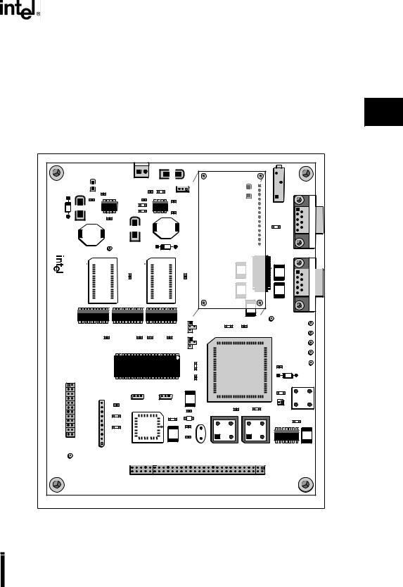
This chapter describes the Intel 186 EC/EB Evaluation Board kit, and provides setup instructions. Figure 2-1 shows the 80x186 EB Evaluation Board layout, and Figure 2-2 shows the EC board 2 layout. Refer to these figures when you are following the instructions in this chapter for setting
up your evaluation board.
|
C32 |
|
|
|
J2 |
|
|
|
|
|
|
|
|
|
C12 |
|
|
|
|
|
|
|
|
|
|
|
|
|
J1 |
|
R2 |
|
|
|
|
|
|
|
|
|
|
|
|
|
|
|
|
|
|
|
|
|
|
|
|
|
|
|
|
|
|
|
|
|
|
|
|
|
|
|
|
|
+5V GND |
|
|
5V/3V Select |
|
|
|
|
|
|
|
|
|
|
|
|
|
|
|
|
|||||||||
|
|
|
|
|
|
|
C22 |
R9 |
|
|
|
|
|
|
|
|
|
|
|
|
|
|
|
|
|||||||||
|
C33 |
|
|
|
|
|
|
|
|
|
|
E1 |
|
|
|
|
|
|
|
|
|
C5 |
|
|
|
|
|
|
P1 |
||||
|
|
C26 |
|
|
|
|
|
|
|
|
A B C |
|
|
|
|
|
|
|
|
|
|
|
|
|
|
|
|||||||
|
C31 |
|
|
|
C25 |
|
|
|
|
|
|
|
|
|
|
|
|
|
|
|
|
|
|
|
|
|
|
|
|
|
|
|
|
|
|
|
|
|
|
|
|
|
|
|
|
C20 |
|
|
|
|
|
|
|
|
|
|
|
|
|
|
|
|
|
|
|||
|
|
|
|
U11 R10 |
|
|
|
|
|
|
|
|
|
|
|
|
|
|
|
|
|
|
|
|
|
|
|
|
|
||||
D3 |
|
|
|
|
|
|
|
|
U7 |
|
|
|
|
|
|
|
|
|
|
|
|
|
|
|
|
|
|
|
PC |
|
|||
|
|
|
|
R11 |
|
|
|
|
|
|
|
C21 |
|
|
|
|
|
|
|
|
|
|
|
|
|
|
|
|
|
||||
|
|
|
|
C28 |
|
|
|
|
|
|
|
|
|
|
|
|
|
|
|
|
|
|
|
|
|
|
|
|
|
|
R3 |
Interface |
|
|
|
|
|
|
|
|
|
|
|
|
|
|
|
L2 |
|
|
|
|
|
|
|
|
|
|
|
|
|
|
|
|
|
||
|
L3 |
|
|
|
|
|
|
|
|
|
|
|
|
|
|
|
|
|
|
|
|
|
|
|
|
|
|
|
|
|
|
||
|
|
GND |
|
TP7 |
C27 |
|
|
|
|
|
|
|
D2 |
|
|
|
|
|
|
|
|
|
|
|
|
|
|
|
|
|
|
|
|
|
|
|
|
|
|
|
|
|
|
|
|
|
|
|
|
|
|
|
|
|
|
|
|
|
U2 |
|
|
|
|
||||
|
|
|
|
|
|
|
|
|
|
|
|
|
|
|
|
|
|
|
|
|
|
|
|
|
|
|
|
|
|
P2 |
|||
|
|
|
|
|
|
|
|
|
|
|
|
|
|
|
|
|
|
|
|
|
|
|
|
|
|
|
|
|
|
|
C2 |
|
|
|
|
|
|
U13 |
|
|
|
|
|
|
|
|
U8 |
|
|
|
|
|
|
|
|
|
|
C7 |
|
|
|
|
|
|
DCE |
|
|
|
|
|
|
|
|
|
|
|
|
|
|
|
|
|
|
|
|
|
|
|
|
|
|
|
|
|
|
|
|
|
|
||
80X186EB |
|
|
|
|
C29 |
|
|
|
|
|
|
|
|
C13 |
|
|
|
|
|
|
|
|
C8 |
|
|
|
|
|
|
C3 |
Connector |
|
|
5V / 3V EVAL |
|
|
|
|
|
|
|
|
|
|
|
|
|
PROT |
D E3 D E2 WRT |
|
|
|
|
|
|
|
|
C6 |
|
|
|
|
TP6 GND |
|
TP3 TP2 TP1 |
||
U14 |
|
|
|
U12 |
|
|
|
|
U6 |
|
|
|
C B A C B A |
|
|
|
|
R6 |
|
|
C9 |
|
|
|
|
|
|||||||
|
|
|
|
|
|
|
|
|
|
|
|
|
|
|
|
|
|
|
|
|
|
||||||||||||
|
C34 |
|
C24 C23 |
C14 |
|
|
U4 |
|
|
|
|
|
|
|
|
|
|
|
|||||||||||||||
|
|
|
|
|
|
|
|
|
|
|
|
|
|
|
|
|
|||||||||||||||||
|
|
|
|
|
|
|
|
|
|
|
|
|
|
|
|
|
|
|
|
|
|
|
|
|
|||||||||
|
|
|
|
|
|
|
|
|
|
|
|
|
|
|
|
V |
|
|
|
|
|
|
|
|
|
|
|
|
|
|
|
TP5 TP4 |
|
|
|
|
|
|
|
|
|
|
|
|
|
|
|
|
PP SELECT |
|
R7 |
|
|
|
|
|
|
|
|
|
|
|
|
C4 |
|||
|
JP2 |
|
|
|
|
|
|
|
|
|
|
|
|
U9 |
|
|
C11 |
|
|
|
|
|
|
|
|
|
|
|
|
|
|
D1 |
|
VCC |
|
|
|
|
|
|
|
|
|
|
|
|
|
|
|
|
|
|
|
|
|
|
|
|
|
|
|
|
S1 |
||||
VCC |
|
|
|
186/188 |
|
|
FLASH |
|
|
C15 |
|
|
|
|
|
|
|
|
|
|
|
|
|
R4 |
|
||||||||
T1OUT |
T0IN |
|
|
|
SELECT |
|
|
PWRDN |
|
|
|
|
|
|
|
|
|
|
|
|
|
|
|
|
|
||||||||
T0OUT |
T1IN |
|
|
|
|
|
|
|
|
|
|
|
|
|
|
|
|
|
|
|
|
|
|
|
|
|
|
||||||
|
|
|
|
|
E3 |
|
|
|
E4 |
|
|
|
|
|
|
|
|
|
|
|
|
|
|
|
|
|
|
|
|
||||
GND |
GND |
|
|
|
|
|
|
|
|
|
|
|
|
|
|
|
|
|
|
|
|
|
|
|
|
|
|
|
|
||||
P2.2 |
INT0 |
|
|
|
A B C |
|
|
A B C |
|
|
|
|
|
|
|
|
|
|
|
|
|
|
|
|
|
|
|
|
|
||||
P2.3 |
INT1 |
|
|
C30 |
|
|
|
|
|
U10 |
|
|
|
|
|
|
C16 |
|
|
|
|
C10 |
|
|
|
|
|
R5 |
Q1 |
|
|
||
BCLK0 |
INT2 |
|
|
|
|
|
|
|
R8 |
|
|
|
|
|
|
|
|
|
|
|
|
|
|
|
|||||||||
P2.6 |
INT3 |
|
|
|
|
|
|
|
|
|
|
|
|
|
L1 |
|
|
|
|
|
|
|
|
|
|
|
|
|
|
R1 |
|||
P2.7 |
INT4 |
|
|
R12 |
|
|
|
|
|
|
|
|
|
|
|
|
|
|
|
|
|
|
|
|
|
|
|
|
|
|
|||
|
|
|
|
|
|
|
|
|
|
|
|
|
|
|
|
|
|
|
|
|
|
|
|
|
|
|
|
|
|
|
|||
GND |
GND |
|
|
|
|
|
|
|
|
|
|
|
|
|
|
|
|
|
|
|
|
|
|
|
|
|
|
|
|
|
|
|
|
+5V |
GCS6# |
|
|
R13 |
|
|
|
|
|
|
|
|
|
C17 |
|
|
|
|
|
|
|
|
|
|
|
|
|
|
|
|
|
||
+12V |
GCS7# |
|
|
|
|
|
|
|
|
|
|
|
|
|
|
|
|
|
|
|
|
|
|
|
|
|
|
|
|
||||
|
|
|
|
|
|
|
|
|
|
|
|
|
|
|
|
|
|
|
|
|
|
|
|
|
|
|
|
|
|
|
|
||
|
|
|
|
|
|
|
|
|
|
|
C19 |
C18 |
|
Y1 |
U5 |
|
|
|
|
U3 |
|
|
|
|
|
|
|
||||||
|
|
RP1 |
|
|
|
|
RESOUT |
|
|
|
|
|
|
|
|
|
|
|
|
|
|
|
|
U1 |
C1 |
||||||||
GND |
TP8 |
|
|
R#-DT GND |
DEN# |
BHE# |
LA19 RD# WR# |
LA18 |
LA17 |
LA16 |
GND |
LA15 |
LA14 |
LA13 |
LA12 |
LA11 |
LA10 |
LA9 |
LA8 |
LA7 GND |
LA6 |
LA5 |
LA3 LA4 |
LA2 |
LA1 |
LA0 |
V |
|
|
|
|||
|
|
CC |
JP1 |
|
|
||||||||||||||||||||||||||||
|
|
|
|
|
CLKOUT GND |
+5V |
+12V |
GCS5# |
ALE LOCK# NMI |
READY |
HOLD |
HLDA |
GND |
AD15 |
AD14 |
AD13 |
AD12 |
AD11 |
AD10 |
AD9 |
AD8 |
AD7 GND |
AD6 |
AD5 |
AD3 AD4 |
AD2 |
AD1 |
AD0 |
V |
|
|
||
|
|
|
|
|
|
|
|
||||||||||||||||||||||||||
|
|
|
|
|
CC |
|
|
|
|||||||||||||||||||||||||
|
|
|
|
|
|
|
|
|
|
|
|
|
|
|
|
|
|
|
|
|
|
|
|
|
|
|
|
|
|
|
|
|
A5289-01 |
Figure 2-1. Intel 186 EB Evaluation Board Layout
2-1

INTEL 186 EB/EC EVALUATION BOARD USER’S MANUAL
|
C32 |
|
|
J2 |
|
|
|
|
|
|
|
|
|
C19 |
|
|
|
|
|
|
|
|
|
|
|
|
|
J1 |
R2 |
|
|
|
|
|
+5V GND |
|
|
|
|
|
|
|
|
|
|
|
|
|
|
|
|
|
|
|
|
|
|
|
|||||
|
|
|
|
|
5V/3V Select |
|
|
|
|
|
|
|
|
|
|
|
|
|
|
|
|||||||||||
|
|
|
|
|
|
|
C21 R11 |
|
|
|
|
|
|
|
|
|
|
|
|
|
|
|
|||||||||
|
C33 |
|
C30 |
|
|
|
|
|
|
|
|
A B C |
E1 |
|
|
|
|
|
|
|
|
C8 |
|
|
|
|
P1 |
|
|||
|
C31 |
|
|
|
|
|
|
|
|
|
|
|
|
|
|
|
|
|
|
|
|
|
|
|
|
||||||
|
|
|
|
|
|
|
|
|
|
|
|
|
|
|
|
|
|
|
|
|
|
|
|
|
|
|
|
|
|
|
|
|
|
|
|
C24 |
|
|
|
|
|
|
C20 |
|
|
|
|
|
|
|
|
|
|
|
|
|
|
|
|
|
|||
D3 |
|
|
U11 R12 |
|
|
|
|
|
U6 |
|
|
|
|
|
|
|
|
|
|
|
|
|
|
|
|
|
|
PC |
|
||
|
|
|
R13 |
|
|
|
|
|
|
|
C22 |
|
|
|
|
|
|
|
|
|
|
|
|
|
|
|
|
||||
|
|
|
C26 |
|
|
|
|
|
|
|
|
|
|
|
|
|
|
|
|
|
|
|
|
|
|
|
|
|
|
Interface |
|
|
L3 |
|
|
|
|
|
|
|
|
|
|
|
L2 |
|
|
|
|
|
|
|
|
|
|
|
|
|
|
|
R3 |
|
|
|
|
GND |
TP7 |
C25 |
|
|
|
|
|
|
|
|
|
|
|
|
|
|
|
|
|
|
|
|
|
U2 |
|
|
|
||
|
|
|
|
|
|
|
|
|
|
|
|
|
|
|
|
|
|
|
|
|
|
|
|
|
|
|
P2 |
|
|||
|
|
|
|
|
|
|
|
|
|
|
|
|
|
|
|
|
|
|
|
|
|
|
|
|
|
|
|
|
C2 |
|
|
|
|
|
U13 |
|
|
|
|
|
U7 |
|
|
|
|
|
|
|
|
|
|
|
C11 |
|
|
|
|
|
|
DCE |
|
||
|
|
|
|
|
|
|
|
|
|
|
|
|
|
|
|
|
|
|
|
|
|
|
|
|
|
|
|
|
|
||
/ 3V EVAL 80X186EC |
|
|
|
C27 |
|
|
|
|
|
|
C15 |
PROT WRT C B A |
|
|
|
|
|
|
|
|
|
|
|
|
|
|
C3 |
Conntector |
|
||
|
|
|
|
|
|
|
|
|
D E2 |
|
|
|
|
GND |
TP6 |
|
C10 |
|
|
|
|
TP1 |
|||||||||
U14 |
|
|
|
|
|
|
U8 |
|
U5 |
|
|
U3C12 |
|
|
|
|
C4 |
||||||||||||||
5V |
|
|
U12 |
|
|
|
|
|
|
|
|
D E3 |
|
|
|
|
|
|
|
|
|
|
|
|
|
C9 |
L1 |
TP4 TP3 TP2 |
|||
|
|
|
|
|
|
|
|
|
|
|
|
|
|
|
|
|
|
|
|
|
|
|
|
|
|
|
C5 |
||||
|
|
|
|
|
|
|
|
|
|
|
|
|
|
|
|
|
|
|
|
|
|
|
|
|
|
|
|
||||
|
|
|
C28 |
C23 |
|
|
|
|
V |
|
|
|
|
|
|
|
|
|
|
|
|
|
|
|
|||||||
|
|
|
|
|
|
|
|
|
|
|
|
|
|
|
|
|
|
|
|
|
|
|
|
|
|
|
|||||
|
C34 |
|
|
|
|
|
|
C16 |
|
PP CBA |
|
|
|
|
|
|
|
|
|
|
|
|
|
|
Y1 |
||||||
|
|
|
|
|
|
|
|
|
|
|
|
|
|
C13 |
|
R8 |
R7 |
|
|||||||||||||
|
|
|
|
|
|
|
|
|
|
|
|
|
SELECT |
|
|
|
|
|
|
|
|
C6 |
TP5 |
||||||||
T0IN |
T1OUT |
|
|
|
|
|
|
|
|
|
|
|
|
|
|
|
|
|
|
|
|
|
|
|
|
|
|
||||
T1IN |
T0OUT |
RP1 |
|
|
|
|
|
|
|
|
|
|
|
|
|
|
|
|
|
|
|
|
|
|
|
|
U4 |
D1 |
|||
VCC |
VCC |
|
|
|
|
|
|
|
|
|
|
|
|
|
|
|
|
|
|
|
|
|
|
|
|
|
|||||
JP2 |
P3.0 |
|
|
|
|
|
|
|
|
U9 |
|
|
|
|
|
|
|
|
|
|
|
|
|
|
|
|
|
||||
INT0 |
|
|
|
|
|
|
|
|
|
|
R9 |
|
|
|
|
|
|
|
|
|
|
|
|
|
|
|
|
||||
INT1 |
P3.1 |
|
|
|
|
|
|
|
|
|
|
|
|
|
|
|
|
|
|
|
|
|
|
|
|
|
R4 |
|
|
||
|
|
186/188 |
|
|
FLASH |
|
|
|
|
|
|
|
|
|
|
|
|
|
|
|
|
|
|
||||||||
INT2 |
P3.2 |
|
|
|
|
|
|
|
|
|
|
|
|
|
|
|
|
|
|
|
|
Q1 |
|
|
|||||||
INT3 |
P3.3 |
|
|
SELECT |
|
PWRDN |
|
|
|
|
|
|
|
|
|
|
|
|
|
|
|
|
|
||||||||
INT4 |
P3.4 |
|
|
|
|
|
E5 |
|
|
|
|
E4 |
|
|
|
|
|
|
|
|
|
|
|
|
|
|
|
|
|
|
|
INT5 |
P3.5 |
|
C29 |
|
|
|
A B C |
|
|
|
|
|
|
|
|
|
|
|
|
|
|
|
C7 |
|
S1 |
||||||
|
A B C |
|
|
|
|
|
|
|
|
|
|
|
|
|
|
|
|
|
|
||||||||||||
INT6 |
WDTOUT# |
|
|
|
|
|
|
|
|
|
|
|
|
|
|
|
|
|
|
R5 |
|
||||||||||
|
|
|
C17 |
|
|
|
|
|
|
|
|
|
|
|
|
|
|
||||||||||||||
INT7 |
GND |
|
|
|
|
|
|
|
U10 |
|
|
|
|
|
|
|
|
|
|
|
|
|
|
|
|
|
|
|
R1 |
||
INTA# |
BCLK0 |
|
|
|
|
|
|
|
|
|
|
|
|
R10 |
|
|
|
|
|
|
|
|
|
|
|
|
R6 |
||||
GND |
P2.3 |
|
|
|
|
|
|
|
|
|
|
|
|
|
|
|
|
|
|
|
|
|
|
|
|
|
|
|
|
|
|
DRQ0 |
RXD1 |
|
|
|
|
|
|
|
|
|
|
|
|
|
|
|
|
|
|
|
|
|
|
|
|
|
|
|
|
|
|
DRQ1 |
TXD1 |
|
|
|
|
|
|
|
|
|
|
|
|
|
|
|
|
|
|
|
|
|
|
|
|
|
|
|
|
|
|
DRQ2 |
P2.6 |
|
|
|
|
|
|
|
|
|
|
|
|
|
|
|
|
|
|
|
|
|
|
|
|
|
|
|
|
|
|
DRQ3 |
CTS1# |
|
|
|
|
|
|
|
|
|
|
|
|
|
|
|
|
|
|
|
|
|
|
|
|
|
|
|
|
|
|
GND |
GND |
|
|
|
|
|
|
|
|
|
|
C18 |
|
|
|
|
|
|
|
C14 |
|
|
|
|
|
U1 |
C1 |
||||
GCS6# |
+5V |
|
|
|
|
|
|
|
|
|
|
|
|
|
|
|
|
|
|
|
|
|
|
|
|
|
|
|
|||
GCS7# |
+12V |
|
|
|
|
|
|
|
|
|
|
|
|
|
|
|
|
|
|
|
|
|
|
|
|
|
|
|
|
|
|
GND |
TP8 |
|
|
GND |
R#-DT |
DEN# |
RESOUT |
BHE# |
LA19 RD# WR# |
LA18 |
LA17 |
LA16 |
GND |
LA15 |
LA14 |
LA13 |
LA12 |
LA11 |
LA10 |
LA8 LA9 |
LA7 GND |
LA6 |
LA5 |
LA4 |
LA2 LA3 |
LA1 |
LA0 |
V |
|
|
|
|
|
CC |
|
|
|||||||||||||||||||||||||||
|
|
|
|
|
|
|
|
|
|
|
|
|
|
|
|
|
|
|
|
|
|
|
|
|
|
|
|
|
JP1 |
|
|
|
|
|
|
GND |
CLKOUT |
+5V |
+12V |
GCS5# |
ALE LOCK# NMI |
READY |
HOLD |
HLDA |
GND |
AD15 |
AD14 |
AD13 |
AD12 |
AD11 |
AD10 |
AD8 AD9 |
AD7 GND |
AD6 |
AD5 |
AD4 |
AD3 |
AD2 |
AD1 |
AD0 |
V |
|
|
|
|
|
|
CC |
|
|
|||||||||||||||||||||||||
|
|
|
|
|
|
|
|
|
|
|
|
|
|
|
|
|
|
|
|
|
|
|
|
|
|
|
|
|
|
|
A5288-01 |
Figure 2-2. Intel 186 EC Evaluation Board Layout
2-2

GETTING STARTED
2.1SYSTEM REQUIREMENTS
•IBM* PC AT, XT or BIOS-compatible computer host system (interfaces via COM1 or COM2 at 9600 baud).
•5 V power supply (the connector housing and contact pins are included in the kit).
2
2.2WHAT’S IN YOUR KIT
Evaluation Board |
Your kit includes a board with either a 3.3 volt, 16 MHz |
|
80L186EB or 80L186EC microprocessor installed. Separately |
|
packaged components included with the board are 5 VDC ver- |
|
sions of the microprocessor and SRAM for conversion to a |
|
5 VDC evaluation platform. |
Monitor Program |
The Embedded Controller Monitor (ECM) program supports |
|
basic software and hardware evaluation and basic debug facilities |
|
(LOAD, GO, STEP, etc.) on the evaluation board. The ECM con- |
|
sists of two programs: RISM-186 executes in the evaluation board |
|
and ECM-86 executes in an IBM PC or BIOS-compatible com- |
|
puter, called the host PC. These two programs communicate |
|
through an asynchronous serial channel using a binary protocol |
|
defined specifically for this application. |
|
The source code for the monitor software is provided on a diskette |
|
included in your kit; this allows you to update the software for |
|
various operating conditions in your target application. |
Contents on Disk |
In addition to Flash downloading software, a diskette provided in |
|
the kit contains schematics, a pld file for the programmable logic |
|
device used on the board, and a sample assembly file for working |
|
the with LCD display. Compiler software is not included in the |
|
kit. |
Software Development |
The kit provides a software development kit, which includes a |
Kit |
software debugger, locator, and sample code. |
Flash Loading |
Users can download application programs to the on-board Flash |
Utility |
memory for execution. The Flash loading utility is contained on a |
|
diskette, and a separate manual, the CQI Flash Loader User’s |
|
Manual, provides instructions for using this utility. |
Serial Cable |
A serial cable is provided to connect the evaluation board to the |
|
host PC. |
2-3

INTEL 186 EB/EC EVALUATION BOARD USER’S MANUAL
2.3VIEWING THE BOARD SCHEMATICS
The schematics provided on the diskette are in the Adobe* Acrobat .pdf format. You can view and print the schematics using the Acrobat Reader. The Reader is available at no charge from the Intel World Wide Web site (http://www.intel.com/) or from the Adobe site (http://www.adobe.com/).
2.4SETTING UP THE EVALUATION BOARD AND THE HOST PC
This section tells you how to set up the board for use with a host PC. This section assumes you won’t be using some of the advanced features of the board when you first power it up. For additional options, such as selecting 80188 evaluation mode, refer to Chapter 3, “Hardware Overview.”
1.Make sure you are in a static-free environment before removing any components from their anti-static packaging. The evaluation board is susceptible to electro-static discharge damage; such damage may cause product failure or unpredictable operation.
2.Inspect the contents of your kit. Make sure that all items are included. Check for damage that may have occurred during shipment. Contact your sales representative if any items are missing or damaged.
CAUTION: Many of the connectors on the evaluation board provide power through nonstandard pins. Connecting the wrong cable or reversing the cable can damage the evaluation board and may damage the device being connected. Use extreme caution when preparing to connect cables to this product.
3.Connect the power supply. The Intel 186 EC/EB Evaluation Board operates from a
5 VDC ± 10% power supply plugged into the J2 power connector (see Figures 2-1 and 2-2). This 5 volt signal is stepped down to 3.3 volts on the board. The connector housing and contact pins provided in your kit match the power supply to the J2 connector.
To select 5 V, place a jumper on pins B and C of jumper E1. To select 3 V, place a jumper on pins A and B of jumper E1. See Figures 2-1 and 2-2 for jumper locations.
All devices on the board operate at both 3.3 volts and 5.0 volts (except the LCD display, which is hardwired to 5 volts). This option allows comparison of current consumption when running code at either voltage. Separately packaged 5 V versions of the 80C186 processor and SRAM must be installed on the board for 5 V operation.
2-4
GETTING STARTED
4.Apply power to the host PC and the evaluation board.
When power is applied to the board, the message “i186 Ex 3V/5V EV” should appear across the LCD display. This message indicates board initialization is complete. If the message does not appear, press the reset button (S1).
Connect one end of the standard 9-pin AT-type serial connector to header P1 on the evaluation board. Connect the other end to the COM1 port of the host computer. (You can 2 use COM2 if you need to, but you’ll have to specify COM2 when you run the Monitor Software.) The PC and board communicate at 9600 baud.
After connection to the PC, the processor may appear to be held in the reset state. The reason this occurs is that one of the host signals is used to reset the board. This signal may be active prior to invoking the ECM86 host software on the PC. The PC and board communicate at 9600 baud.
5.Insert the ECM-86 floppy disk provided with your kit in the floppy drive on the host PC. You can run the ECM86 program directly from the diskette or copy the contents of the diskette to your hard drive.
6.At the DOS prompt, change to the floppy disk drive (or to the directory to which you copied the files in the previous step) and enter this command:
ECM86
After a moment, the PC should display the ECM86 monitor screen.
Complete information on using the monitor software is located in Chapters 4 and 5.
2-5

3
Hardware Overview

HARDWARE OVERVIEW
CHAPTER 3
HARDWARE OVERVIEW
The evaluation board comes with a 16 MHz 80L186 EB or EC processor, 512 Kbytes of Flash (containing the iRISM-186 monitor and a Flash loader utility in the boot block), and 256 Kbytes of SRAM. The expansion connector (JP1) supports up to 1 Mbyte of external memory and
64 Kbytes of external I/O. Refer to Figures 2-1 and 2-2 for the exact locations of connectors, 3 jumpers and headers listed in this chapter.
The board utilizes the high peripheral integration of the 186 product family. The programmable chip-selects support on-board memory, expansion memory, and the LCD interface. The timer/counter unit controls timing for LCD display accesses. The serial control unit communicates with the host PC through the iECM-86 software and the Flash loader host software. Finally, the I/O port unit controls on-board power management functions (enable/disable serial drivers and +12 volts).
Other on-chip peripherals are made available for hardware expansion via the JP1, JP2, and P2 connectors. The following sections describe in detail the specific devices used on the board.
3.1JUMPER SUMMARY
Table 3-1. 80x186EB/EC Evaluation Board Jumper Settings
Jumper |
Name |
Description |
Options |
|
|
|
|
E1 |
5 V/3 V Select |
Selects voltage (5 V or 3.3 V) that |
A-B = 3.3 V† |
|
|
will be present on VCC power plane. |
B-C = 5 V |
|
|
|
|
E2 |
LA19/WRT PROT |
Selects options for Flash WP# pin. |
A-B = Write protect boot block† |
|
|
Includes option to make LA19 |
B-C = Unlock boot block |
|
|
available to Flash pin 2 for upgrading |
|
|
|
B-D = Add LA19 for 8- MBIT |
|
|
|
to 8-MBIT component |
|
|
|
Flash |
|
|
|
(PA28F800BV). |
|
|
|
|
|
|
|
|
|
E3 |
VPP Select |
Selects 5 V or 12 V programming |
A-B = Total WRT protect† |
|
|
voltage, as well as GND to remove |
B-C = 12 V program voltage |
|
|
all program and erase capabilities. |
|
|
|
B-D = 5 V program voltage |
|
|
|
|
|
|
|
|
|
E4 |
Flash Powerdown |
Selects options for Flash RP# pin. |
A-B = Normal† |
|
Select |
For normal operation, SW-RES# is |
B-C = Program boot block |
|
|
selected. To unlock boot block |
override |
|
|
(regardless of WP#), 12 V is |
|
|
|
|
|
|
|
selected. |
|
|
|
|
|
E5 |
186/188 Select |
Jumper for appropriate processor |
A-B = 188 processor installed |
|
|
type. |
B-C = 186 processor installed† |
† Default setting
3-1

INTEL 186 EB/EC EVALUATION BOARD USER’S MANUAL
3.2MICROPROCESSOR
The core of the evaluation board is the 80x186 microprocessor. This processor operates at 3.3 volts up to 16 MHz in this board. Alternatively, the board can be configured to run at 5 volts up to 33 MHz. To vary the CPU clock speed, an appropriate frequency value oscillator must be installed at location U3 on the EC board and at location U5 on the EB board. The oscillator operates at twice the frequency of the installed processor.
The 80x186 processor offers the following features:
•16-bit data bus
•1 Mbyte address space
•2 on-chip UARTs
•10 programmable chip-selects
•Interrupt control unit
•3 programmable timer/counters
•Power management unit
•32-bit watchdog timer (EC only)
•4 DMA channels (EC only)
The 8-bit bus version of the processor (80C188/80L188) may also be used in this board. To configure the board to operate with an 8-bit bus, jumper E5 must be in the A–B position. To configure the board to operate with a 16-bit bus, jumper E5 must be in the B–C position. Many of the processor’s on-chip peripherals can be accessed using the two expansion connectors on the board (JP1 and JP2).
NOTE
Because host communications use the on-chip serial ports, changing the operating frequency of the board requires the processor serial ports to be reconfigured. The RISM monitor source code is provided on a floppy diskette in your kit and is commented to indicate current register values.
3.2.1Packaging
The 80x186 EC is packaged in a 100 lead PQFP and socket and the 80x186 EB is packaged in an 84 lead PLCC package and socket. Adaptors are available from Applied Microsystems Corp.* and Emulation Technologies, Inc.* to allow for the connection of in-circuit emulators.
3-2

HARDWARE OVERVIEW
3.3MEMORY CONFIGURATION
The memory on the evaluation board can be divided into three types: Flash, SRAM, and expansion. Flash memory contains the Flash loader utility, located in the boot block boundary, and the RISM monitor program, beginning at F800:0000. Users can execute their test code from boot-up using the Flash loader utility. Refer to the CQI Flash Loader Reference Manual for instructions on programming the Flash memory. SRAM memory is used for the processor interrupt vector table, stack allocation, and RISM data variables, and as a possible destination for
user-written code downloaded on the host interface. Expansion memory can be accessed through 3 the expansion interface, if required.
Table 3-2 shows the logical memory map and Figure 3-1 shows the physical memory map of the evaluation board.
Table 3-2. Logical Memory Map
Memory Area |
Start (H) |
Stop (H) |
Size |
|
|
|
|
SRAM |
0000:0000 |
2000:0000 |
128 Kbytes |
|
|
|
|
Flash |
8000:0000 |
F000:FFFF |
512 Kbytes |
|
|
|
|
Flash Boot Block |
FC00:0000 |
F000:FFFF |
16 Kbytes |
|
|
|
|
Expansion |
4000:0000 |
8000:0000 |
256 Kbytes |
|
|
|
|
LCD (I/O) |
0000:0400 |
0000:0440 |
64 bytes |
|
|
|
|
3-3
Loading...