


Microcomputer Components
16-Bit CMOS Single-Chip Microcontroller
C167SR
Data Sheet 06.95 Advance Information
Edition 06.95
Published by Siemens AG, Bereich Halbleiter, MarketingKommunikation, Balanstraße 73, 81541 München
© Siemens AG 1995.
All Rights Reserved.
Attention please!
As far as patents or other rights of third parties are concerned, liability is only assumed for components, not for applications, processes and circuits implemented within components or assemblies.
The information describes the type of component and shall not be considered as assured characteristics.
Terms of delivery and rights to change design reserved.
For questions on technology, delivery and prices please contact the Semiconductor Group Offices in Germany or the Siemens Companies and Representatives worldwide (see address list).
Due to technical requirements components may contain dangerous substances. For information on the types in question please contact your nearest Siemens Office, Semiconductor Group.
Siemens AG is an approved CECC manufacturer.
Packing
Please use the recycling operators known to you. We can also help you – get in touch with your nearest sales office. By agreement we will take packing material back, if it is sorted. You must bear the costs of transport.
For packing material that is returned to us unsorted or which we are not obliged to accept, we shall have to invoice you for any costs incurred.
Components used in life-support devices or systems must be expressly authorized for such purpose!
Critical components1 of the Semiconductor Group of Siemens AG, may only be used in life-support devices or systems2 with the express written approval of the Semiconductor Group of Siemens AG.
1A critical component is a component used in a life-support device or system whose failure can reasonably be expected to cause the failure of that life-support device or system, or to affect its safety or effectiveness of that device or system.
2Life support devices or systems are intended (a) to be implanted in the human body, or (b) to support and/or maintain and sustain human life. If they fail, it is reasonable to assume that the health of the user may be endangered.
Ausgabe 06.95
Herausgegeben von Siemens AG, Bereich Halbleiter, MarketingKommunikation, Balanstraße 73, 81541 München
© Siemens AG 1995. Alle Rechte vorbehalten.
Wichtige Hinweise!
Gewähr für die Freiheit von Rechten Dritter leisten wir nur für Bauelemente selbst, nicht für Anwendungen, Verfahren und für die in Bauelementen oder Baugruppen realisierten Schaltungen.
Mit den Angaben werden die Bauelemente spezifiziert, nicht Eigenschaften zugesichert.
Liefermöglichkeiten und technische Änderungen vorbehalten.
Fragen über Technik, Preise und Liefermöglichkeiten richten Sie bitte an den Ihnen nächstgelegenen Vertrieb Halbleiter in Deutschland oder an unsere Landesgesellschaften im Ausland.
Bauelemente können aufgrund technischer Erfordernisse Gefahrstoffe enthalten. Auskünfte darüber bitten wir unter Angabe des betreffenden Typs ebenfalls über den Vertrieb Halbleiter einzuholen.
Die Siemens AG ist ein Hersteller von CECCqualifizierten Produkten.
Verpackung
Bitte benutzen Sie die Ihnen bekannten Verwerter. Wir helfen Ihnen auch weiter – wenden Sie sich an Ihren für Sie zuständigen Vertrieb Halbleiter. Nach Rücksprache nehmen wir Verpackungsmaterial sortiert zurück. Die Transportkosten müssen Sie tragen.
Für Verpackungsmaterial, das unsortiert an uns zurückgeliefert wird oder für das wir keine Rücknahmepflicht haben, müssen wir Ihnen die anfallenden Kosten in Rechnung stellen.
Bausteine in lebenserhaltenden Geräten oder Systemen müssen ausdrücklich dafür zugelassen sein!
Kritische Bauelemente1 des Bereichs Halbleiter der Siemens AG dürfen nur mit ausdrücklicher schriftlicher Genehmigung des Bereichs Halbleiter der Siemens AG in lebenserhaltenden Geräten oder Systemen2 eingesetzt werden.
1Ein kritisches Bauelement ist ein in einem lebenserhaltenden Gerät oder System eingesetztes Bauelement, bei dessen Ausfall berechtigter Grund zur Annahme besteht, daß das lebenserhaltende Gerät oder System ausfällt bzw. dessen Sicherheit oder Wirksamkeit beeinträchtigt wird.
2Lebenserhaltende Geräte und Systeme sind (a) zur chirurgischen Einpflanzung in den menschlichen Körper gedacht, oder
(b) unterstützen bzw. erhalten das menschliche Leben. Sollten sie ausfallen, besteht berechtigter Grund zur Annahme, daß die Gesundheit des Anwenders gefährdet werden kann.

C167SR |
|
|
|
Revision History: |
Original Version: 06.95 (Advance Information) |
||
|
|
||
Previous Releases: |
Data Sheet C167 06.94 |
||
|
|
||
Page |
Subjects (changes compared to C167) |
||
|
|
||
31 |
Register PICON added |
||
|
|
||
36 |
VILS, VIHS, HYS, IOV added. |
||
|
|
||
36 |
RRST, IRWH, IRWL, IALEL, IALEH, IP6H, test cond. IOZx changed. |
||
|
|
||
37 |
IP6L, ICC, IID changed. |
||
|
|
||
37 |
ICC, IID typical values added |
||
|
|
||
39 |
ADC specification changed. |
||
|
|
||
41...43 |
PLL description added. |
||
|
|
||
44 |
External Clock Drive specification changed. |
||
|
|
||
46 |
t14, t15, t16, t17, t22, t39, t46 changed. |
||
47 |
t47 |
changed. |
|
52 |
t14, t15, t16, t17, t20, t21, t22 changed. |
||
|
|
||
53 |
t39, t46, t47, t55 changed. |
||
|
|
|
|
56, 57 |
t53 |
changed to t68. |
|
58 |
t36 |
changed. |
|
61 |
t63 |
changed. |
|

C16x-Family of |
C167SR |
High-Performance CMOS 16-Bit Microcontrollers
Advance Information
C167SR 16-Bit Microcontroller
●High Performance 16-bit CPU with 4-Stage Pipeline
●100 ns Instruction Cycle Time at 20 MHz CPU Clock
●500 ns Multiplication (16 × 16 bit), 1 µs Division (32 / 16 bit)
●Enhanced Boolean Bit Manipulation Facilities
●Additional Instructions to Support HLL and Operating Systems
●Register-Based Design with Multiple Variable Register Banks
●Single-Cycle Context Switching Support
●Clock Generation via on-chip PLL or via direct clock input
●Up to 16 MBytes Linear Address Space for Code and Data
●2 KBytes On-Chip Internal RAM (IRAM)
●2 KBytes On-Chip Extension RAM (XRAM)
●Programmable External Bus Characteristics for Different Address Ranges
●8-Bit or 16-Bit External Data Bus
●Multiplexed or Demultiplexed External Address/Data Buses
●Five Programmable Chip-Select Signals
●Holdand Hold-Acknowledge Bus Arbitration Support
●1024 Bytes On-Chip Special Function Register Area
●Idle and Power Down Modes
●8-Channel Interrupt-Driven Single-Cycle Data Transfer Facilities via Peripheral Event Controller (PEC)
●16-Priority-Level Interrupt System with 56 Sources, Sample-Rate down to 50 ns
●16-Channel 10-bit A/D Converter with 9.7 µs Conversion Time
●Two 16-Channel Capture/Compare Units
●4-Channel PWM Unit
●Two Multi-Functional General Purpose Timer Units with 5 Timers
●Two Serial Channels (Synchronous/Asynchronous and High-Speed-Synchronous)
●Programmable Watchdog Timer
●Up to 111 General Purpose I/O Lines, partly with Selectable Input Thresholds and Hysteresis
●Supported by a Wealth of Development Tools like C-Compilers, Macro-Assembler Packages, Emulators, Evaluation Boards, HLL-Debuggers, Simulators, Logic Analyzer Disassemblers, Programming Boards
●On-Chip Bootstrap Loader
●144-Pin MQFP Package (EIAJ)
This document describes the SAB-C167SR-LM, the SAF-C167SR-LM and the SAK-C167SR-LM. For simplicity all versions are referred to by the term C167SR throughout this document.
Semiconductor Group |
1 |
06.95 |

C167SR
C167SR |
|
|
|
Revision History: |
Original Version: 06.95 (Advance Information) |
||
|
|
||
Previous Releases: |
Data Sheet C167 06.94 |
||
|
|
||
Page |
Subjects (changes compared to C167) |
||
|
|
||
31 |
Register PICON added |
||
|
|
||
36 |
VILS, VIHS, HYS, IOV added. |
||
|
|
||
36 |
RRST, IRWH, IRWL, IALEL, IALEH, IP6H, test cond. IOZx changed. |
||
|
|
||
37 |
IP6L, ICC, IID changed. |
||
|
|
||
37 |
ICC, IID typical values added |
||
|
|
||
39 |
ADC specification changed. |
||
|
|
||
41...43 |
PLL description added. |
||
|
|
||
44 |
External Clock Drive specification changed. |
||
|
|
||
46 |
t14, t15, t16, t17, t22, t39, t46 changed. |
||
47 |
t47 |
changed. |
|
52 |
t14, t15, t16, t17, t20, t21, t22 changed. |
||
|
|
||
53 |
t39, t46, t47, t55 changed. |
||
|
|
|
|
56, 57 |
t53 |
changed to t68. |
|
58 |
t36 |
changed. |
|
61 |
t63 |
changed. |
|
Semiconductor Group |
2 |
C167SR
Introduction
The C167SR is a new derivative of the Siemens C16x Family of full featured single-chip CMOS microcontrollers. It combines high CPU performance (up to 10 million instructions per second) with high peripheral functionality and enhanced IO-capabilities. It also provides on-chip high-speed RAM and clock generation via PLL.
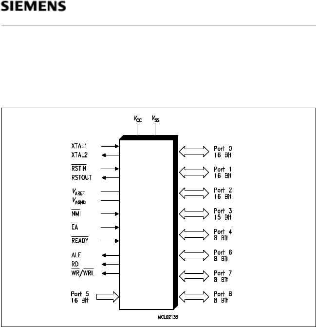
C167SR
Figure 1
Logic Symbol
Ordering Information
Type |
Ordering Code |
Package |
Function |
|
|
|
|
SAB-C167SR-LM |
Q67121-C952 |
P-MQFP-144-1 |
16-bit microcontroller with |
|
|
|
2 × 2 KByte RAM |
|
|
|
Temperature range 0 to + 70 ˚C |
|
|
|
|
SAF-C167SR-LM |
Q67121-C953 |
P-MQFP-144-1 |
16-bit microcontroller with |
|
|
|
2 × 2 KByte RAM |
|
|
|
Temperature range – 40 to + 85 ˚C |
|
|
|
|
SAK-C167SR-LM |
C |
P-MQFP-144-1 |
16-bit microcontroller with |
|
|
|
2 × 2 KByte RAM |
|
|
|
Temperature range – 40 to + 125 ˚C |
|
|
|
|
Semiconductor Group |
3 |
|
|

C167SR
Pin Configuration
(top view)
C167SR |
Figure 2
Semiconductor Group |
4 |

C167SR
Pin Definitions and Functions
Symbol |
Pin |
Input (I) |
Function |
|
|
|
|
|
|
|
|
Number |
Output (O) |
|
|
|
|
|
|
|
|
|
|
|
|
|||||||
P6.0 - |
1 - |
I/O |
Port 6 is an 8-bit bidirectional I/O port. It is bit-wise |
|||||||
P6.7 |
8 |
|
programmable for input or output via direction bits. For a pin |
|||||||
|
|
|
configured as input, the output driver is put into high- |
|||||||
|
|
|
impedance state. Port 6 outputs can be configured as push/ |
|||||||
|
|
|
pull or open drain drivers. |
|||||||
|
|
|
The following Port 6 pins also serve for alternate functions: |
|||||||
|
1 |
O |
P6.0 |
|
|
|
|
|
|
Chip Select 0 Output |
|
CS0 |
|||||||||
|
... |
... |
... |
... |
|
|
|
|
|
... |
|
5 |
O |
P6.4 |
|
|
|
|
|
Chip Select 4 Output |
|
|
CS4 |
|||||||||
|
6 |
I |
P6.5 |
|
|
|
|
External Master Hold Request Input |
||
|
HOLD |
|||||||||
|
7 |
O |
P6.6 |
|
|
|
Hold Acknowledge Output |
|||
|
HLDA |
|||||||||
|
8 |
O |
P6.7 |
|
|
Bus Request Output |
||||
|
BREQ |
|||||||||
|
|
|
|
|||||||
P8.0 - |
9 - |
I/O |
Port 8 is an 8-bit bidirectional I/O port. It is bit-wise |
|||||||
P8.7 |
16 |
|
programmable for input or output via direction bits. For a pin |
|||||||
|
|
|
configured as input, the output driver is put into high- |
|||||||
|
|
|
impedance state. Port 8 outputs can be configured as push/ |
|||||||
|
|
|
pull or open drain drivers. The input threshold of Port 8 is |
|||||||
|
|
|
selectable (TTL or special). |
|||||||
|
|
|
The following Port 8 pins also serve for alternate functions: |
|||||||
|
9 |
I/O |
P8.0 |
CC16IO |
CAPCOM2: CC16 Cap.-In/Comp.Out |
|||||
|
... |
... |
... |
... |
|
|
|
|
|
... |
|
16 |
I/O |
P8.7 |
CC23IO |
CAPCOM2: CC23 Cap.-In/Comp.Out |
|||||
|
|
|
|
|||||||
P7.0 - |
19 - |
I/O |
Port 7 is an 8-bit bidirectional I/O port. It is bit-wise |
|||||||
P7.7 |
26 |
|
programmable for input or output via direction bits. For a pin |
|||||||
|
|
|
configured as input, the output driver is put into high- |
|||||||
|
|
|
impedance state. Port 7 outputs can be configured as push/ |
|||||||
|
|
|
pull or open drain drivers. The input threshold of Port 7 is |
|||||||
|
|
|
selectable (TTL or special). |
|||||||
|
|
|
The following Port 7 pins also serve for alternate functions: |
|||||||
|
19 |
O |
P7.0 |
POUT0 |
PWM Channel 0 Output |
|||||
|
... |
... |
... |
... |
|
|
|
|
|
... |
|
22 |
O |
P7.3 |
POUT3 |
PWM Channel 3 Output |
|||||
|
23 |
I/O |
P7.4 |
CC28IO |
CAPCOM2: CC28 Cap.-In/Comp.Out |
|||||
|
... |
... |
... |
... |
|
|
|
|
|
... |
|
26 |
I/O |
P7.7 |
CC31IO |
CAPCOM2: CC31 Cap.-In/Comp.Out |
|||||
|
|
|
|
|
|
|
|
|
|
|
Semiconductor Group |
5 |

C167SR
Pin Definitions and Functions (cont’d)
Symbol |
Pin |
Input (I) |
Function |
|
|
|
Number |
Output (O) |
|
|
|
|
|
|
|
||
P5.0 - |
27 - 36 |
I |
Port 5 is a 16-bit input-only port with Schmitt-Trigger |
||
P5.15 |
39 - 44 |
I |
characteristics. The pins of Port 5 also serve as the (up to 16) |
||
|
|
|
analog input channels for the A/D converter, where P5.x |
||
|
|
|
equals ANx (Analog input channel x), or they serve as timer |
||
|
|
|
inputs: |
|
|
|
39 |
I |
P5.10 |
T6EUD |
GPT2 Timer T6 Ext.Up/Down Ctrl.Input |
|
40 |
I |
P5.11 |
T5EUD |
GPT2 Timer T5 Ext.Up/Down Ctrl.Input |
|
41 |
I |
P5.12 |
T6IN |
GPT2 Timer T6 Count Input |
|
42 |
I |
P5.13 |
T5IN |
GPT2 Timer T5 Count Input |
|
43 |
I |
P5.14 |
T4EUD |
GPT1 Timer T4 Ext.Up/Down Ctrl.Input |
|
44 |
I |
P5.15 |
T2EUD |
GPT1 Timer T2 Ext.Up/Down Ctrl.Input |
|
|
|
|
||
P2.0 - |
47 - 54 |
I/O |
Port 2 is a 16-bit bidirectional I/O port. It is bit-wise |
||
P2.15 |
57 - 64 |
|
programmable for input or output via direction bits. For a pin |
||
|
|
|
configured as input, the output driver is put into high- |
||
|
|
|
impedance state. Port 2 outputs can be configured as push/ |
||
|
|
|
pull or open drain drivers. The input threshold of Port 2 is |
||
|
|
|
selectable (TTL or special). |
||
|
|
|
The following Port 2 pins also serve for alternate functions: |
||
|
47 |
I/O |
P2.0 |
CC0IO |
CAPCOM: CC0 Cap.-In/Comp.Out |
|
... |
... |
... |
... |
... |
|
54 |
I/O |
P2.7 |
CC7IO |
CAPCOM: CC7 Cap.-In/Comp.Out |
|
57 |
I/O |
P2.8 |
CC8IO |
CAPCOM: CC8 Cap.-In/Comp.Out, |
|
|
I |
|
EX0IN |
Fast External Interrupt 0 Input |
|
... |
... |
... |
... |
... |
|
64 |
I/O |
P2.15 |
CC15IO |
CAPCOM: CC15 Cap.-In/Comp.Out, |
|
|
I |
|
EX7IN |
Fast External Interrupt 7 Input |
|
|
I |
|
T7IN |
CAPCOM2 Timer T7 Count Input |
|
|
|
|
|
|
Semiconductor Group |
6 |

C167SR
Pin Definitions and Functions (cont’d)
Symbol |
Pin |
Input (I) |
Function |
|
|
|
|
|
|
|
|
|
|
Number |
Output (O) |
|
|
|
|
|
|
|
|
|
|
|
|
||||||||
P3.0 - |
65 - 70, |
I/O |
Port 3 is a 15-bit (P3.14 is missing) bidirectional I/O port. It is |
||||||||
P3.13, |
73 - 80, |
I/O |
bit-wise programmable for input or output via direction bits. |
||||||||
P3.15 |
81 |
I/O |
For a pin configured as input, the output driver is put into high- |
||||||||
|
|
|
|
impedance state. Port 3 outputs can be configured as push/ |
|||||||
|
|
|
|
pull or open drain drivers. The input threshold of Port 3 is |
|||||||
|
|
|
|
selectable (TTL or special). |
|||||||
|
|
|
|
The following Port 3 pins also serve for alternate functions: |
|||||||
|
|
65 |
I |
P3.0 |
|
T0IN |
CAPCOM Timer T0 Count Input |
||||
|
|
66 |
O |
P3.1 |
|
T6OUT |
GPT2 Timer T6 Toggle Latch Output |
||||
|
|
67 |
I |
P3.2 |
|
CAPIN |
GPT2 Register CAPREL Capture Input |
||||
|
|
68 |
O |
P3.3 |
|
T3OUT |
GPT1 Timer T3 Toggle Latch Output |
||||
|
|
69 |
I |
P3.4 |
|
T3EUD |
GPT1 Timer T3 Ext.Up/Down Ctrl.Input |
||||
|
|
70 |
I |
P3.5 |
|
T4IN |
GPT1 Timer T4 Input for |
||||
|
|
|
|
|
|
|
|
|
Count/Gate/Reload/Capture |
||
|
|
73 |
I |
P3.6 |
|
T3IN |
GPT1 Timer T3 Count/Gate Input |
||||
|
|
74 |
I |
P3.7 |
|
T2IN |
GPT1 Timer T2 Input for |
||||
|
|
|
|
|
|
|
|
|
Count/Gate/Reload/Capture |
||
|
|
75 |
I/O |
P3.8 |
|
MRST |
SSC Master-Rec./Slave-Transmit I/O |
||||
|
|
76 |
I/O |
P3.9 |
|
MTSR |
SSC Master-Transmit/Slave-Rec. O/I |
||||
|
|
77 |
O |
P3.10 |
|
T×D0 |
ASC0 Clock/Data Output (Asyn./Syn.) |
||||
|
|
78 |
I/O |
P3.11 |
|
R×D0 |
ASC0 Data Input (Asyn.) or I/O (Syn.) |
||||
|
|
79 |
O |
P3.12 |
|
|
|
|
Ext. Memory High Byte Enable Signal, |
||
|
|
|
BHE |
||||||||
|
|
|
O |
|
|
|
|
Ext. Memory High Byte Write Strobe |
|||
|
|
|
|
WRH |
|||||||
|
|
80 |
I/O |
P3.13 |
|
SCLK |
SSC Master Clock Outp./Slave Cl. Inp. |
||||
|
|
81 |
O |
P3.15 |
|
CLKOUT |
System Clock Output (=CPU Clock) |
||||
|
|
|
|
||||||||
P4.0 - |
85 - 92 |
I/O |
Port 4 is an 8-bit bidirectional I/O port. It is bit-wise |
||||||||
P4.7 |
|
|
programmable for input or output via direction bits. For a pin |
||||||||
|
|
|
|
configured as input, the output driver is put into high- |
|||||||
|
|
|
|
impedance state. |
|
|
|
||||
|
|
|
|
In case of an external bus configuration, Port 4 can be used to |
|||||||
|
|
|
|
output the segment address lines: |
|||||||
|
|
85 |
O |
P4.0 |
|
A16 |
Least Significant Segment Addr. Line |
||||
|
|
... |
... |
... |
... |
|
|
... |
|
|
|
|
|
89 |
O |
P4.4 |
|
A20 |
Least Significant Segment Addr. Line |
||||
|
|
... |
... |
.. |
: |
|
|
: |
|
|
|
|
|
92 |
O |
P4.7 |
|
A23 |
Most Significant Segment Addr. Line |
||||
|
|
|
|
|
|
|
|||||
|
|
95 |
O |
External Memory Read Strobe. |
|
is activated for every |
|||||
RD |
RD |
||||||||||
|
|
|
|
external instruction or data read access. |
|||||||
|
|
|
|
|
|
|
|
|
|
|
|
Semiconductor Group |
7 |
C167SR
Pin Definitions and Functions (cont’d)
Symbol |
Pin |
Input (I) |
Function |
|
|
|
|
|
||||
|
|
|
|
|
Number |
Output (O) |
|
|
|
|
|
|
|
|
|
|
|
|
|
|
|
|
|||
|
|
|
|
|
96 |
O |
External Memory Write Strobe. In |
|
-mode this pin is |
|||
WR/ |
WR |
|||||||||||
|
|
|
|
|
|
activated for every external data write access. In |
|
-mode |
||||
WRL |
|
|
WRL |
|||||||||
|
|
|
|
|
|
|
this pin is activated for low byte data write accesses on a 16- |
|||||
|
|
|
|
|
|
|
bit bus, and for every data write access on an 8-bit bus. See |
|||||
|
|
|
|
|
|
|
WRCFG in register SYSCON for mode selection. |
|||||
|
|
|
|
|
|
|||||||
|
|
|
|
|
97 |
I |
Ready Input. When the Ready function is enabled, a high |
|||||
READY |
||||||||||||
|
|
|
|
|
|
|
level at this pin during an external memory access will force |
|||||
|
|
|
|
|
|
|
the insertion of memory cycle time waitstates until the pin |
|||||
|
|
|
|
|
|
|
returns to a low level. |
|
|
|
|
|
|
|
|
|
|||||||||
ALE |
98 |
O |
Address Latch Enable Output. Can be used for latching the |
|||||||||
|
|
|
|
|
|
|
address into external memory or an address latch in the |
|||||
|
|
|
|
|
|
|
multiplexed bus modes. |
|
|
|
|
|
|
|
|
|
|
||||||||
|
|
99 |
I |
External Access Enable pin. A low level at this pin during and |
||||||||
EA |
||||||||||||
|
|
|
|
|
|
|
after Reset forces the C167SR to begin instruction execution |
|||||
|
|
|
|
|
|
|
out of external memory. A high level forces execution out of |
|||||
|
|
|
|
|
|
|
the internal ROM. ROMless versions must have this pin tied |
|||||
|
|
|
|
|
|
|
to ‘0’. |
|
|
|
|
|
|
|
|
|
|||||||||
PORT0: |
|
I/O |
PORT0 consists of the two 8-bit bidirectional I/O ports P0L |
|||||||||
P0L.0 - |
100 - |
|
and P0H. It is bit-wise programmable for input or output via |
|||||||||
P0L.7, |
107 |
|
direction bits. For a pin configured as input, the output driver |
|||||||||
P0H.0 - |
108, |
|
is put into high-impedance state. |
|
|
|
|
|||||
P0H.7 |
111-117 |
|
In case of an external bus configuration, PORT0 serves as |
|||||||||
|
|
|
|
|
|
|
the address (A) and address/data (AD) bus in multiplexed bus |
|||||
|
|
|
|
|
|
|
modes and as the data (D) bus in demultiplexed bus modes. |
|||||
|
|
|
|
|
|
|
Demultiplexed bus modes: |
|
|
|
|
|
|
|
|
|
|
|
|
Data Path Width: |
8-bit |
16-bit |
|||
|
|
|
|
|
|
|
P0L.0 - P0L.7: |
D0 - D7 |
D0 - D7 |
|||
|
|
|
|
|
|
|
P0H.0- P0H.7: |
I/O |
D8 - D15 |
|||
|
|
|
|
|
|
|
Multiplexed bus modes: |
|
|
|
|
|
|
|
|
|
|
|
|
Data Path Width: |
8-bit |
16-bit |
|||
|
|
|
|
|
|
|
P0L.0 - P0L.7: |
AD0 - AD7 |
AD0 - AD7 |
|||
|
|
|
|
|
|
|
P0H.0 - P0H.7: |
A8 - A15 |
AD8 - AD15 |
|||
|
|
|
|
|
|
|
|
|
|
|
|
|
Semiconductor Group |
8 |

C167SR
Pin Definitions and Functions (cont’d)
Symbol |
Pin |
Input (I) |
Function |
|
|
|
|
|
|
|
|
|
|||
|
|
|
|
Number |
Output (O) |
|
|
|
|
|
|
|
|
|
|
|
|
|
|
||||||||||||
PORT1: |
|
I/O |
PORT1 consists of the two 8-bit bidirectional I/O ports P1L |
||||||||||||
P1L.0 - |
118 - |
|
and P1H. It is bit-wise programmable for input or output via |
||||||||||||
P1L.7, |
125 |
|
direction bits. For a pin configured as input, the output driver |
||||||||||||
P1H.0 - |
128 - |
|
is put into high-impedance state. PORT1 is used as the 16-bit |
||||||||||||
P1H.7 |
135 |
|
address bus (A) in demultiplexed bus modes and also after |
||||||||||||
|
|
|
|
|
|
switching from a demultiplexed bus mode to a multiplexed |
|||||||||
|
|
|
|
|
|
bus mode. |
|
|
|
|
|
|
|
|
|
|
|
|
|
|
|
The following PORT1 pins also serve for alternate functions: |
|||||||||
|
|
|
|
132 |
I |
P1H.4 |
CC24IO |
CAPCOM2: CC24 Capture Input |
|||||||
|
|
|
|
133 |
I |
P1H.5 |
CC25IO |
CAPCOM2: CC25 Capture Input |
|||||||
|
|
|
|
134 |
I |
P1H.6 |
CC26IO |
CAPCOM2: CC26 Capture Input |
|||||||
|
|
|
|
135 |
I |
P1H.7 |
CC27IO |
CAPCOM2: CC27 Capture Input |
|||||||
|
|
|
|
|
|||||||||||
XTAL1 |
138 |
I |
XTAL1: |
Input to the oscillator amplifier and input to the |
|||||||||||
|
|
|
|
|
|
|
internal clock generator |
||||||||
XTAL2 |
137 |
O |
XTAL2: |
Output of the oscillator amplifier circuit. |
|||||||||||
|
|
|
|
|
|
To clock the device from an external source, drive XTAL1, |
|||||||||
|
|
|
|
|
|
while leaving XTAL2 unconnected. Minimum and maximum |
|||||||||
|
|
|
|
|
|
high/low and rise/fall times specified in the AC Characteristics |
|||||||||
|
|
|
|
|
|
must be observed. |
|
|
|
|
|
||||
|
|
|
|
|
|
|
|||||||||
|
|
|
|
140 |
I |
Reset Input with Schmitt-Trigger characteristics. A low level at |
|||||||||
RSTIN |
|||||||||||||||
|
|
|
|
|
|
this pin for a specified duration while the oscillator is running |
|||||||||
|
|
|
|
|
|
resets the C167SR. An internal pullup resistor permits power- |
|||||||||
|
|
|
|
|
|
on reset using only a capacitor connected to VSS. |
|||||||||
|
|
|
|
|
|
||||||||||
|
|
|
|
141 |
O |
Internal Reset Indication Output. This pin is set to a low level |
|||||||||
RSTOUT |
|||||||||||||||
|
|
|
|
|
|
when the part is executing either a hardware-, a softwareor a |
|||||||||
|
|
|
|
|
|
watchdog timer reset. |
|
remains low until the EINIT |
|||||||
|
|
|
|
|
|
RSTOUT |
|||||||||
|
|
|
|
|
|
(end of initialization) instruction is executed. |
|||||||||
|
|
|
|
|
|||||||||||
|
|
142 |
I |
Non-Maskable Interrupt Input. A high to low transition at this |
|||||||||||
NMI |
|||||||||||||||
|
|
|
|
|
|
pin causes the CPU to vector to the NMI trap routine. When |
|||||||||
|
|
|
|
|
|
the PWRDN (power down) instruction is executed, the |
|
|
|||||||
|
|
|
|
|
|
NMI |
|||||||||
|
|
|
|
|
|
pin must be low in order to force the C167SR to go into power |
|||||||||
|
|
|
|
|
|
down mode. If |
|
|
is high, when PWRDN is executed, the |
||||||
|
|
|
|
|
|
NMI |
|||||||||
|
|
|
|
|
|
part will continue to run in normal mode. |
|||||||||
|
|
|
|
|
|
If not used, pin |
|
should be pulled high externally. |
|||||||
|
|
|
|
|
|
NMI |
|||||||||
|
|
|
|
||||||||||||
VAREF |
37 |
– |
Reference voltage for the A/D converter. |
||||||||||||
VAGND |
38 |
– |
Reference ground for the A/D converter. |
||||||||||||
VPP |
84 |
– |
Flash programming voltage. This pin accepts the |
||||||||||||
|
|
|
|
|
|
programming voltage for flash versions of the C167SR. |
|||||||||
|
|
|
|
|
|
Note: This pin is not connected (NC) on non-flash versions. |
|||||||||
|
|
|
|
|
|
|
|
|
|
|
|
|
|
|
|
Semiconductor Group |
9 |

C167SR
Pin Definitions and Functions (cont’d)
Symbol |
Pin |
Input (I) |
Function |
|
Number |
Output (O) |
|
|
|
|
|
VCC |
17, 46, |
– |
Digital Supply Voltage: |
|
56, 72, |
|
+ 5 V during normal operation and idle mode. |
|
82, 93, |
|
≥ 2.5 V during power down mode. |
|
109, |
|
|
|
126, |
|
|
|
136, 144 |
|
|
|
|
|
|
VSS |
18, 45, |
– |
Digital Ground. |
|
55, 71, |
|
|
|
83, 94, |
|
|
|
110, |
|
|
|
127, |
|
|
|
139, 143 |
|
|
|
|
|
|
Semiconductor Group |
10 |
C167SR
Functional Description
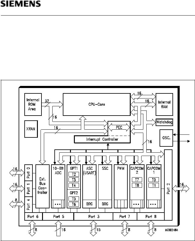
The architecture of the C167SR combines advantages of both RISC and CISC processors and of advanced peripheral subsystems in a very well-balanced way. The following block diagram gives an overview of the different on-chip components and of the advanced, high bandwidth internal bus structure of the C167SR.
Note: All time specifications refer to a CPU clock of 20 MHz (see definition in the AC Characteristics section).
Figure 3
Block Diagram
Semiconductor Group |
11 |

C167SR
Memory Organization
The memory space of the C167SR is configured in a Von Neumann architecture which means that code memory, data memory, registers and I/O ports are organized within the same linear address space which includes 16 MBytes. The entire memory space can be accessed bytewise or wordwise. Particular portions of the on-chip memory have additionally been made directly bitaddressable.
The C167SR is prepared to incorporate on-chip mask-programmable ROM or Flash Memory for code or constant data. Currently no ROM is integrated.
2 KBytes of on-chip Internal RAM are provided as a storage for user defined variables, for the system stack, general purpose register banks and even for code. A register bank can consist of up to 16 wordwide (R0 to R15) and/or bytewide (RL0, RH0, …, RL7, RH7) so-called General Purpose Registers (GPRs).
1024 bytes (2 × 512 bytes) of the address space are reserved for the Special Function Register areas (SFR space and ESFR space). SFRs are wordwide registers which are used for controlling and monitoring functions of the different on-chip units. Unused SFR addresses are reserved for future members of the C16x family.
2 KBytes of on-chip Extension RAM (XRAM) are provided to store user data, user stacks or code. The XRAM is accessed like external memory and therefore cannot be used for the system stack or for register banks and is not bitadressable. The XRAM allows 16-bit accesses with maximum speed.
In order to meet the needs of designs where more memory is required than is provided on chip, up to 16 MBytes of external RAM and/or ROM can be connected to the microcontroller.
External Bus Controller
All of the external memory accesses are performed by a particular on-chip External Bus Controller (EBC). It can be programmed either to Single Chip Mode when no external memory is required, or to one of four different external memory access modes, which are as follows:
–16-/18-/20-/24-bit Addresses, 16-bit Data, Demultiplexed
–16-/18-/20-/24-bit Addresses, 16-bit Data, Multiplexed
–16-/18-/20-/24-bit Addresses, 8-bit Data, Multiplexed
–16-/18-/20-/24-bit Addresses, 8-bit Data, Demultiplexed
In the demultiplexed bus modes, addresses are output on PORT1 and data is input/output on PORT0. In the multiplexed bus modes both addresses and data use PORT0 for input/output.
Important timing characteristics of the external bus interface (Memory Cycle Time, Memory TriState Time, Length of ALE and Read Write Delay) have been made programmable to allow the user the adaption of a wide range of different types of memories. In addition, different address ranges may be accessed with different bus characteristics. Up to 5 external CS signals can be generated in order to save external glue logic. Access to very slow memories is supported via a particular ‘Ready’ function. A HOLD/HLDA protocol is available for bus arbitration.
For applications which require less than 16 MBytes of external memory space, this address space can be restricted to 1 MByte, 256 KByte or to 64 KByte. In this case Port 4 outputs four, two or no address lines at all. It outputs all 8 address lines, if an address space of 16 MBytes is used.
Semiconductor Group |
12 |
C167SR
Central Processing Unit (CPU)
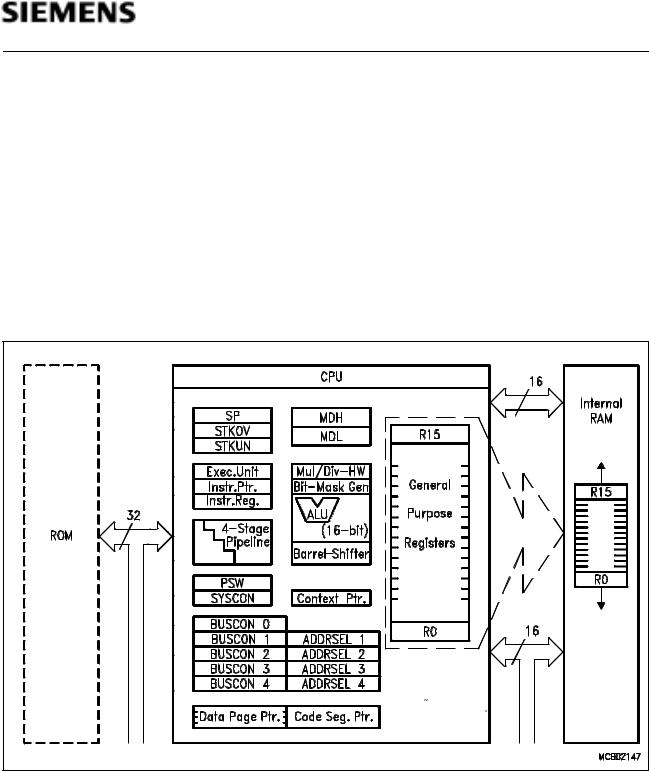
The main core of the CPU consists of a 4-stage instruction pipeline, a 16-bit arithmetic and logic unit (ALU) and dedicated SFRs. Additional hardware has been spent for a separate multiply and divide unit, a bit-mask generator and a barrel shifter.
Based on these hardware provisions, most of the C167SR’s instructions can be executed in just one machine cycle which requires 100 ns at 20-MHz CPU clock. For example, shift and rotate instructions are always processed during one machine cycle independent of the number of bits to be shifted. All multiple-cycle instructions have been optimized so that they can be executed very fast as well: branches in 2 cycles, a 16 × 16 bit multiplication in 5 cycles and a 32-/16 bit division in 10 cycles. Another pipeline optimization, the so-called ‘Jump Cache’, allows reducing the execution time of repeatedly performed jumps in a loop from 2 cycles to 1 cycle.
Figure 4
CPU Block Diagram
Semiconductor Group |
13 |

C167SR
The CPU disposes of an actual register context consisting of up to 16 wordwide GPRs which are physically allocated within the on-chip RAM area. A Context Pointer (CP) register determines the base address of the active register bank to be accessed by the CPU at a time. The number of register banks is only restricted by the available internal RAM space. For easy parameter passing, a register bank may overlap others.
A system stack of up to 2048 bytes is provided as a storage for temporary data. The system stack is allocated in the on-chip RAM area, and it is accessed by the CPU via the stack pointer (SP) register. Two separate SFRs, STKOV and STKUN, are implicitly compared against the stack pointer value upon each stack access for the detection of a stack overflow or underflow.
The high performance offered by the hardware implementation of the CPU can efficiently be utilized by a programmer via the highly efficient C167SR instruction set which includes the following instruction classes:
–Arithmetic Instructions
–Logical Instructions
–Boolean Bit Manipulation Instructions
–Compare and Loop Control Instructions
–Shift and Rotate Instructions
–Prioritize Instruction
–Data Movement Instructions
–System Stack Instructions
–Jump and Call Instructions
–Return Instructions
–System Control Instructions
–Miscellaneous Instructions
The basic instruction length is either 2 or 4 bytes. Possible operand types are bits, bytes and words. A variety of direct, indirect or immediate addressing modes are provided to specify the required operands.
Semiconductor Group |
14 |

C167SR
Interrupt System
With an interrupt response time within a range from just 250 ns to 600 ns (in case of internal program execution), the C167SR is capable of reacting very fast to the occurence of nondeterministic events.
The architecture of the C167SR supports several mechanisms for fast and flexible response to service requests that can be generated from various sources internal or external to the microcontroller. Any of these interrupt requests can be programmed to being serviced by the Interrupt Controller or by the Peripheral Event Controller (PEC).
In contrast to a standard interrupt service where the current program execution is suspended and a branch to the interrupt vector table is performed, just one cycle is ‘stolen’ from the current CPU activity to perform a PEC service. A PEC service implies a single byte or word data transfer between any two memory locations with an additional increment of either the PEC source or the destination pointer. An individual PEC transfer counter is implicity decremented for each PEC service except when performing in the continuous transfer mode. When this counter reaches zero, a standard interrupt is performed to the corresponding source related vector location. PEC services are very well suited, for example, for supporting the transmission or reception of blocks of data. The C167SR has 8 PEC channels each of which offers such fast interrupt-driven data transfer capabilities.
A separate control register which contains an interrupt request flag, an interrupt enable flag and an interrupt priority bitfield exists for each of the possible interrupt sources. Via its related register, each source can be programmed to one of sixteen interrupt priority levels. Once having been accepted by the CPU, an interrupt service can only be interrupted by a higher prioritized service request. For the standard interrupt processing, each of the possible interrupt sources has a dedicated vector location.
Fast external interrupt inputs are provided to service external interrupts with high precision requirements. These fast interrupt inputs feature programmable edge detection (rising edge, falling edge or both edges).
Software interrupts are supported by means of the ‘TRAP’ instruction in combination with an individual trap (interrupt) number.
The following table shows all of the possible C167SR interrupt sources and the corresponding hardware-related interrupt flags, vectors, vector locations and trap (interrupt) numbers:
Note: Three nodes in the table (X-Peripheral nodes) are prepared to accept interrupt requests from integrated X-Bus peripherals. Nodes, where no X-Peripherals are connected, may be used to generate software controlled interrupt requests by setting the respective XPnIR bit.
Semiconductor Group |
15 |

C167SR
Source of Interrupt or |
Request |
Enable |
Interrupt |
Vector |
Trap |
PEC Service Request |
Flag |
Flag |
Vector |
Location |
Number |
|
|
|
|
|
|
CAPCOM Register 0 |
CC0IR |
CC0IE |
CC0INT |
00’0040H |
10H |
CAPCOM Register 1 |
CC1IR |
CC1IE |
CC1INT |
00’0044H |
11H |
CAPCOM Register 2 |
CC2IR |
CC2IE |
CC2INT |
00’0048H |
12H |
CAPCOM Register 3 |
CC3IR |
CC3IE |
CC3INT |
00’004CH |
13H |
CAPCOM Register 4 |
CC4IR |
CC4IE |
CC4INT |
00’0050H |
14H |
CAPCOM Register 5 |
CC5IR |
CC5IE |
CC5INT |
00’0054H |
15H |
CAPCOM Register 6 |
CC6IR |
CC6IE |
CC6INT |
00’0058H |
16H |
CAPCOM Register 7 |
CC7IR |
CC7IE |
CC7INT |
00’005CH |
17H |
CAPCOM Register 8 |
CC8IR |
CC8IE |
CC8INT |
00’0060H |
18H |
CAPCOM Register 9 |
CC9IR |
CC9IE |
CC9INT |
00’0064H |
19H |
CAPCOM Register 10 |
CC10IR |
CC10IE |
CC10INT |
00’0068H |
1AH |
CAPCOM Register 11 |
CC11IR |
CC11IE |
CC11INT |
00’006CH |
1BH |
CAPCOM Register 12 |
CC12IR |
CC12IE |
CC12INT |
00’0070H |
1CH |
CAPCOM Register 13 |
CC13IR |
CC13IE |
CC13INT |
00’0074H |
1DH |
CAPCOM Register 14 |
CC14IR |
CC14IE |
CC14INT |
00’0078H |
1EH |
CAPCOM Register 15 |
CC15IR |
CC15IE |
CC15INT |
00’007CH |
1FH |
CAPCOM Register 16 |
CC16IR |
CC16IE |
CC16INT |
00’00C0H |
30H |
CAPCOM Register 17 |
CC17IR |
CC17IE |
CC17INT |
00’00C4H |
31H |
CAPCOM Register 18 |
CC18IR |
CC18IE |
CC18INT |
00’00C8H |
32H |
CAPCOM Register 19 |
CC19IR |
CC19IE |
CC19INT |
00’00CCH |
33H |
CAPCOM Register 20 |
CC20IR |
CC20IE |
CC20INT |
00’00D0H |
34H |
CAPCOM Register 21 |
CC21IR |
CC21IE |
CC21INT |
00’00D4H |
35H |
CAPCOM Register 22 |
CC22IR |
CC22IE |
CC22INT |
00’00D8H |
36H |
CAPCOM Register 23 |
CC23IR |
CC23IE |
CC23INT |
00’00DCH |
37H |
CAPCOM Register 24 |
CC24IR |
CC24IE |
CC24INT |
00’00E0H |
38H |
CAPCOM Register 25 |
CC25IR |
CC25IE |
CC25INT |
00’00E4H |
39H |
CAPCOM Register 26 |
CC26IR |
CC26IE |
CC26INT |
00’00E8H |
3AH |
CAPCOM Register 27 |
CC27IR |
CC27IE |
CC27INT |
00’00ECH |
3BH |
CAPCOM Register 28 |
CC28IR |
CC28IE |
CC28INT |
00’00E0H |
3CH |
CAPCOM Register 29 |
CC29IR |
CC29IE |
CC29INT |
00’0110H |
44H |
CAPCOM Register 30 |
CC30IR |
CC30IE |
CC30INT |
00’0114H |
45H |
CAPCOM Register 31 |
CC31IR |
CC31IE |
CC31INT |
00’0118H |
46H |
CAPCOM Timer 0 |
T0IR |
T0IE |
T0INT |
00’0080H |
20H |
Semiconductor Group |
|
16 |
|
|
|

C167SR
Source of Interrupt or |
Request |
Enable |
Interrupt |
Vector |
Trap |
PEC Service Request |
Flag |
Flag |
Vector |
Location |
Number |
|
|
|
|
|
|
CAPCOM Timer 1 |
T1IR |
T1IE |
T1INT |
00’0084H |
21H |
CAPCOM Timer 7 |
T7IR |
T7IE |
T7INT |
00’00F4H |
3DH |
CAPCOM Timer 8 |
T8IR |
T8IE |
T8INT |
00’00F8H |
3EH |
GPT1 Timer 2 |
T2IR |
T2IE |
T2INT |
00’0088H |
22H |
GPT1 Timer 3 |
T3IR |
T3IE |
T3INT |
00’008CH |
23H |
GPT1 Timer 4 |
T4IR |
T4IE |
T4INT |
00’0090H |
24H |
GPT2 Timer 5 |
T5IR |
T5IE |
T5INT |
00’0094H |
25H |
GPT2 Timer 6 |
T6IR |
T6IE |
T6INT |
00’0098H |
26H |
GPT2 CAPREL Register |
CRIR |
CRIE |
CRINT |
00’009CH |
27H |
A/D Conversion Complete |
ADCIR |
ADCIE |
ADCINT |
00’00A0H |
28H |
A/D Overrun Error |
ADEIR |
ADEIE |
ADEINT |
00’00A4H |
29H |
ASC0 Transmit |
S0TIR |
S0TIE |
S0TINT |
00’00A8H |
2AH |
ASC0 Transmit Buffer |
S0TBIR |
S0TBIE |
S0TBINT |
00’011CH |
47H |
ASC0 Receive |
S0RIR |
S0RIE |
S0RINT |
00’00ACH |
2BH |
ASC0 Error |
S0EIR |
S0EIE |
S0EINT |
00’00B0H |
2CH |
SSC Transmit |
SCTIR |
SCTIE |
SCTINT |
00’00B4H |
2DH |
SSC Receive |
SCRIR |
SCRIE |
SCRINT |
00’00B8H |
2EH |
SSC Error |
SCEIR |
SCEIE |
SCEINT |
00’00BCH |
2FH |
PWM Channel 0...3 |
PWMIR |
PWMIE |
PWMINT |
00’00FCH |
3FH |
X-Peripheral Node |
XP0IR |
XP0IE |
XP0INT |
00’0100H |
40H |
X-Peripheral Node |
XP1IR |
XP1IE |
XP1INT |
00’0104H |
41H |
X-Peripheral Node |
XP2IR |
XP2IE |
XP2INT |
00’0108H |
42H |
PLL Unlock |
XP3IR |
XP3IE |
XP3INT |
00’010CH |
43H |
Semiconductor Group |
17 |
 Loading...