


Microcomputer Components
16-Bit CMOS Single-Chip Microcontroller
C165
Data Sheet 09.94

C16x-Family of |
C165 |
High-Performance CMOS 16-Bit Microcontrollers
Preliminary
C165 16-Bit Microcontroller
●High Performance 16-bit CPU with 4-Stage Pipeline
●100 ns Instruction Cycle Time at 20-MHz CPU Clock
●500 ns Multiplication (16 × 16 bits), 1 µs Division (32 / 16 bit)
●Enhanced Boolean Bit Manipulation Facilities
●Additional Instructions to Support HLL and Operating Systems
●Register-Based Design with Multiple Variable Register Banks
●Single-Cycle Context Switching Support
●Up to 16 MBytes Linear Address Space for Code and Data
●2 KBytes On-Chip RAM
●4 KBytes On-Chip ROM (RM types only)
●Programmable External Bus Characteristics for Different Address Ranges
●8-Bit or 16-Bit External Data Bus
●Multiplexed or Demultiplexed External Address/Data Buses
●Five Programmable Chip-Select Signals
●Holdand Hold-Acknowledge Bus Arbitration Support
●1024 Bytes On-Chip Special Function Register Area
●Idle and Power Down Modes
●8-Channel Interrupt-Driven Single-Cycle Data Transfer Facilities via Peripheral Event Controller (PEC)
●16-Priority-Level Interrupt System with 28 Sources, Sample-Rate down to 50 ns
●Two Multi-Functional General Purpose Timer Units with 5 Timers
●Two Serial Channels (Synchronous/Asynchronous and High-Speed-Synchronous)
●Programmable Watchdog Timer
●Up to 77 General Purpose I/O Lines
●Supported by a Wealth of Development Tools like C-Compilers, Macro-Assembler Packages, Emulators, Evaluation Boards, HLL-Debuggers, Simulators, Logic Analyzer Disassemblers, Programming Boards
●On-Chip Bootstrap Loader
●100-Pin MQFP Package (EIAJ)
●100-Pin TQFP Package (Thin QFP)
09.94 Data Sheet Addendum – Attention
The C165 is offered in two different packages:
P-MQFP-100: |
rectangular package |
P-TQFP-100: |
square package. |
For the pin configurations please refer to page 3 (P-MQFP-100) and page 8 (P-TQFP-100) of the 09.94 C165 Data Sheet. Please note that the table “Pin Definition and Functions” on pages 9 through 12 lists the pin numbers for the MQFP package only.
The pin numbers for the TQFP package are different and should be taken from the pin configuration on page 3.
Semiconductor Group |
1 |
09.94 |
C165
Introduction
The C165 is a new derivative of the Siemens SAB 80C166 family of full featured single-chip CMOS microcontrollers. It combines high CPU performance (up to 10 million instructions per second) with high peripheral functionality and enhanced IO-capabilities.
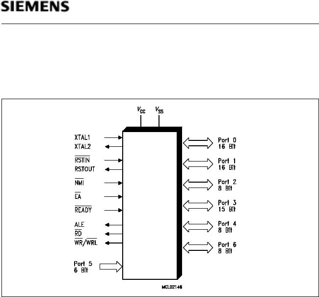
C165
Figure 1
Logic Symbol
Ordering Information
Type |
Ordering Code |
Package |
Function |
|
|
|
|
SAB-C165-RM |
Q67121-D... |
P-MQFP-100-2 |
16-bit microcontroller with |
|
|
|
2 KByte RAM and 4 KByte ROM |
|
|
|
Temperature range 0 to +70 ˚C |
|
|
|
|
SAB-C165-LM |
Q67121-C862 |
P-MQFP-100-2 |
16-bit microcontroller with |
|
|
|
2 KByte RAM |
|
|
|
Temperature range 0 to +70 ˚C |
|
|
|
|
SAF-C165-LM |
Q67121-C923 |
P-MQFP-100-2 |
16-bit microcontroller with |
|
|
|
2 KByte RAM |
|
|
|
Temperature range -40 to +85 ˚C |
|
|
|
|
Note: The ordering codes (Q67121-D...) for the Mask-ROM versions are defined for each product after verification of the respective ROM code.
Semiconductor Group |
2 |
C165
Ordering Information
Type |
Ordering Code |
Package |
Function |
|
|
|
|
SAB-C165-RF |
Q67121-D... |
P-TQFP-100-3 |
16-bit microcontroller with |
|
|
|
2 KByte RAM and 4 KByte ROM |
|
|
|
Temperature range 0 to +70 ˚C |
|
|
|
|
SAB-C165-LF |
Q67121-C941 |
P-TQFP-100-3 |
16-bit microcontroller with |
|
|
|
2 KByte RAM |
|
|
|
Temperature range 0 to +70 ˚C |
|
|
|
|
Note: The ordering codes (Q67121-D...) for the Mask-ROM versions are defined for each product after verification of the respective ROM code.
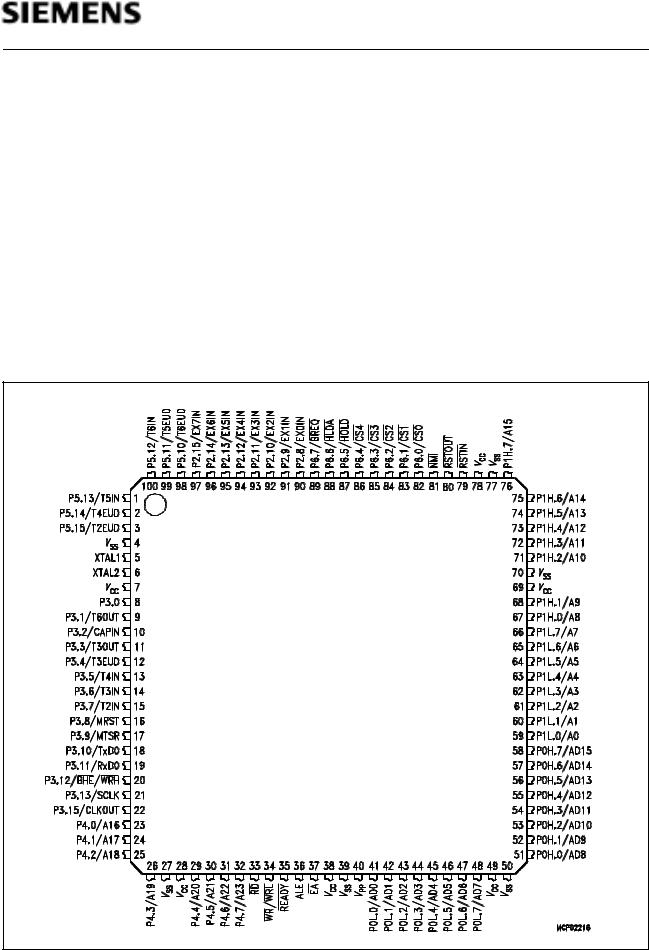
Pin Configuration TQFP Package
(top view)
C165 |
Figure 2
Semiconductor Group |
3 |

C165
Pin Configuration MQFP Package
(top view)
C165
Figure 3
Semiconductor Group |
4 |

C165
Pin Definitions and Functions
Symbol |
Pin |
Input (I) |
Function |
|
|
|
|
|
No. |
Output (O) |
|
|
|
|
|
|
|
|
|
||||
P5.10 – |
100 |
I |
Port 5 is a 6-bit input-only port with Schmitt-Trigger |
||||
P5.15 |
1 - 5 |
I |
characteristics. The pins of Port 5 also serve as timer inputs: |
||||
|
100 |
I |
P5.10 |
T6EUD |
GPT2 Timer T6 Ext.Up/Down Ctrl.Input |
||
|
1 |
I |
P5.11 |
T5EUD |
GPT2 Timer T5 Ext.Up/Down Ctrl.Input |
||
|
2 |
I |
P5.12 |
T6IN |
GPT2 Timer T6 Count Input |
||
|
3 |
I |
P5.13 |
T5IN |
GPT2 Timer T5 Count Input |
||
|
4 |
I |
P5.14 |
T4EUD |
GPT1 Timer T4 Ext.Up/Down Ctrl.Input |
||
|
5 |
I |
P5.15 |
T2EUD |
GPT1 Timer T2 Ext.Up/Down Ctrl.Input |
||
|
|
|
|
|
|||
XTAL1 |
7 |
I |
XTAL1: |
Input to the oscillator amplifier and input to the |
|||
|
|
|
|
internal clock generator |
|||
XTAL2 |
8 |
O |
XTAL2: |
Output of the oscillator amplifier circuit. |
|||
|
|
|
To clock the device from an external source, drive XTAL1, |
||||
|
|
|
while leaving XTAL2 unconnected. Minimum and maximum |
||||
|
|
|
high/low and rise/fall times specified in the AC Characteristics |
||||
|
|
|
must be observed. |
|
|||
|
|
|
|
||||
P3.0 – |
10 – |
I/O |
Port 3 is a 15-bit (P3.14 is missing) bidirectional I/O port. It is |
||||
P3.13, |
23, |
I/O |
bit-wise programmable for input or output via direction bits. |
||||
P3.15 |
24 |
I/O |
For a pin configured as input, the output driver is put into high- |
||||
|
|
|
impedance state. Port 3 outputs can be configured as push/ |
||||
|
|
|
pull or open drain drivers. |
||||
|
|
|
The following Port 3 pins also serve for alternate functions: |
||||
|
11 |
O |
P3.1 |
T6OUT |
GPT2 Timer T6 Toggle Latch Output |
||
|
12 |
I |
P3.2 |
CAPIN |
GPT2 Register CAPREL Capture Input |
||
|
13 |
O |
P3.3 |
T3OUT |
GPT1 Timer T3 Toggle Latch Output |
||
|
14 |
I |
P3.4 |
T3EUD |
GPT1 Timer T3 Ext.Up/Down Ctrl.Input |
||
|
15 |
I |
P3.5 |
T4IN |
GPT1 Timer T4 Input for |
||
|
|
|
|
|
|
|
Count/Gate/Reload/Capture |
|
16 |
I |
P3.6 |
T3IN |
GPT1 Timer T3 Count/Gate Input |
||
|
17 |
I |
P3.7 |
T2IN |
GPT1 Timer T2 Input for |
||
|
|
|
|
|
|
|
Count/Gate/Reload/Capture |
|
18 |
I/O |
P3.8 |
MRST |
SSC Master-Rec./Slave-Transmit I/O |
||
|
19 |
I/O |
P3.9 |
MTSR |
SSC Master-Transmit/Slave-Rec. O/I |
||
|
20 |
O |
P3.10 |
T×D0 |
ASC0 Clock/Data Output (Asyn./Syn.) |
||
|
21 |
I/O |
P3.11 |
R×D0 |
ASC0 Data Input (Asyn.) or I/O (Syn.) |
||
|
22 |
O |
P3.12 |
|
|
|
Ext. Memory High Byte Enable Signal, |
|
BHE |
||||||
|
|
O |
|
|
|
Ext. Memory High Byte Write Strobe |
|
|
|
|
WRH |
||||
|
23 |
I/O |
P3.13 |
SCLK |
SSC Master Clock Outp./Slave Cl. Inp. |
||
|
24 |
O |
P3.15 |
CLKOUT |
System Clock Output (=CPU Clock) |
||
|
|
|
|
|
|
|
|
Semiconductor Group |
5 |

C165
Pin Definitions and Functions (cont’d)
Symbol |
Pin |
Input (I) |
Function |
|
|
|
|
|
|
|
|
|||||
|
|
|
|
|
|
No. |
Output (O) |
|
|
|
|
|
|
|
|
|
|
|
|
|
|||||||||||||
P4.0 – |
25 - 28, |
I/O |
Port 4 is an 8-bit bidirectional I/O port. It is bit-wise |
|||||||||||||
P4.7 |
31 - 34 |
|
programmable for input or output via direction bits. For a pin |
|||||||||||||
|
|
|
|
|
|
|
|
configured as input, the output driver is put into high- |
||||||||
|
|
|
|
|
|
|
|
impedance state. |
|
|
|
|
|
|
|
|
|
|
|
|
|
|
|
|
In case of an external bus configuration, Port 4 can be used to |
||||||||
|
|
|
|
|
|
|
|
output the segment address lines: |
||||||||
|
|
|
|
|
|
25 |
O |
P4.0 |
A16 |
Least Significant Segment Addr. Line |
||||||
|
|
|
|
|
|
... |
... |
... |
... |
... |
|
|
|
|
|
|
|
|
|
|
|
|
34 |
O |
P4.7 |
A23 |
Most Significant Segment Addr. Line |
||||||
|
|
|
|
|
|
|
|
|
|
|
|
|||||
|
|
|
|
|
|
35 |
O |
External Memory Read Strobe. |
|
|
is activated for every |
|||||
RD |
RD |
|||||||||||||||
|
|
|
|
|
|
|
|
external instruction or data read access. |
||||||||
|
|
|
|
|
|
|
|
|
|
|||||||
|
|
|
|
|
|
36 |
O |
External Memory Write Strobe. In |
|
-mode this pin is |
||||||
WR/ |
WR |
|||||||||||||||
|
|
|
|
|
|
activated for every external data write access. In |
|
-mode |
||||||||
WRL |
|
|
WRL |
|||||||||||||
|
|
|
|
|
|
|
|
this pin is activated for low byte data write accesses on a 16- |
||||||||
|
|
|
|
|
|
|
|
bit bus, and for every data write access on an 8-bit bus. See |
||||||||
|
|
|
|
|
|
|
|
WRCFG in register SYSCON for mode selection. |
||||||||
|
|
|
|
|
|
|||||||||||
|
|
|
|
|
|
37 |
I |
Ready Input. When the Ready function is enabled, a high |
||||||||
READY |
||||||||||||||||
|
|
|
|
|
|
|
|
level at this pin during an external memory access will force |
||||||||
|
|
|
|
|
|
|
|
the insertion of memory cycle time waitstates until the pin |
||||||||
|
|
|
|
|
|
|
|
returns to a low level. |
|
|
|
|
|
|
|
|
|
|
|
|
|||||||||||||
ALE |
38 |
O |
Address Latch Enable Output. Can be used for latching the |
|||||||||||||
|
|
|
|
|
|
|
|
address into external memory or an address latch in the |
||||||||
|
|
|
|
|
|
|
|
multiplexed bus modes. |
||||||||
|
|
|
|
|
||||||||||||
|
|
39 |
I |
External Access Enable pin. A low level at this pin during and |
||||||||||||
EA |
||||||||||||||||
|
|
|
|
|
|
|
|
after Reset forces the C165 to begin instruction execution out |
||||||||
|
|
|
|
|
|
|
|
of external memory. A high level forces execution out of the |
||||||||
|
|
|
|
|
|
|
|
internal ROM. The C165 must have this pin tied to ‘0’. |
||||||||
|
|
|
|
|
|
|
|
|
|
|
|
|
|
|
|
|
Semiconductor Group |
6 |

C165
Pin Definitions and Functions (cont’d)
Symbol |
Pin |
Input (I) |
Function |
|
|
|
|
|
|
||||||
|
|
|
|
No. |
Output (O) |
|
|
|
|
|
|
|
|
|
|
|
|
|
|
||||||||||||
PORT0: |
|
I/O |
PORT0 consists of the two 8-bit bidirectional I/O ports P0L |
||||||||||||
P0L.0 – |
43 – |
|
and P0H. It is bit-wise programmable for input or output via |
||||||||||||
P0L.7, |
50 |
|
direction bits. For a pin configured as input, the output driver |
||||||||||||
P0H.0 - |
53 – |
|
is put into high-impedance state. |
|
|
|
|||||||||
P0H.7 |
60 |
|
In case of an external bus configuration, PORT0 serves as |
||||||||||||
|
|
|
|
|
|
the address (A) and address/data (AD) bus in multiplexed bus |
|||||||||
|
|
|
|
|
|
modes and as the data (D) bus in demultiplexed bus modes. |
|||||||||
|
|
|
|
|
|
Demultiplexed bus modes: |
|
|
|
||||||
|
|
|
|
|
|
Data Path Width: |
8-bit |
16-bit |
|||||||
|
|
|
|
|
|
P0L.0 – P0L.7: |
D0 – D7 |
D0 - D7 |
|||||||
|
|
|
|
|
|
P0H.0 – P0H.7: |
I/O |
D8 - D15 |
|||||||
|
|
|
|
|
|
Multiplexed bus modes: |
|
|
|
||||||
|
|
|
|
|
|
Data Path Width: |
8-bit |
16-bit |
|||||||
|
|
|
|
|
|
P0L.0 – P0L.7: |
AD0 – AD7 |
AD0 - AD7 |
|||||||
|
|
|
|
|
|
P0H.0 – P0H.7: |
A8 - A15 |
AD8 - AD15 |
|||||||
|
|
|
|
||||||||||||
PORT1: |
|
I/O |
PORT1 consists of the two 8-bit bidirectional I/O ports P1L |
||||||||||||
P1L.0 – |
61 - |
|
and P1H. It is bit-wise programmable for input or output via |
||||||||||||
P1L.7, |
68 |
|
direction bits. For a pin configured as input, the output driver |
||||||||||||
P1H.0 - |
69 - 70, |
|
is put into high-impedance state. PORT1 is used as the 16-bit |
||||||||||||
P1H.7 |
73 - 78 |
|
address bus (A) in demultiplexed bus modes and also after |
||||||||||||
|
|
|
|
|
|
switching from a demultiplexed bus mode to a multiplexed |
|||||||||
|
|
|
|
|
|
bus mode. |
|
|
|
|
|
|
|||
|
|
|
|
|
|
|
|||||||||
|
|
|
|
81 |
I |
Reset Input with Schmitt-Trigger characteristics. A low level at |
|||||||||
RSTIN |
|||||||||||||||
|
|
|
|
|
|
this pin for a specified duration while the oscillator is running |
|||||||||
|
|
|
|
|
|
resets the C165. An internal pullup resistor permits power-on |
|||||||||
|
|
|
|
|
|
reset using only a capacitor connected to VSS. |
|||||||||
|
|
|
|
|
|
||||||||||
|
|
|
|
82 |
O |
Internal Reset Indication Output. This pin is set to a low level |
|||||||||
RSTOUT |
|||||||||||||||
|
|
|
|
|
|
when the part is executing either a hardware-, a softwareor a |
|||||||||
|
|
|
|
|
|
watchdog timer reset. |
|
remains low until the EINIT |
|||||||
|
|
|
|
|
|
RSTOUT |
|||||||||
|
|
|
|
|
|
(end of initialization) instruction is executed. |
|||||||||
|
|
|
|
|
|||||||||||
|
|
83 |
I |
Non-Maskable Interrupt Input. A high to low transition at this |
|||||||||||
NMI |
|||||||||||||||
|
|
|
|
|
|
pin causes the CPU to vector to the NMI trap routine. When |
|||||||||
|
|
|
|
|
|
the PWRDN (power down) instruction is executed, the |
|
|
|||||||
|
|
|
|
|
|
NMI |
|||||||||
|
|
|
|
|
|
pin must be low in order to force the C165 to go into power |
|||||||||
|
|
|
|
|
|
down mode. If |
|
|
is high, when PWRDN is executed, the |
||||||
|
|
|
|
|
|
NMI |
|||||||||
|
|
|
|
|
|
part will continue to run in normal mode. |
|
|
|
||||||
|
|
|
|
|
|
If not used, pin |
|
should be pulled high externally. |
|||||||
|
|
|
|
|
|
NMI |
|||||||||
|
|
|
|
|
|
|
|
|
|
|
|
|
|
|
|
Semiconductor Group |
7 |

C165
Pin Definitions and Functions (cont’d)
Symbol |
Pin |
Input (I) |
Function |
|
|
|
|
|
|
|
|
No. |
Output (O) |
|
|
|
|
|
|
|
|
|
|
|
|
|||||||
P6.0 – |
84 - |
I/O |
Port 6 is an 8-bit bidirectional I/O port. It is bit-wise |
|||||||
P6.7 |
91 |
|
programmable for input or output via direction bits. For a pin |
|||||||
|
|
|
configured as input, the output driver is put into high- |
|||||||
|
|
|
impedance state. Port 6 outputs can be configured as push/ |
|||||||
|
|
|
pull or open drain drivers. |
|||||||
|
|
|
The following Port 6 pins also serve for alternate functions: |
|||||||
|
84 |
O |
P6.0 |
|
|
|
|
|
|
Chip Select 0 Output |
|
CS0 |
|||||||||
|
... |
... |
... |
... |
|
|
|
|
|
... |
|
88 |
O |
P6.4 |
|
|
|
|
|
Chip Select 4 Output |
|
|
CS4 |
|||||||||
|
89 |
I |
P6.5 |
|
|
|
|
External Master Hold Request Input |
||
|
HOLD |
|||||||||
|
90 |
O |
P6.6 |
|
|
|
Hold Acknowledge Output |
|||
|
HLDA |
|||||||||
|
91 |
O |
P6.7 |
|
|
Bus Request Output |
||||
|
BREQ |
|||||||||
|
|
|
|
|||||||
P2.8 – |
92 - |
I/O |
Port 2 is an 8-bit bidirectional I/O port. It is bit-wise |
|||||||
P2.15 |
99 |
|
programmable for input or output via direction bits. For a pin |
|||||||
|
|
|
configured as input, the output driver is put into high- |
|||||||
|
|
|
impedance state. Port 2 outputs can be configured as push/ |
|||||||
|
|
|
pull or open drain drivers. |
|||||||
|
|
|
The following Port 2 pins also serve for alternate functions: |
|||||||
|
92 |
I |
P2.8 |
EX0IN |
Fast External Interrupt 0 Input |
|||||
|
... |
... |
... |
... |
|
|
|
|
|
... |
|
99 |
I |
P2.15 |
EX7IN |
Fast External Interrupt 7 Input |
|||||
|
|
|
|
|||||||
VPP |
42 |
- |
Flash programming voltage. This pin accepts the |
|||||||
|
|
|
programming voltage for flash versions of the C165. |
|||||||
|
|
|
Note: This pin is not connected (NC) on non-flash versions. |
|||||||
|
|
|
|
|||||||
VCC |
9, 30, |
- |
Digital Supply Voltage: |
|||||||
|
40, 51, |
|
+ 5 V during normal operation and idle mode. |
|||||||
|
71, 80 |
|
≥ 2.5 V during power down mode |
|||||||
|
|
|
|
|
||||||
VSS |
6, 29, |
- |
Digital Ground. |
|
||||||
|
41, 52, |
|
|
|
|
|
|
|
|
|
|
72, 79 |
|
|
|
|
|
|
|
|
|
|
|
|
|
|
|
|
|
|
|
|
Semiconductor Group |
8 |
C165
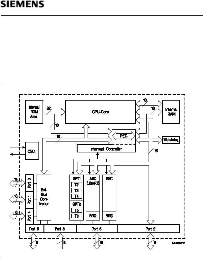
Functional Description
The architecture of the C165 combines advantages of both RISC and CISC processors and of advanced peripheral subsystems in a very well-balanced way. The following block diagram gives an overview of the different on-chip components and of the advanced, high bandwidth internal bus structure of the C165.
Note: All time specifications refer to a CPU clock of 20 MHz (see definition in the AC Characteristics section).
Figure 4
Block Diagram
Semiconductor Group |
9 |
C165
Memory Organization
The memory space of the C165 is configured in a Von Neumann architecture which means that code memory, data memory, registers and I/O ports are organized within the same linear address space which includes 16 MBytes. The entire memory space can be accessed bytewise or wordwise. Particular portions of the on-chip memory have additionally been made directly bit addressable.
The C165 is prepared to incorporate on-chip mask-programmable ROM for code or constant data. Currently no ROM is integrated.
2 KBytes of on-chip RAM are provided as a storage for user defined variables, for the system stack, general purpose register banks and even for code. A register bank can consist of up to 16 wordwide (R0 to R15) and/or bytewide (RL0, RH0, …, RL7, RH7) so-called General Purpose Registers (GPRs).
1024 bytes (2 * 512 bytes) of the address space are reserved for the Special Function Register areas (SFR space and ESFR space). SFRs are wordwide registers which are used for controlling and monitoring functions of the different on-chip units. Unused SFR addresses are reserved for future members of the C165 family.
In order to meet the needs of designs where more memory is required than is provided on chip, up to 16 MBytes of external RAM and/or ROM can be connected to the microcontroller.
External Bus Controller
All of the external memory accesses are performed by a particular on-chip External Bus Controller (EBC). It can be programmed either to Single Chip Mode when no external memory is required, or to one of four different external memory access modes, which are as follows:
–16-/18-/20-/24-bit Addresses, 16-bit Data, Demultiplexed
–16-/18-/20-/24-bit Addresses, 16-bit Data, Multiplexed
–16-/18-/20-/24-bit Addresses, 8-bit Data, Multiplexed
–16-/18-/20-/24-bit Addresses, 8-bit Data, Demultiplexed
In the demultiplexed bus modes, addresses are output on PORT1 and data is input/output on PORT0. In the multiplexed bus modes both addresses and data use PORT0 for input/output.
Important timing characteristics of the external bus interface (Memory Cycle Time, Memory TriState Time, Length of ALE and Read Write Delay) have been made programmable to allow the user the adaption of a wide range of different types of memories. In addition, different address ranges may be accessed with different bus characteristics. Up to 5 external CS signals can be generated in order to save external glue logic. Access to very slow memories is supported via a particular ‘Ready’ function. A HOLD/HLDA protocol is available for bus arbitration.
For applications which require less than 16 MBytes of external memory space, this address space can be restricted to 1 MByte, 256 KByte or to 64 KByte. In this case Port 4 outputs four, two or no address lines at all. It outputs all 8 address lines, if an address space of 16 MBytes is used.
Semiconductor Group |
10 |
C165
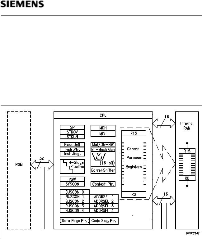
Central Processing Unit (CPU)
The main core of the CPU consists of a 4-stage instruction pipeline, a 16-bit arithmetic and logic unit (ALU) and dedicated SFRs. Additional hardware has been spent for a separate multiply and divide unit, a bit-mask generator and a barrel shifter.
Based on these hardware provisions, most of the C165’s instructions can be executed in just one machine cycle which requires 100 ns at 20-MHz CPU clock. For example, shift and rotate instructions are always processed during one machine cycle independent of the number of bits to be shifted. All multiple-cycle instructions have been optimized so that they can be executed very fast as well: branches in 2 cycles, a 16 × 16 bit multiplication in 5 cycles and a 32-/16 bit division in 10 cycles. Another pipeline optimization, the so-called ‘Jump Cache’, allows reducing the execution time of repeatedly performed jumps in a loop from 2 cycles to 1 cycle.
Figure 5
CPU Block Diagram
Semiconductor Group |
11 |

C165
The CPU disposes of an actual register context consisting of up to 16 wordwide GPRs which are physically allocated within the on-chip RAM area. A Context Pointer (CP) register determines the base address of the active register bank to be accessed by the CPU at a time. The number of register banks is only restricted by the available internal RAM space. For easy parameter passing, a register bank may overlap others.
A system stack of up to 2048 bytes is provided as a storage for temporary data. The system stack is allocated in the on-chip RAM area, and it is accessed by the CPU via the stack pointer (SP) register. Two separate SFRs, STKOV and STKUN, are implicitly compared against the stack pointer value upon each stack access for the detection of a stack overflow or underflow.
The high performance offered by the hardware implementation of the CPU can efficiently be utilized by a programmer via the highly efficient C165 instruction set which includes the following instruction classes:
–Arithmetic Instructions
–Logical Instructions
–Boolean Bit Manipulation Instructions
–Compare and Loop Control Instructions
–Shift and Rotate Instructions
–Prioritize Instruction
–Data Movement Instructions
–System Stack Instructions
–Jump and Call Instructions
–Return Instructions
–System Control Instructions
–Miscellaneous Instructions
The basic instruction length is either 2 or 4 bytes. Possible operand types are bits, bytes and words. A variety of direct, indirect or immediate addressing modes are provided to specify the required operands.
Semiconductor Group |
12 |

C165
Interrupt System
With an interrupt response time within a range from just 250 ns to 600 ns (in case of internal program execution), the C165 is capable of reacting very fast to the occurrence of non-deterministic events.
The architecture of the C165 supports several mechanisms for fast and flexible response to service requests that can be generated from various sources internal or external to the microcontroller. Any of these interrupt requests can be programmed to being serviced by the Interrupt Controller or by the Peripheral Event Controller (PEC).
In contrast to a standard interrupt service where the current program execution is suspended and a branch to the interrupt vector table is performed, just one cycle is ‘stolen’ from the current CPU activity to perform a PEC service. A PEC service implies a single byte or word data transfer between any two memory locations with an additional increment of either the PEC source or the destination pointer. An individual PEC transfer counter is implicity decremented for each PEC service except when performing in the continuous transfer mode. When this counter reaches zero, a standard interrupt is performed to the corresponding source related vector location. PEC services are very well suited, for example, for supporting the transmission or reception of blocks of data. The C165 has 8 PEC channels each of which offers such fast interrupt-driven data transfer capabilities.
A separate control register which contains an interrupt request flag, an interrupt enable flag and an interrupt priority bitfield exists for each of the possible interrupt sources. Via its related register, each source can be programmed to one of sixteen interrupt priority levels. Once having been accepted by the CPU, an interrupt service can only be interrupted by a higher prioritized service request. For the standard interrupt processing, each of the possible interrupt sources has a dedicated vector location.
Fast external interrupt inputs are provided to service external interrupts with high precision requirements. These fast interrupt inputs feature programmable edge detection (rising edge, falling edge or both edges).
Software interrupts are supported by means of the ‘TRAP’ instruction in combination with an individual trap (interrupt) number.
The following table shows all of the possible C165 interrupt sources and the corresponding hardware-related interrupt flags, vectors, vector locations and trap (interrupt) numbers:
Note: Four nodes in the table (X-Peripheral nodes) are prepared to accept interrupt requests from integrated X-Bus peripherals. Nodes, where no X-Peripherals are connected, may be used to generate software controlled interrupt requests by setting the respective XPnIR bit. Also the three listed Software Nodes can be used for this purpose.
Semiconductor Group |
13 |

C165
Source of Interrupt or |
Request |
Enable |
Interrupt |
Vector |
Trap |
PEC Service Request |
Flag |
Flag |
Vector |
Location |
Number |
|
|
|
|
|
|
External Interrupt 0 |
CC8IR |
CC8IE |
CC8INT |
00’0060H |
18H |
External Interrupt 1 |
CC9IR |
CC9IE |
CC9INT |
00’0064H |
19H |
External Interrupt 2 |
CC10IR |
CC10IE |
CC10INT |
00’0068H |
1AH |
External Interrupt 3 |
CC11IR |
CC11IE |
CC11INT |
00’006CH |
1BH |
External Interrupt 4 |
CC12IR |
CC12IE |
CC12INT |
00’0070H |
1CH |
External Interrupt 5 |
CC13IR |
CC13IE |
CC13INT |
00’0074H |
1DH |
External Interrupt 6 |
CC14IR |
CC14IE |
CC14INT |
00’0078H |
1EH |
External Interrupt 7 |
CC15IR |
CC15IE |
CC15INT |
00’007CH |
1FH |
GPT1 Timer 2 |
T2IR |
T2IE |
T2INT |
00’0088H |
22H |
GPT1 Timer 3 |
T3IR |
T3IE |
T3INT |
00’008CH |
23H |
GPT1 Timer 4 |
T4IR |
T4IE |
T4INT |
00’0090H |
24H |
GPT2 Timer 5 |
T5IR |
T5IE |
T5INT |
00’0094H |
25H |
GPT2 Timer 6 |
T6IR |
T6IE |
T6INT |
00’0098H |
26H |
GPT2 CAPREL Register |
CRIR |
CRIE |
CRINT |
00’009CH |
27H |
ASC0 Transmit |
S0TIR |
S0TIE |
S0TINT |
00’00A8H |
2AH |
ASC0 Transmit Buffer |
S0TBIR |
S0TBIE |
S0TBINT |
00’011CH |
47H |
ASC0 Receive |
S0RIR |
S0RIE |
S0RINT |
00’00ACH |
2BH |
ASC0 Error |
S0EIR |
S0EIE |
S0EINT |
00’00B0H |
2CH |
SSC Transmit |
SCTIR |
SCTIE |
SCTINT |
00’00B4H |
2DH |
SSC Receive |
SCRIR |
SCRIE |
SCRINT |
00’00B8H |
2EH |
SSC Error |
SCEIR |
SCEIE |
SCEINT |
00’00BCH |
2FH |
X-Peripheral Node 0 |
XP0IR |
XP0IE |
XP0INT |
00’0100H |
40H |
X-Peripheral Node 1 |
XP1IR |
XP1IE |
XP1INT |
00’0104H |
41H |
X-Peripheral Node 2 |
XP2IR |
XP2IE |
XP2INT |
00’0108H |
42H |
X-Peripheral Node 3 |
XP3IR |
XP3IE |
XP3INT |
00’010CH |
43H |
Software Node |
CC29IR |
CC29IE |
CC29INT |
00’0110H |
44H |
Software Node |
CC30IR |
CC30IE |
CC30INT |
00’0114H |
45H |
Software Node |
CC31IR |
CC31IE |
CC31INT |
00’0118H |
46H |
Semiconductor Group |
14 |
 Loading...