


RED PLCD5580 YELLOW PLCD5581
HIGH EFFICIENCY RED PLCD5582
GREEN PLCD5583
HIGH EFFICIENCY GREEN PLCD5584 Low Power 0.145” 8-Character, 5x5 Dot Matrix Parallel Input Alphanumeric Intelligent Display
FEATURES
•Eight 0.145” (3.68 mm) High 5 x 5 Dot Matrix Characters in Red, Yellow, High Efficiency Red, Green, or High Efficiency Green
•Built-in 2 Page, 256 Character ROM. Both Pages Mask Programmable for Custom Fonts
•Built-in Decoders, Multiplexers and Drivers
•Wide Viewing Angle, X Axis ±50°, Y Axis ±65°
•Programmable Features:
–Individual Flashing Character
–Full Display Blinking
–Multi-Level Dimming and Blanking
–Clear Function
–Lamp Test
•Internal or External Clock
•End Stackable Dual-In-Line Plastic Package
•Low Power: 20% Less Power Consumption Than 5 X 7 Format
Package Dimensions in inches (mm)
|
1.680 (42.67) max. |
|
0.105 |
|
0.086 |
||
|
0.210 |
|
|
|
|||
|
|
|
|
(2.19) |
|||
|
(5.34) |
|
|
(2.67) |
|
||
0.145 |
|
|
|
|
|
||
|
|
|
|
|
|
|
|
(3.68) |
|
|
|
0.771 |
|
|
|
|
|
|
|
|
0.600 |
||
|
|
|
|
(19.58) |
|
||
|
|
|
0.386 |
|
|
(15.24) |
|
|
|
|
|
|
|
||
|
|
|
(9.8) |
|
|
|
|
|
Pin 1 Indicator |
|
|
0.012 (0.30) typ. |
|
||
|
Part Number |
|
Intensity Code |
|
|
||
|
|
|
Color Bin |
|
|
||
|
|
|
|
|
|
||
|
EIA Date |
|
(For Yellow Only) |
||||
|
Code |
|
|
0.209 (5.31) |
|
||
|
PLCD558X WW |
Z |
1 |
|
|
|
|
|
SIEMENS |
|
|
|
|
|
|
0.189 |
0.018 typ. |
|
0.100 |
|
0.160±.020 |
|
|
(4.79) |
(.46) |
|
|
(4.06±.50) |
|
||
|
(2.54) typ. |
|
|||||
|
|
|
|
|
|
||
DESCRIPTION
The PLCD5580 (Red), PLCD5581 (Yellow), PLCD5582 (High Efficiency Red), PLCD5583 (Green), and PLCD5584 (High Efficiency Green) are eight digit, 5x5 dot matrix, alphanumeric Programmable Displays. The 0.145 inch high digits are packaged in a rugged, high quality, optically transparent, standard 0.6 inch 28 pin plastic DIP.
The on-board CMOS has a built-in two page, 256 character ROM. Both pages are mask programmable for 256 custom characters. The first page of ROM of the standard product contains 128 characters including ASCII, selected European and Scientific symbols. The second page contains Katakana Japanese characters, more European characters, Avionics, and other graphic symbols.
The PLCD558X is designed for standard microprocessor interface techniques and is fully TTL compatible. The Clock I/O and Clock Select pins allow the user to synchronize multiple display modules.
2–131
Maximum Rating |
|
DC Supply Voltage ........................................ |
–0.5 to +7.0 Vdc |
Input Voltage Levels Relative |
|
to Ground............................................... |
–0.5 to VCC+0.5 Vdc |
Operating Temperature ................................. |
–40°C to +85°C |
Storage Temperature .................................... |
–40°C to +100°C |
Maximum Solder Temperature 0.063" |
|
below Seating Plane, t<5 sec...................................... |
260°C |
Relative Humidity at 85°C................................................. |
85% |
Note: Maximum voltage is with no LEDs illuminated.
Enlarged Character Font
0.100
0.033  (2.54)
(0.84)
typ. C0 C1 C2 C3 C4
 R0
R0
 R1
R1
0.145
R2 (3.68)
|
|
|
|
|
|
|
|
|
|
|
|
R3 |
|
0.011 |
|
|
|
|
|
|
|
|
|
|
|||
|
|
|
|
|
|
|
|
|
|
R4 |
|
||
(0.28) |
|
|
|
|
|
|
|
|
|
|
|
||
|
|
|
|
|
|
|
|
|
|
|
|||
|
0.022 |
|
|||||||||||
typ. |
|
||||||||||||
|
|
|
|
|
|
|
|
|
(0.56) typ. |
||||
Dimensions in inches (mm)
Tolerance: .XXX=± .010 (.25)
Switching Specifications
(over operating temperature range and VCC=4.5 V).
Symbol |
Description |
Min. |
Units |
|
|
|
|
Tbw |
Time Between Writes |
30 |
ns |
|
|
|
|
Tacc(2) |
Display Access Time |
130 |
ns |
Tas |
Address Setup Time |
10 |
ns |
|
|
|
|
Tces |
Chip Enable Hold Time |
0 |
ns |
|
|
|
|
Tah |
Address Hold Time |
20 |
ns |
|
|
|
|
Tceh |
Chip Enable Hold Time |
0 |
ns |
|
|
|
|
Tw |
Write Active Time |
100 |
ns |
|
|
|
|
Tds |
Data Valid Prior to |
50 |
ns |
|
Rising Edge of Write |
|
|
|
|
|
|
Tdh |
Data Hold Time |
20 |
ns |
|
|
|
|
Trc(1) |
Reset Active Time |
300 |
ns |
|
|
|
|
Tclr(3) |
Clear Cycle Time |
3 |
s |
1.Wait 300 ns min. after the reset function is turned off.
2.Tacc=Tas + Tw + Tah
3.The Clear Cycle Time may be shortened by writing a second Control Word with the Clear Bit disabled, 160 ns after the first control word that enabled the Clear Bit.
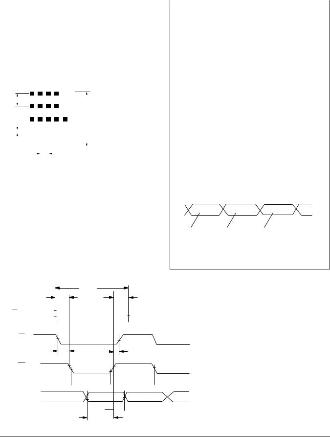
data |
wait |
data |
write control |
wait 130 ns |
write control |
word-clear bit |
|
word-clear bit |
enabled |
|
enabled |
The Flash RAM and Character RAM may not be accessed until the Clear Cycle is complete.
Write Cycle Timing Diagram
Tacc
Tas |
Tah |
FL, A3-A0  see Notes
CE
see Notes
Tces |
Tceh |
WR
see Notes
 Tw
Tw 
 Tbw
Tbw 
D7-D0 |
see Notes |
 Tdh
Tdh 
Tds
Notes
1.All input voltages are (VIL=0.8 V, VIH=2.0 V)
2.These wave forms are not edge triggered.
3.Tbw=Tas + Tah
PLCD5580/1/2/3/4
2–132

Optical Characteristics at 25°C
VCC=5.0 V at Full Brightness
Red PLCD5580
Description |
Symbol |
Min. |
Typ. |
Units |
Peak Luminous Intensity(1) |
IVpeak |
70 |
90 |
cd/dot |
Peak Wavelength |
λ(peak) |
|
660 |
nm |
|
|
|
|
|
Dominant Wavelength |
λ(d) |
|
639 |
nm |
|
|
|
|
|
Yellow PLCD5581 |
|
|
|
|
|
|
|
|
|
Description |
Symbol |
Min. |
Typ. |
Units |
|
|
|
|
|
Peak Luminous Intensity(1) |
IVpeak |
130 |
210 |
cd/dot |
Peak Wavelength |
λ(peak) |
|
583 |
nm |
|
|
|
|
|
Dominant Wavelength |
λ(d) |
|
585 |
nm |
|
|
|
|
|
High Efficiency Red PLCD5582 |
|
|
|
|
|
|
|
|
|
Description |
Symbol |
Min. |
Typ. |
Units |
|
|
|
|
|
Peak Luminous Intensity(1) |
IVpeak |
150 |
330 |
cd/dot |
Peak Wavelength |
λ(peak) |
|
630 |
nm |
|
|
|
|
|
Dominant Wavelength |
λ(d) |
|
626 |
nm |
|
|
|
|
|
Green PLCD5583 |
|
|
|
|
|
|
|
|
|
Description |
Symbol |
Min. |
Typ. |
Units |
|
|
|
|
|
Peak Luminous Intensity(1) |
IVpeak |
150 |
260 |
cd/dot |
Peak Wavelength |
λ(peak) |
|
565 |
nm |
|
|
|
|
|
Dominant Wavelength |
λ(d) |
|
570 |
nm |
|
|
|
|
|
High Efficiency Green PLCD5584 |
|
|
|
|
|
|
|
|
|
Description |
Symbol |
Min. |
Typ. |
Units |
|
|
|
|
|
Peak Luminous Intensity(1) |
IVpeak |
200 |
510 |
cd/dot |
Peak Wavelength |
λ(peak) |
|
568 |
nm |
|
|
|
|
|
Dominant Wavelength |
λ(d) |
|
574 |
nm |
|
|
|
|
|
Note
1. Peak luminous intensity is meaaured at TA=TJ=25°C. No time is allowed for the device to warm up prior to measurement.
PLCD5580/1/2/3/4
2–133

Electrical Characteristics at 25°C
|
|
|
Limits |
|
|
Parameters |
|
|
|
|
Conditions |
|
|
|
|
||
|
Min. |
Typ. |
Max. |
Units |
|
VCC |
4.5 |
5.0 |
5.5 |
V |
|
|
|
|
|
|
|
|
|
|
|
|
|
|
ICC Blank |
|
0.5 |
1.0 |
mA |
VCC=5 V, VIN=5 V |
|||||||||||||
|
|
|
|
|
|
|
||||||||||||
I |
8 digits (1), 16 dots/character |
|
240 |
290 |
mA |
V =5 V, “#” displayed in all |
||||||||||||
CC |
|
|
|
|
|
|
CC |
|||||||||||
|
|
|
|
|
|
eight digits |
||||||||||||
|
|
|
|
|
|
|||||||||||||
IIP Current |
|
11 |
18 |
µA |
VCC=5 V, VIN=0 V to VCC, |
|||||||||||||
(with pull-up) |
|
|
|
|
|
(WR, |
|
CE, |
|
FL, |
|
RST, |
|
ClkSel) |
|
|||
|
|
|
|
|
|
|||||||||||||
II Input leakage current |
|
|
±1 |
µA |
VCC=5 V, VIN=0 V to VCC, |
|||||||||||||
(without pull-up) |
|
|
|
|
(Clk I/O, A0–A3, D0–D7) |
|||||||||||||
|
|
|
|
|
|
|||||||||||||
VIH Input Voltage High |
2.0 |
|
VCC |
V |
VCC=4.5 V to 5.5 V |
|||||||||||||
|
|
|
|
+0.3 |
|
|
|
|
|
|
|
|
|
|
|
|
|
|
|
|
|
|
|
|
|||||||||||||
VIL Input Voltage Low |
GND |
|
0.8 |
V |
VCC=4.5 V to 5.5 V |
|||||||||||||
|
|
–0.3 |
|
|
|
|
|
|
|
|
|
|
|
|
|
|
|
|
|
|
|
|
|
|
|||||||||||||
VOL Output Voltage Low |
|
|
0.4 |
V |
VCC=4.5 V to 5.5 V, |
|||||||||||||
(Clock Pin) |
|
|
|
|
IOL=1.6 mA |
|||||||||||||
VOH Output Voltage High |
2.4 |
|
|
V |
VCC=4.5 V to 5.5 V, |
|||||||||||||
(Clock Pin) |
|
|
|
|
IOH=40 µA |
|||||||||||||
IOH Output Current High |
–0.9 |
|
|
mA |
VCC=4.5 V, VOH=2.4 V |
|||||||||||||
(Clock I/O) |
|
|
|
|
|
|
|
|
|
|
|
|
|
|
|
|
|
|
|
|
|
|
|
|
|||||||||||||
IOL Output Current Low |
1.6 |
2 |
|
mA |
VCC=4.5 V, VOL=0.4 V |
|||||||||||||
(Clock I/O) |
|
|
|
|
|
|
|
|
|
|
|
|
|
|
|
|
|
|
|
|
|
|
|
|
|
|
|
|
|
|
|
|
|
|
|
|
|
θJC Thermal Resistance, |
|
25 |
|
°C/W |
|
|
|
|
|
|
|
|
|
|
|
|
|
|
Junction to Case |
|
|
|
|
|
|
|
|
|
|
|
|
|
|
|
|
|
|
|
|
|
|
|
|
|
|
|||||||||||
Fext External Clock, |
28 |
|
81.14 |
KHz |
VCC=5.0 V, |
|
|
|
|
|
|
|||||||
|
CLKSEL=0 |
|||||||||||||||||
Input Frequency(2) |
|
|
|
|
|
|
|
|
|
|
|
|
|
|
|
|
|
|
Fosc Internal Clock, |
28 |
|
81.14 |
KHz |
VCC=5.0 V, |
|
|
|
|
|
|
|||||||
|
CLKSEL=1 |
|||||||||||||||||
Output Frequency(2) |
|
|
|
|
|
|
|
|
|
|
|
|
|
|
|
|
|
|
Clock I/O Buss Loading |
|
|
240 |
pF |
|
|
|
|
|
|
|
|
|
|
|
|
|
|
|
|
|
|
|
|
|||||||||||||
Clock Out Rise Time |
|
|
500 |
ns |
VCC=4.5 V, VOH=2.4 V |
|||||||||||||
|
|
|
|
|
|
|||||||||||||
Clock Out Fall Time |
|
|
500 |
ns |
VCC=4.5 V, VOL=0.4 V |
|||||||||||||
|
|
|
|
|
|
|
|
|
|
|
|
|
|
|
|
|
|
|
FM, Digit Multiplex Frequency |
125 |
256 |
362.5 |
Hz |
|
|
|
|
|
|
|
|
|
|
|
|
|
|
|
|
|
|
|
|
|
|
|
|
|
|
|
|
|
|
|
|
|
Blinking Rate |
0.98 |
2 |
2.83 |
Hz |
|
|
|
|
|
|
|
|
|
|
|
|
|
|
Notes:
1.Average ICC measured at full brightness. Peak ICC=5⁄8 x IAVG ICC (# displayed).
2.Internal/external frequency duty factor is 50%.
PLCD5580/1/2/3/4
2–134
 Loading...