


ICs for Communications
Quad ISDN Echocancellation Circuit Analogue Front End
Quad IEC AFE
PEB 24902 Version 1.1
PEF 24902 Version 1.1
Data Sheet 5.96
T2490-211-D2-7600

PEB 24902 Revision History |
5.96 |
Previous Releases: 2.96 |
|
p. 21/22 |
PLL characteristics |
|
|
p. 24/25 |
Description of ADC and table 5, ADC |
|
|
p.26 |
Fig. 10 |
|
|
p. 28 |
Description of DAC |
|
|
Edition 5.96
This edition was realized using the software system FrameMakerâ.
Published by Siemens AG, Bereich Halbleiter, MarketingKommunikation, Balanstraße 73, 81541 München
© Siemens AG 1995.
All Rights Reserved.
Attention please!
As far as patents or other rights of third parties are concerned, liability is only assumed for components, not for applications, processes and circuits implemented within components or assemblies.
The information describes the type of component and shall not be considered as assured characteristics.
Terms of delivery and rights to change design reserved.
For questions on technology, delivery and prices please contact the Semiconductor Group Offices in Germany or the Siemens Companies and Representatives worldwide (see address list).
Due to technical requirements components may contain dangerous substances. For information on the types in question please contact your nearest Siemens Office, Semiconductor Group.
Siemens AG is an approved CECC manufacturer.
Packing
Please use the recycling operators known to you. We can also help you – get in touch with your nearest sales office. By agreement we will take packing material back, if it is sorted. You must bear the costs of transport.
For packing material that is returned to us unsorted or which we are not obliged to accept, we shall have to invoice you for any costs incurred.
Components used in life-support devices or systems must be expressly authorized for such purpose!
Critical components1 of the Semiconductor Group of Siemens AG, may only be used in life-support devices or systems2 with the express written approval of the Semiconductor Group of Siemens AG.
1A critical component is a component used in a life-support device or system whose failure can reasonably be expected to cause the failure of that life-support device or system, or to affect its safety or effectiveness of that device or system.
2Life support devices or systems are intended (a) to be implanted in the human body, or (b) to support and/or maintain and sustain human life. If they fail, it is reasonable to assume that the health of the user may be endangered.

|
|
PEB 24902 |
|
|
PEF 24902 |
Table of Contents |
Page |
|
1 |
Overview . . . . . . . . . . . . . . . . . . . . . . . . . . . . . . . . . . . . . . . . . |
. . . . . . . . . .5 |
1.1 |
Features . . . . . . . . . . . . . . . . . . . . . . . . . . . . . . . . . . . . . . . . . |
. . . . . . . . . .6 |
1.2 |
Logic Symbol . . . . . . . . . . . . . . . . . . . . . . . . . . . . . . . . . . . . . . |
. . . . . . . . . .7 |
1.3 |
Functional Block Diagram . . . . . . . . . . . . . . . . . . . . . . . . . . . . |
. . . . . . . . . .8 |
1.4 |
Pin Configuration . . . . . . . . . . . . . . . . . . . . . . . . . . . . . . . . . . . |
. . . . . . . . .9 |
1.5 |
Pin Definitions and Functions . . . . . . . . . . . . . . . . . . . . . . . . . . |
. . . . . . . .10 |
2 |
System Integration . . . . . . . . . . . . . . . . . . . . . . . . . . . . . . . . . . |
. . . . . . . .15 |
2.1 |
Line Card Application . . . . . . . . . . . . . . . . . . . . . . . . . . . . . . . . |
. . . . . . . .15 |
2.2 |
NT Application . . . . . . . . . . . . . . . . . . . . . . . . . . . . . . . . . . . . . . |
. . . . . . . .18 |
3 |
Technical Description . . . . . . . . . . . . . . . . . . . . . . . . . . . . . . . |
. . . . . . . .19 |
3.1 |
Clock Generation . . . . . . . . . . . . . . . . . . . . . . . . . . . . . . . . . . . . |
. . . . . . . .19 |
3.1.1Specification of the PLL and the 15.36 MHz Master Clock (Pin CL15) . . .19
3.1.2 |
Specification of the Crystal . . . . . . . . . . . . . . . . . . . . . . . . . . . . . . . . . . . . |
22 |
3.2 |
Analogue Line Port . . . . . . . . . . . . . . . . . . . . . . . . . . . . . . . . . . . . . . . . . . |
23 |
3.2.1 |
Analogue-to-Digital Converter . . . . . . . . . . . . . . . . . . . . . . . . . . . . . . . . . . |
24 |
3.2.2 |
Range Function . . . . . . . . . . . . . . . . . . . . . . . . . . . . . . . . . . . . . . . . . . . . . |
26 |
3.2.3 |
Digital-to-Analogue Converter . . . . . . . . . . . . . . . . . . . . . . . . . . . . . . . . . . |
26 |
3.2.4 |
External Hybrid and Transformer Parameters . . . . . . . . . . . . . . . . . . . . . . |
29 |
3.2.5 |
Analogue Loop-back Function . . . . . . . . . . . . . . . . . . . . . . . . . . . . . . . . . . |
31 |
3.2.6 |
Level Detect . . . . . . . . . . . . . . . . . . . . . . . . . . . . . . . . . . . . . . . . . . . . . . . . |
32 |
3.2.7 |
Power down . . . . . . . . . . . . . . . . . . . . . . . . . . . . . . . . . . . . . . . . . . . . . . . . |
33 |
3.2.8 |
Power-on-Reset . . . . . . . . . . . . . . . . . . . . . . . . . . . . . . . . . . . . . . . . . . . . . |
33 |
3.2.9 |
Reset . . . . . . . . . . . . . . . . . . . . . . . . . . . . . . . . . . . . . . . . . . . . . . . . . . . . . |
33 |
3.3 |
Digital Interface . . . . . . . . . . . . . . . . . . . . . . . . . . . . . . . . . . . . . . . . . . . . . |
33 |
3.3.1 |
Frame structure on the Digital Interface in the 2B1Q Mode . . . . . . . . . . . |
35 |
3.3.2 |
Frame structure on the Digital Interface in the 4B3T mode . . . . . . . . . . . . |
36 |
3.3.3 |
Propagation Delay in transmit direction . . . . . . . . . . . . . . . . . . . . . . . . . . . |
37 |
3.4 |
NT-Mode Operation . . . . . . . . . . . . . . . . . . . . . . . . . . . . . . . . . . . . . . . . . . |
37 |
3.5 |
Boundary Scan Test Controller . . . . . . . . . . . . . . . . . . . . . . . . . . . . . . . . . |
39 |
4 |
Digital Interface. . . . . . . . . . . . . . . . . . . . . . . . . . . . . . . . . . . . . . . . . . . . . |
42 |
4.1 |
Static Requirements . . . . . . . . . . . . . . . . . . . . . . . . . . . . . . . . . . . . . . . . . |
42 |
4.2 |
Dynamic Requirements . . . . . . . . . . . . . . . . . . . . . . . . . . . . . . . . . . . . . . . |
43 |
4.3 |
Boundary Scan Timing . . . . . . . . . . . . . . . . . . . . . . . . . . . . . . . . . . . . . . . |
44 |
5 |
Power Supply . . . . . . . . . . . . . . . . . . . . . . . . . . . . . . . . . . . . . . . . . . . . . . |
46 |
5.1 |
Supply Voltages . . . . . . . . . . . . . . . . . . . . . . . . . . . . . . . . . . . . . . . . . . . . . |
46 |
5.2 |
Power Consumption . . . . . . . . . . . . . . . . . . . . . . . . . . . . . . . . . . . . . . . . . |
46 |
6 |
Maximum ratings . . . . . . . . . . . . . . . . . . . . . . . . . . . . . . . . . . . . . . . . . . . |
47 |
6.1 |
Line Overload Protection . . . . . . . . . . . . . . . . . . . . . . . . . . . . . . . . . . . . . . |
47 |
Semiconductor Group |
3 |
05.96 |

|
|
PEB 24902 |
|
|
PEF 24902 |
Table of Contents |
Page |
|
7 |
Environmental Requirements . . . . . . . . . . . . . . . . . . . . . . . . |
. . . . . . . . .49 |
7.1 |
Storage and Transportation . . . . . . . . . . . . . . . . . . . . . . . . . . . |
. . . . . . . . .49 |
7.2 |
Operating Ambient . . . . . . . . . . . . . . . . . . . . . . . . . . . . . . . . . . . |
. . . . . . . .49 |
7.3 |
Thermal Contact Resitance . . . . . . . . . . . . . . . . . . . . . . . . . . . . |
. . . . . . . .49 |
8 |
Package Outlines . . . . . . . . . . . . . . . . . . . . . . . . . . . . . . . . . . . |
. . . . . . . .50 |
Semiconductor Group |
4 |
05.96 |

PEB 24902
PEF 24902
Overview
1 Overview
The PEB 24902 Quad IEC AFE (Quadruple ISDN Echocancellation Circuit Analogue Front End) is part of a 2B1Q or 4B3T ISDN U-transceiver chip set. Up to four lines can be accessed simultaneously by the Quad IEC AFE. The Quad IEC AFE is optimized to work in conjunction with the PEB 24901 Quad IEC DFE-T and the PEB 24911 Quad IEC DFE-Q. An integrated PLL synchronizes the 15.36 MHz Master clock onto the 8 kHz or 2048 kHz PTT Clock. This specification describes the functionality for 2B1Q and 4B3T interfaces.
Semiconductor Group |
5 |
05.96 |

Quad ISDN Echocancellation Circuit Analogue Front End |
PEB 24902 |
Quad IEC AFE |
PEF 24902 |
Version 1.1 |
CMOS |
1.1Features
•Digital to Analogue conversion (transmit pulse)
•Output buffering
• Analogue to digital conversion
•Detection of signal on the line
•Master clock generation by PLL
•P-MQFP-64 Package
• |
Compliant to ANSI T1.601 (1992), ETSI ETR 080 |
P-MQFP-64-1 |
|
(1995) |
|
|
|
|
• |
JTAG boundary scan path compliant to IEEE 1149.1 |
|
Semiconductor Group |
6 |
05.96 |
PEB 24902
PEF 24902
Overview
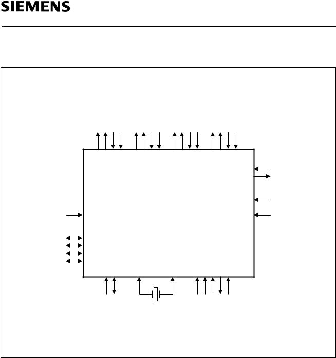
1.2Logic Symbol
Analog Line Ports
BIN1
AIN1
BOUT1
AOUT1
+5 V  V DD d1...2, a1...4 0 V
  GNDd1...2, a1...4
 CODE
CODE
Mode Settings  ADDR
ADDR
PLLF
 RES
RES
|
|
V REF1 |
|
|
|
|
|
Block Capacitors |
|
V REF2 |
|
|
|
||
100 nF to GND |
|
V REF3 |
CLOCK CL15 |
|
|||
|
|
V REF4 |
|
|
|
|
AOUT2 BOUT2 AIN2 BIN2 |
AOUT3 BOUT3 AIN3 BIN3 |
PEB 24902
AOUT4 BOUT4 |
AIN4 BIN4 |
|
SDX |
|
SDR |
XDN1
XDN2
XDN3
XDN4
PDM1 
PDM2 
PDM3 
PDM4 
XIN |
XOUT |
TMS TCK TDI TDO |
|
TDISS |
|
Boundary Scan Pins
Serial Interface to PEB 24901 or PEB 24911
Transmit Data from PEB 24911 in NT Mode
ADC Outputs
ITL07131
Figure 1
Logic Symbol
Semiconductor Group |
7 |
05.96 |

PEB 24902
PEF 24902
Overview
1.3Functional Block Diagram
DFE |
Digital |
D |
|
|
Buffer |
|
Interface |
Interface |
|
|
A |
||
|
|
|
|
|||
|
|
|
Level |
|
A |
D |
|
|
|
|
|
||
|
|
|
|
|
|
|
|
|
|
Voltage Reference |
|
||
|
Common |
|
|
|
|
|
|
PLL |
|
|
|
|
|
|
|
D |
|
A |
Buffer |
|
|
|
|
|
|
||
|
|
|
|
|
|
|
|
|
|
Level |
|
A |
D |
|
|
|
|
|
||
|
|
|
|
|
|
|
|
|
|
Voltage Reference |
|
||
Trafo Analogue
Hybrid IN/OUT
Trafo Analogue
Hybrid IN/OUT
ITB07132
Figure 2
Block Diagram of the Quad IEC AFE
Semiconductor Group |
8 |
05.96 |
PEB 24902
PEF 24902
Overview
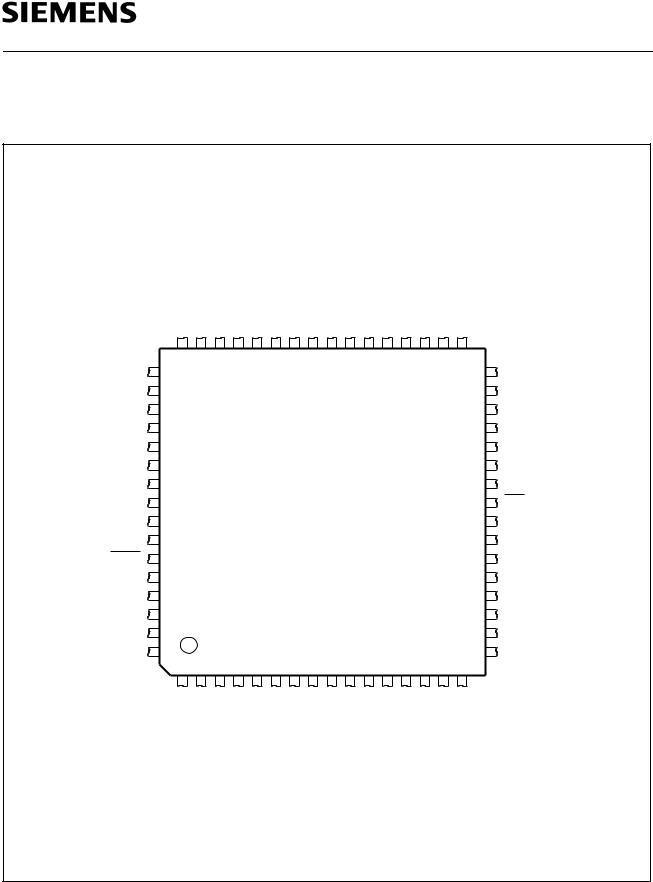
1.4Pin Configuration
N.C. AOUT3 V |
N.C. BOUT3 N.C. V |
SDR PDM3 PDM2 PDM1 V |
BOUT1 N.C. V |
AOUT1 |
DD |
SS |
DD |
DD |
|
VSS |
48 |
47 |
46 |
45 |
44 |
43 |
42 |
41 40 |
39 |
38 |
37 |
36 |
35 |
34 |
33 |
|
49 |
|
|
|
|
|
|
|
|
|
|
|
|
|
|
32 |
|
XDN3 |
50 |
|
|
|
|
|
|
|
|
|
|
|
|
|
|
31 |
VREF3 |
51 |
|
|
|
|
|
|
|
|
|
|
|
|
|
|
30 |
AIN3 |
52 |
|
|
|
|
|
|
|
|
|
|
|
|
|
|
29 |
BIN3 |
53 |
|
|
|
|
|
|
|
|
|
|
|
|
|
|
28 |
N.C. |
54 |
|
|
|
|
|
|
|
|
|
|
|
|
|
|
27 |
TDI |
55 |
|
|
|
|
|
|
|
|
|
|
|
|
|
|
26 |
TDO |
56 |
|
|
|
|
|
PEB 24902 |
|
|
|
|
|
25 |
|||
TCK |
57 |
|
|
|
|
|
|
|
|
|
|
24 |
||||
|
|
|
|
|
|
|
|
|
|
|
|
|
|
|||
TMS |
58 |
|
|
|
|
|
|
|
|
|
|
|
|
|
|
23 |
TDISS |
59 |
|
|
|
|
|
|
|
|
|
|
|
|
|
|
22 |
BIN4 |
60 |
|
|
|
|
|
|
|
|
|
|
|
|
|
|
21 |
AIN4 |
61 |
|
|
|
|
|
|
|
|
|
|
|
|
|
|
20 |
VREF4 |
62 |
|
|
|
|
|
|
|
|
|
|
|
|
|
|
19 |
XDN4 |
63 |
|
|
|
|
|
|
|
|
|
|
|
|
|
|
18 |
VSS |
64 |
2 |
3 |
4 |
5 |
6 |
7 |
8 |
9 |
10 |
11 12 |
13 |
14 |
15 |
17 |
|
|
1 |
16 |
||||||||||||||
|
N.C. |
AOUT4 |
DD |
N.C. |
BOUT4 |
SS |
CL15 |
PDM4 |
XOUT |
XIN |
DD |
N.C. |
BOUT2 |
N.C. |
DD |
AOUT2 |
|
V |
V |
V |
V |
||||||||||||
VSS
XDN1
VREF1
AIN1
BIN1
ADDR CLOCK
RES
SDX
CODE
PLLF
BIN2
AIN2
VREF2
XDN2
VSS
ITP07133
Figure 3
Pin Configuration
(top view)
Semiconductor Group |
9 |
05.96 |

PEB 24902
PEF 24902
Overview
1.5Pin Definitions and Functions
The following tables group the pins according to their functions. They include pin name, pin number, type, a brief description of the function and cross-references referring to the sections in which the pin functions are discussed.
Table 1
Pin Definitions and Functions
Pin No. |
Symbol |
Input (I) |
Description |
Reference |
|
|
Output (O) |
|
|
|
|
|
|
|
Power Supply Pins |
|
|
|
|
|
|
|
|
|
37 |
VDDd1 |
|
5V +/-5% digital supply voltage |
5.1 |
11 |
VDDd2 |
|
|
|
34 |
VDDa1 |
|
5V +/-5% analogue supply voltage |
5.1 |
15 |
VDDa2 |
|
|
|
46 |
VDDa3 |
|
|
|
3 |
VDDa4 |
|
|
|
42 |
GNDd1 |
|
0V digital |
5.1 |
6 |
GNDd2 |
|
|
|
32 |
GNDa1 |
|
0V analogue |
5.1 |
17 |
GNDa2 |
|
|
|
49 |
GNDa3 |
|
|
|
64 |
GNDa4 |
|
|
|
30 |
VREF1 |
I/O |
VREF pin to Buffer internally |
2 |
|
|
|
generated voltage with capacitor |
|
|
|
|
100 nF vs. GND |
|
|
|
|
|
|
19 |
VREF2 |
I/O |
VREF pin to Buffer internally |
2 |
|
|
|
generated voltage with capacitor |
|
|
|
|
100 nF vs. GND |
|
|
|
|
|
|
51 |
VREF3 |
I/O |
VREF pin to Buffer internally |
2 |
|
|
|
generated voltage with capacitor |
|
|
|
|
100 nF vs. GND |
|
|
|
|
|
|
Semiconductor Group |
10 |
05.96 |
PEB 24902
PEF 24902
Overview
Table 1
Pin Definitions and Functions (cont’d)
Pin No. |
|
Symbol |
Input (I) |
Description |
Reference |
|
|
|
|
|
Output (O) |
|
|
|
|
|
|
|
|
|
62 |
|
VREF4 |
I/O |
VREF pin to Buffer internally |
2 |
|
|
|
|
|
|
generated voltage with capacitor. |
|
|
|
|
|
|
100 nF vs. GND |
|
|
|
|
|
|
||
JTAG Boundary Scan |
|
|
||||
|
|
|
|
|
|
|
57 |
|
TCK |
I |
Test Clock. |
3.5,4.3 |
|
|
|
|
|
|
|
|
58 |
|
TMS |
I |
Test Mode Select, internal pullup. |
3.5,4.3 |
|
|
|
|
|
|
|
|
55 |
|
TDI |
I |
Test Data Input, internal pullup. |
3.5,4.3 |
|
|
|
|
|
|
|
|
56 |
|
TDO |
O |
Test Data Output. |
3.5,4.3 |
|
|
|
|
|
|
|
|
59 |
|
|
|
I |
JTAG Boundary Scan Disable, active |
3.5 |
TDISS |
||||||
|
|
|
|
|
low, internal pullup. |
|
|
|
|
|
|
||
Line Port Pins |
|
|
|
|||
|
|
|
|
|
|
|
29 |
|
AIN1 |
I |
Differential U interface input. |
3.2.1 |
|
|
|
|
|
|
Line port 1 |
|
|
|
|
|
|
|
|
28 |
|
BIN1 |
I |
Differential U interface input. |
3.2.1 |
|
|
|
|
|
|
Line port 1 |
|
|
|
|
|
|
|
|
33 |
|
AOUT1 |
O |
Differential U interface output. |
3.2.3 |
|
|
|
|
|
|
Line port 1 |
|
|
|
|
|
|
|
|
36 |
|
BOUT1 |
O |
Differential U interface output. |
3.2.3 |
|
|
|
|
|
|
Line port 1 |
|
|
|
|
|
|
|
|
20 |
|
AIN2 |
I |
Differential U interface input. |
3.2.1 |
|
|
|
|
|
|
Line port 2 |
|
|
|
|
|
|
|
|
21 |
|
BIN2 |
I |
Differential U interface input. |
3.2.1 |
|
|
|
|
|
|
Line port 2 |
|
|
|
|
|
|
|
|
16 |
|
AOUT2 |
O |
Differential U interface output. |
3.2.3 |
|
|
|
|
|
|
Line port 2 |
|
|
|
|
|
|
|
|
13 |
|
BOUT2 |
O |
Differential U interface output. |
3.2.3 |
|
|
|
|
|
|
Line port 2 |
|
|
|
|
|
|
|
|
52 |
|
AIN3 |
I |
Differential U interface input. |
3.2.1 |
|
|
|
|
|
|
Line port 3 |
|
|
|
|
|
|
|
|
Semiconductor Group |
11 |
05.96 |

PEB 24902
PEF 24902
Overview
Table 1
Pin Definitions and Functions (cont’d)
Pin No. |
Symbol |
Input (I) |
Description |
Reference |
|
|
Output (O) |
|
|
|
|
|
|
|
53 |
BIN3 |
I |
Differential U interface input. |
3.2.1 |
|
|
|
Line port 3 |
|
|
|
|
|
|
47 |
AOUT3 |
O |
Differential U interface output. |
3.2.3 |
|
|
|
Line port 3 |
|
|
|
|
|
|
44 |
BOUT3 |
O |
Differential U interface output. |
3.2.3 |
|
|
|
Line port 3 |
|
|
|
|
|
|
61 |
AIN4 |
I |
Differential U interface input. |
3.2.1 |
|
|
|
Line port 4 |
|
|
|
|
|
|
60 |
BIN4 |
I |
Differential U interface input. |
3.2.1 |
|
|
|
Line port 4 |
|
|
|
|
|
|
2 |
AOUT4 |
O |
Differential U interface output. |
3.2.3 |
|
|
|
Line port 4 |
|
|
|
|
|
|
5 |
BOUT4 |
O |
Differential U interface output. |
3.2.3 |
|
|
|
Line port 4 |
|
|
|
|
|
|
Digital Interface |
|
|
|
|
|
|
|
|
|
7 |
CL15 |
I/O |
Master Clock 15.36 MHz. All |
3.1.1, 4.2 |
|
|
|
operations and the data exchange on |
|
|
|
|
the digital interface are based on this |
|
|
|
|
clock. If a 15.36 MHz clock is |
|
|
|
|
generated by the internal PLL/ |
|
|
|
|
oscillator or if an external clock is |
|
|
|
|
provided at XIN then CL15 issues this |
|
|
|
|
clock. If the pin XIN is clamped to low |
|
|
|
|
or high then CL15 is input and an |
|
|
|
|
other device has to provide the 15.36 |
|
|
|
|
MHz clock. |
|
|
|
|
|
|
38 |
PDM1 |
O |
Pulse density modulated output of the |
3.2.1, 4.2 |
|
|
|
second-order sigma-delta ADC of line |
|
|
|
|
port 1 |
|
|
|
|
|
|
39 |
PDM2 |
O |
Pulse density modulated output of the |
3.2.1, 4.2 |
|
|
|
second-order sigma-delta ADC of line |
|
|
|
|
port 2 |
|
|
|
|
|
|
Semiconductor Group |
12 |
05.96 |

PEB 24902
PEF 24902
Overview
Table 1
Pin Definitions and Functions (cont’d)
Pin No. |
Symbol |
Input (I) |
Description |
Reference |
|
|
Output (O) |
|
|
|
|
|
|
|
40 |
PDM3 |
O |
Pulse density modulated output of the |
3.2.1, 4.2 |
|
|
|
second-order sigma-delta ADC of line |
|
|
|
|
port 3 |
|
|
|
|
|
|
8 |
PDM4 |
O |
Pulse density modulated output of the |
3.2.1, 4.2 |
|
|
|
second-order sigma-delta ADC of line |
|
|
|
|
port 4. |
|
|
|
|
|
|
31 |
XDN1 |
I |
Input for Transmit data in NT mode. |
3.4 |
|
|
|
Not used in LT-Mode. Internal |
|
|
|
|
pulldown. |
|
|
|
|
|
|
18 |
XDN2 |
I |
Input for Transmit data in NT mode. |
3.4 |
|
|
|
Not used in LT-Mode. Internal |
|
|
|
|
pulldown. |
|
|
|
|
|
|
50 |
XDN3 |
I |
Input for Transmit data in NT mode. |
3.4 |
|
|
|
Not used in LT-Mode. Internal |
|
|
|
|
pulldown. |
|
|
|
|
|
|
63 |
XDN4 |
I |
Input for Transmit data in NT mode. |
3.4 |
|
|
|
Not used in LT-Mode. Internal |
|
|
|
|
pulldown. |
|
|
|
|
|
|
24 |
SDX |
I |
Interface for the transmit and control |
3.3, 4.2 |
|
|
|
data. Up to eight lines can be |
|
|
|
|
multiplexed on SDX. Transmission |
|
|
|
|
and sampling is based on clock CL15 |
|
|
|
|
(15,36 MBit/sec): |
|
|
|
|
For each line port the following bits |
|
|
|
|
are exchanged: |
|
|
|
|
TD0, TD1, TD2: Transmit data |
|
|
|
|
RANGE: Range select |
|
|
|
|
LOOP: Analogue loop back switch |
|
|
|
|
PDOW: Power down/power up |
|
|
|
|
NT: NT-Mode or LT-Mode |
|
|
|
|
Synchronization information |
|
|
|
|
|
|
41 |
SDR |
O |
Level information for the detection of |
3.3, 4.2 |
|
|
|
the awake tone. The four lines are |
|
|
|
|
multiplexed on SDR. |
|
|
|
|
|
|
Semiconductor Group |
13 |
05.96 |

PEB 24902
PEF 24902
Overview
Table 1
Pin Definitions and Functions (cont’d)
Pin No. |
Symbol |
Input (I) |
Description |
Reference |
||
|
|
|
|
Output (O) |
|
|
|
|
|
|
|
||
27 |
ADDR |
I |
Select the assignment of time slots |
3.3 |
||
|
|
|
|
|
and line ports. |
|
|
|
|
|
|
|
|
23 |
|
CODE |
I |
Select 2B1Q or 4B3T code. Code = |
3.3, 3.2.3 |
|
|
|
|
|
|
low sets 2B1Q Code. |
|
|
|
|
|
|
|
|
25 |
|
|
|
I |
Reset and power down of the entire |
3.2.9 |
RES |
||||||
|
|
|
|
|
IEC Quad AFE including PLL and all |
|
|
|
|
|
|
four line ports. Asynchronous signal, |
|
|
|
|
|
|
active low. |
|
|
|
|
|
|
|
|
PLL |
|
|
|
|
|
|
|
|
|
|
|
||
9 |
XOUT |
O |
Crystal out. 15.36 MHz crystal is |
3.1.2 |
||
|
|
|
|
|
connected. Leave open if not used. |
|
|
|
|
|
|
||
10 |
XIN |
I |
Crystal in. External 15.36 MHz clock |
3.1, 3.1.2 |
||
|
|
|
|
|
signal or 15.36 MHz crystal is |
|
|
|
|
|
|
connected. Clamping XIN to either low |
|
|
|
|
|
|
or high sets CL15 to Input. |
|
|
|
|
|
|
||
26 |
CLOCK |
I |
8 kHz or 2048 kHz clock as a time |
3.1 |
||
|
|
|
|
|
base of the 15.36 MHz clock.Connect |
|
|
|
|
|
|
to GND if not used. |
|
|
|
|
|
|
|
|
22 |
|
PLLF |
I |
Select corner frequency of PLL Jitter |
3.1 |
|
|
|
|
|
|
Transfer function. Internal pullup |
|
|
|
|
|
|
resistor. |
|
|
|
|
|
|
|
|
Semiconductor Group |
14 |
05.96 |

PEB 24902
PEF 24902
System Integration
2 System Integration
The Quad IEC AFE is optimized for line modules in the central office or access networks (LT function) together with the PEB 24901 Quad IEC DFE-T for 4B3T code or the PEB 24911 Quad IEC DFE-Q for 2B1Q code. Application in the multi channel NT function together with the PEB 24911 Quad IEC DFE-Q V2.1 is supported. The PEB 24911 Quad IEC DFE-Q is footprint compatible to the PEB 24901 Quad IEC DFE-T. This way, one board layout can be used for both line codes simply by putting the appropriate DFE.
2.1Line Card Application
The Quad IEC AFE is controlled via the signal at pin SDX. The transmit data is transferred the same way. Data on SDX is organized such that two Quad IEC AFE devices can share the same signal.
The Quad IEC AFE can transmit either 2B1Q-data or 4B3T-data. Setting the pin CODE to low will result in 2B1Q code. For 4B3T code the pin CODE has to be tied to VDD.
Each of the four line ports is biased by a separate voltage reference. This internal reference voltage has to be decoupled by a capacitor of 100 nF connected to the VREFx pin and GND.
The 15.36 MHz master clock is generated with a crystal oscillator and synchronized onto the PTT clock with an integrated PLL. Fig. 4 shows a 4 channel LT application for 2B1Q line code. Note, that the PEB 24911 Quad IEC DFE-Q is footprint compatible to the PEB 24901 Quad IEC DFE-T. This way, one board layout can be used for both linecodes simply by putting the appropriate DFE.
Figure 4
4 channel LT application
Semiconductor Group |
15 |
05.96 |
 Loading...