


Quad Driver Incl. Short-Circuit Signaling |
FZL 4145 D |
Bipolar IC
Features
● Short-circuit shutdown with clock generator ● Four driver circuits for controlling
power transistors
● Overload and short-circuit signaling
P-DIP-18-1
Type |
Ordering Code |
Package |
|
|
|
FZL 4145 D |
Q67000-H8437 |
P-DIP-18-1 |
|
|
|
General Description
The IC comprises four driver circuits capable of driving power transistors for high output currents. The output transistors are protected against short-circuit to ground and supply voltage. The input threshold can be adjusted between 1.5 V and 7 V. Overload or shortcircuit failure at an output will be indicated at pin SQ (signaling output).
Functional Description
Each driver circuit has one active high driver input Dl and a common enable input (ENA) (active high) is provided for all stages. The (Q) outputs are designed to drive the output transistors. The load current is sampled via pin W. If the load current exceeds the preset value, the output stage switches off. Switching-on again is provided by the built-in clock generator. Its operation requires an external capacitor CT at pin C. If CT is bridged by a break-key, switching on can only be carried out by operating a key. The duty cycle of the clock generator is 1:50 (e.g. 40 μs/2 ms with CT = 33 nF).
In case of overcurrent or short-circuit failure at any output stage the signaling output (SQ) will go low. In clock-governed operation (i.e. when there is automatic switching on by the clock and not by a key), SQ goes high and low at the clock rate as long as a shortcircuit or overload exists. SQ is an open-collector output.
Unused W pins must be connected to Vs. Open W pins would simulate a short-circuit and activate the signaling output.
Semiconductor Group |
1 |
09.94 |
FZL 4145 D
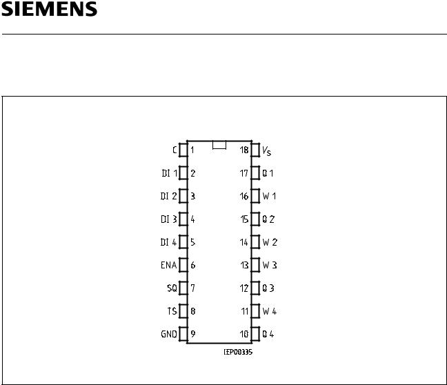
Pin Configuration
(top view)
Semiconductor Group |
2 |

FZL 4145 D
DI |
Driver inputs |
ENA |
Enable input |
C |
Clock capacitor |
Q |
Outputs |
TS |
Input for threshold switching |
W |
Input for output current limiter |
SQ |
Signaling output |
GND |
Ground |
Block Diagram
The switching threshold at inputs Dl and ENA can be adjusted between 1.5 V and 7 V via connection TS:
VTS = 0 V; |
input threshold = 1.5 V (for 5 V logic) |
VTS = 0 to 5 V; |
input threshold = VTS + 1.5 V |
VTS = VS: |
input threshold = 7 V (for 12/15 V and 24/28 V logic) |
If the output is disabled due to the logic states of inputs Dl or ENA this disable is effective over the total supply voltage range between VS = 0 V and VS = 35 V.
The inputs are protected with clamp diodes.
Semiconductor Group |
3 |
 Loading...