


 Loading...
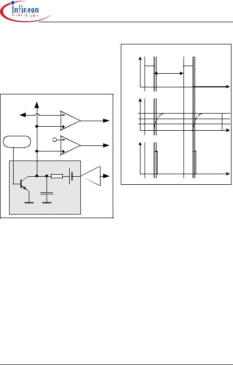
INFINEON ICE2A0565, ICE2A165, ICE2A265, ICE2A365, ICE2B0565 User Manual
...Datasheet V4.5, Jan 2004
CoolSET™-F2
I C E 2 A 0 5 6 5 / 1 6 5 / 2 6 5 / 3 6 5 I C E 2 B 0 5 6 5 / 1 6 5 / 2 6 5 / 3 6 5 I C E 2 A 0 5 6 5 Z
I C E 2 A 1 8 0 Z / 2 8 0 Z
I C E 2 A 7 6 5 I / 2 B 7 6 5 I
I C E 2 A 7 6 5 P 2 / I C E 2 B 7 6 5 P 2
Off-Line SMPS Current Mode Controller with integrated 650V/800V CoolMOS™
P o w e r M a n a g e m e n t & S u p p l y
N e v e r s t o p t h i n k i n g .

CoolSET™-F2 |
|
|
|
Revision History: |
2004-01-28 |
Datasheet V4.5 |
|
|
|
|
|
Previous Version: |
|
|
|
|
|
|
|
Page |
Subjects (major changes since last revision) |
|
|
|
|
|
|
|
|
|
|
|
|
|
|
|
|
|
|
|
|
|
|
|
|
|
|
For questions on technology, delivery and prices please contact the Infineon Technologies Offices in Germany or the Infineon Technologies Companies and Representatives worldwide: see our webpage at http:// www.infineon.com.
CoolMOS™, CoolSET™ are trademarks of Infineon Technologies AG.
Edition 2004-01-28
Published by Infineon Technologies AG, St.-Martin-Strasse 53,
D-81541 München
© Infineon Technologies AG 1999. All Rights Reserved.
Attention please!
The information herein is given to describe certain components and shall not be considered as warranted characteristics.
Terms of delivery and rights to technical change reserved.
We hereby disclaim any and all warranties, including but not limited to warranties of non-infringement, regarding circuits, descriptions and charts stated herein.
Infineon Technologies is an approved CECC manufacturer.
Information
For further information on technology, delivery terms and conditions and prices please contact your nearest Infineon Technologies Office in Germany or our Infineon Technologies Representatives worldwide (see address list).
Warnings
Due to technical requirements components may contain dangerous substances. For information on the types in question please contact your nearest Infineon Technologies Office.
Infineon Technologies Components may only be used in life-support devices or systems with the express written approval of Infineon Technologies, if a failure of such components can reasonably be expected to cause the failure of that life-support device or system, or to affect the safety or effectiveness of that device or system. Life support devices or systems are intended to be implanted in the human body, or to support and/or maintain and sustain and/or protect human life. If they fail, it is reasonable to assume that the health of the user or other persons may be endangered.
Off-Line SMPS Current Mode Controller
with integrated |
650V/800V |
Product Highlights
•Best in class in DIP8, DIP7, TO220 packages
•No heatsink required for DIP8, DIP7
•Lowest standby power dissipation
•Enhanced protection functions all with Auto Restart Mode
•Isolated drain package for TO220
•Increased creepage distance for TO220 packages
CoolSET™-F2 |
P-DIP-7-1 |
P-DIP-7-1 |
P-DIP-8-6 |
P-DIP-8-4, -6 |
PP--TO220O220-6-46-6-46 P-TO220-6-47 |
P-TO220-6-47 |
Features |
Description |
|
• 650V/800V avalanche rugged CoolMOS™ |
The second generation CoolSET™-F2 provides several |
|
• Only few external components required |
special enhancements to satisfy the needs for low power |
|
• Input Vcc Undervoltage Lockout |
standby and protection features. In standby mode |
|
• |
67kHz/100kHz switching frequency |
frequency reduction is used to lower the power |
• Max duty cycle 72% |
consumption and support a stable output voltage in this |
|
• Low Power Standby Mode to meet |
mode. The frequency reduction is limited to 20kHz/21.5 |
|
|
European Commission Requirements |
kHz to avoid audible noise. In case of failure modes like |
• Thermal Shut Down with Auto Restart |
open loop, overvoltage or overload due to short circuit the |
|
• Overload and Open Loop Protection |
device switches in Auto Restart Mode which is controlled by |
|
• Overvoltage Protection during Auto Restart |
the internal protection unit. By means of the internal precise |
|
• Adjustable Peak Current Limitation via |
peak current limitation the dimension of the transformer and |
|
|
external resistor |
the secondary diode can be lower which leads to more cost |
• |
Overall tolerance of Current Limiting < ±5% |
efficiency. |
•Internal Leading Edge Blanking
•User defined Soft Start Soft Switching for low EMI
|
|
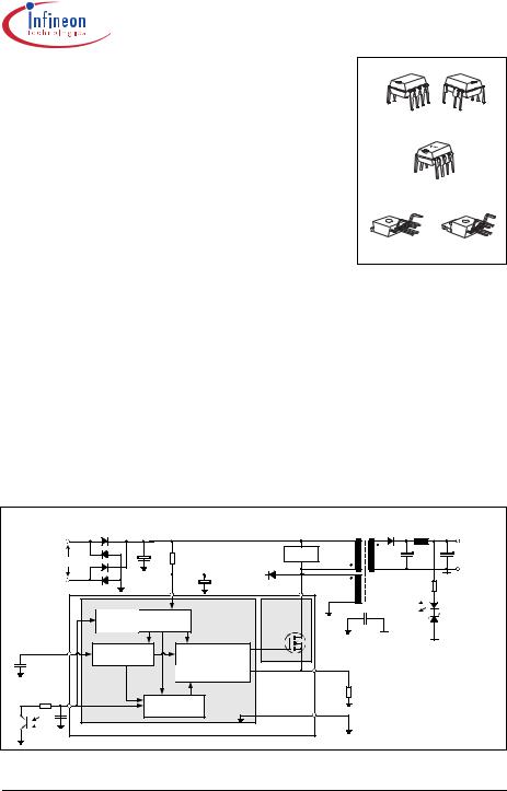
Typical Application |
|
|
|
|
|
|
+ |
|
|
RStart-up |
Snubber |
Converter |
85 ... 270 VAC |
|
DC Output |
||
|
|
|||
|
|
|
|
- |
|
|
CVCC |
Drain |
|
|
|
VCC |
|
|
|
|
|
|
Feedback |
Low Power |
|
Power |
|
|
StandBy |
Management |
CoolMOS™ |
|
|
|
|
|
|
|
SoftS |
|
PWM Controller |
|
|
Soft-Start Control |
|
|
||
Current Mode |
|
|
||
CSoft Start |
|
|
|
|
|
Precise Low Tolerance |
|
Isense |
|
|
|
Peak Current Limitation |
|
|
FB |
|
|
|
RSense |
|
Protection Unit |
|
|
|
|
|
|
GND |
|
PWM-Controller |
|
|
|
|
|
|
|
|
|
CoolSET™-F2 |
|
|
|
|
Feedback |
|
|
|
|
Datasheet V4.5 |
|
3 |
|
Jan 2004 |

CoolSET™-F2
Ordering Codes
Type |
Ordering Code |
Package |
VDS |
FOSC |
RDSon1) |
230VAC ±15% 2) |
85-265 VAC2) |
ICE2A0565 |
Q67040-S4542 |
P-DIP-8-6 |
650V |
100kHz |
4.7Ω |
23W |
13W |
ICE2A165 |
Q67040-S4426 |
P-DIP-8-6 |
650V |
100kHz |
3.0Ω |
31W |
18W |
ICE2A265 |
Q67040-S4414 |
P-DIP-8-6 |
650V |
100kHz |
0.9Ω |
52W |
32W |
ICE2A365 |
Q67040-S4415 |
P-DIP-8-6 |
650V |
100kHz |
0.45Ω |
67W |
45W |
ICE2B0565 |
Q67040-S4540 |
P-DIP-8-6 |
650V |
67kHz |
4.7Ω |
23W |
13W |
ICE2B165 |
Q67040-S4489 |
P-DIP-8-6 |
650V |
67kHz |
3.0Ω |
31W |
18W |
ICE2B265 |
Q67040-S4478 |
P-DIP-8-6 |
650V |
67kHz |
0.9Ω |
52W |
32W |
ICE2B365 |
Q67040-S4490 |
P-DIP-8-6 |
650V |
67kHz |
0.45Ω |
67W |
45W |
ICE2A0565Z |
Q67040-S4541 |
P-DIP-7-1 |
650V |
100kHz |
4.7Ω |
23W |
13W |
ICE2A180Z |
Q67040-S4546 |
P-DIP-7-1 |
800V |
100kHz |
3.0Ω |
29W |
17W |
ICE2A280Z |
Q67040-84547 |
P-DIP-7-1 |
800V |
100KHz |
0.8Ω |
50W |
31W |
|
|
|
|
|
|
|
|
1)typ @ T=25°C
2)Maximum power rating at Ta=75°C, Tj=125°C and with copper area on PCB = 6cm²
Type |
Ordering Code |
Package |
VDS |
FOSC |
RDSon1) |
230VAC ±15% 2) |
85-265 VAC2) |
ICE2A765I |
Q67040-S4609 |
P-TO-220-6-46 |
650V |
100kHz |
0.45Ω |
240W |
130W |
ICE2B765I |
Q67040-S4607 |
P-TO-220-6-46 |
650V |
67kHz |
0.45Ω |
240W |
130W |
ICE2A765P2 |
Q67040-S4610 |
P-TO-220-6-47 |
650V |
100kHz |
0.45Ω |
240W |
130W |
ICE2B765P2 |
Q67040-S4608 |
P-TO-220-6-47 |
650V |
67kHz |
0.45Ω |
240W |
130W |
|
|
|
|
|
|
|
|
1)typ @ T=25°C
2)Maximum practical continuous power in an open frame design at Ta=75°C, Tj=125°C and Rth=2.7K/W
Datasheet V4.5 |
4 |
Jan 2004 |

CoolSET™-F2
Table of Contents |
|
Page |
||
1 |
Pin Configuration and Functionality . . . . . . . . . . . . . . . . . . . . . . . |
. . . . . .6 |
|
|
1.1 |
Pin Configuration with P-DIP-8-6 |
. . . . . . . . . . . . . . . . . . . . . . . . . . . . |
. . . . . .6 |
|
1.2 |
Pin Configuration with P-DIP-7-1 |
. . . . . . . . . . . . . . . . . . . . . . . . . . . . |
. . . . . .6 |
|
1.3 |
Pin Configuration with P-TO220-6-46/47 . . . . . . . . . . . . . . . . . . . . . . |
. . . . . .7 |
||
1.4 |
Pin Functionality . . . . . . . . . . . . |
. . . . . . . . . . . . . . . . . . . . . . . . . . . . |
. . . . . .7 |
|
2 |
Representative Blockdiagram |
. . . . . . . . . . . . . . . . . . . . . . . . . . . . |
. . . . . .8 |
|
3 |
Functional Description . . . . . . |
. . . . . . . . . . . . . . . . . . . . . . . . . . . . |
. . . . . .9 |
|
3.1 |
Power Management . . . . . . . . . . |
. . . . . . . . . . . . . . . . . . . . . . . . . . . . |
. . . . . .9 |
|
3.2 |
Improved Current Mode . . . . . . . |
. . . . . . . . . . . . . . . . . . . . . . . . . . . . |
. . . . . .9 |
|
3.2.1 |
PWM-OP . . . . . . . . . . . . . . . . |
. . . . . . . . . . . . . . . . . . . . . . . . . . . . |
. . . . .10 |
|
3.2.2 |
PWM-Comparator . . . . . . . . . |
. . . . . . . . . . . . . . . . . . . . . . . . . . . . |
. . . . .10 |
|
3.3 |
Soft-Start . . . . . . . . . . . . . . . . . . |
. . . . . . . . . . . . . . . . . . . . . . . . . . . . |
. . . . .11 |
|
3.4 |
Oscillator and Frequency Reduction . . . . . . . . . . . . . . . . . . . . . . . . . |
. . . . .12 |
|
|
3.4.1 |
Oscillator . . . . . . . . . . . . . . . . |
. . . . . . . . . . . . . . . . . . . . . . . . . . . . |
. . . . .12 |
|
3.4.2 |
Frequency Reduction . . . . . . . |
. . . . . . . . . . . . . . . . . . . . . . . . . . . . |
. . . . .12 |
|
3.5 |
Current Limiting . . . . . . . . . . . . . |
. . . . . . . . . . . . . . . . . . . . . . . . . . . . |
. . . . .12 |
|
3.5.1 |
Leading Edge Blanking . . . . . |
. . . . . . . . . . . . . . . . . . . . . . . . . . . . . |
. . . .12 |
|
3.5.2 |
Propagation Delay Compensation . . . . . . . . . . . . . . . . . . . . . . . . . . |
. . . .13 |
||
3.6 |
PWM-Latch . . . . . . . . . . . . . . . . |
. . . . . . . . . . . . . . . . . . . . . . . . . . . . . |
. . . .13 |
|
3.7 |
Driver . . . . . . . . . . . . . . . . . . . . . |
. . . . . . . . . . . . . . . . . . . . . . . . . . . . . |
. . . .13 |
|
3.8 |
Protection Unit (Auto Restart Mode) . . . . . . . . . . . . . . . . . . . . . . . . . . |
. . . .14 |
||
3.8.1 |
Overload / Open Loop with Normal Load . . . . . . . . . . . . . . . . . . . . |
. . . .14 |
|
|
3.8.2 |
Overvoltage due to Open Loop with No Load . . . . . . . . . . . . . . . . . |
. . . .15 |
|
|
3.8.3 |
Thermal Shut Down . . . . . . . . |
. . . . . . . . . . . . . . . . . . . . . . . . . . . . . |
. . . .15 |
|
4 |
Electrical Characteristics . . . . |
. . . . . . . . . . . . . . . . . . . . . . . . . . . . . |
. . . .16 |
|
4.1 |
Absolute Maximum Ratings . . . . |
. . . . . . . . . . . . . . . . . . . . . . . . . . . . . |
. . . .16 |
|
4.2 |
Thermal Impedance (ICE2X765I and ICE2X765P2) . . . . . . . . . . . . . . |
. . . .18 |
|
|
4.3 |
Operating Range . . . . . . . . . . . . |
. . . . . . . . . . . . . . . . . . . . . . . . . . . . . |
. . . .18 |
|
4.4 |
Characteristics . . . . . . . . . . . . . . |
. . . . . . . . . . . . . . . . . . . . . . . . . . . . . |
. . . .19 |
|
4.4.1 |
Supply Section . . . . . . . . . . . . |
. . . . . . . . . . . . . . . . . . . . . . . . . . . . . |
. . . .19 |
|
4.4.2 |
Internal Voltage Reference . . |
. . . . . . . . . . . . . . . . . . . . . . . . . . . . . |
. . . .20 |
|
4.4.3 |
Control Section . . . . . . . . . . . |
. . . . . . . . . . . . . . . . . . . . . . . . . . . . . |
. . . .20 |
|
4.4.4 |
Protection Unit . . . . . . . . . . . . |
. . . . . . . . . . . . . . . . . . . . . . . . . . . . . |
. . . .21 |
|
4.4.5 |
Current Limiting . . . . . . . . . . . |
. . . . . . . . . . . . . . . . . . . . . . . . . . . . . |
. . . .21 |
|
4.4.6 |
CoolMOS™ Section . . . . . . . . . |
. . . . . . . . . . . . . . . . . . . . . . . . . . . . . |
. . .22 |
|
5 |
Typical Performance Characteristics . . . . . . . . . . . . . . . . . . . . . . . |
. . . .24 |
|
|
6 |
Layout Recommendation for C18 . . . . . . . . . . . . . . . . . . . . . . . . . . . |
. . . .30 |
|
|
7 |
Outline Dimension . . . . . . . . . . |
. . . . . . . . . . . . . . . . . . . . . . . . . . . . . |
. . . .31 |
|
|
|
|
||
Datasheet V4.5 |
5 |
Jan 2004 |
|
|
CoolSET™-F2
Pin Configuration and Functionality
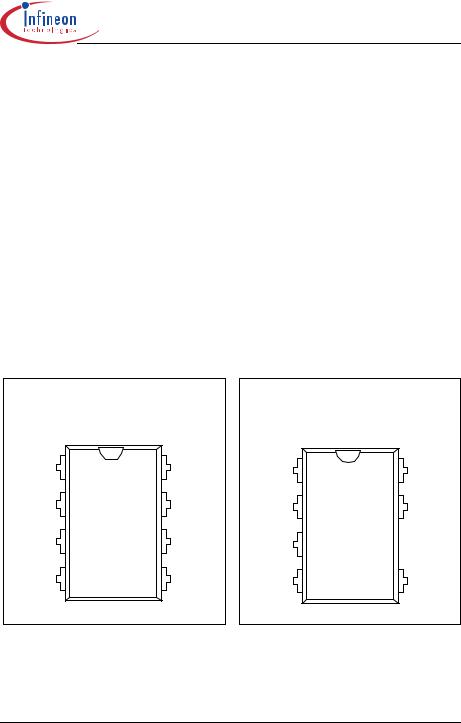
1 Pin Configuration and Functionality
1.1 |
Pin Configuration with P-DIP-8-6 |
1.2 |
Pin Configuration with P-DIP-7-1 |
Pin |
Symbol |
Function |
|
|
|
1 |
SoftS |
Soft-Start |
|
|
|
2 |
FB |
Feedback |
|
|
|
3 |
Isense |
Controller Current Sense Input, |
|
|
CoolMOS™ Source Output |
4 |
Drain |
650V1)/800V2) CoolMOS™ Drain |
5 |
Drain |
650V1)/800V2) CoolMOS™ Drain |
6 |
N.C |
Not connected |
|
|
|
7 |
VCC |
Controller Supply Voltage |
|
|
|
8 |
GND |
Controller Ground |
|
|
|
1)at Tj = 110°C
2)at Tj = 25°C
Pin |
Symbol |
Function |
|
|
|
1 |
SoftS |
Soft-Start |
|
|
|
2 |
FB |
Feedback |
|
|
|
3 |
Isense |
Controller Current Sense Input, |
|
|
CoolMOS™ Source Output |
4 |
N.C. |
Not connected |
|
|
|
5 |
Drain |
650V1)/800V2) CoolMOS™ Drain |
7 |
VCC |
Controller Supply Voltage |
|
|
|
8 |
GND |
Controller Ground |
|
|
|
1)at Tj = 110°C
2)at Tj = 25°C
|
Package P-DIP-8-6 |
|
|
SoftS |
1 |
8 |
GND |
FB |
2 |
7 |
VCC |
Isense |
3 |
6 |
N.C |
|
|
||
Drain |
4 |
5 |
Drain |
|
|
||
|
Package P-DIP-7-1 |
|
|
SoftS |
1 |
8 |
GND |
FB |
2 |
7 |
VCC |
Isense |
3 |
|
|
|
|
|
|
n.c. |
4 |
5 |
Drain |
|
|
||
Figure 1 |
Pin Configuration (top view) |
Figure 2 |
Pin Configuration (top view) |
Datasheet V4.5 |
6 |
Jan 2004 |
CoolSET™-F2
Pin Configuration and Functionality
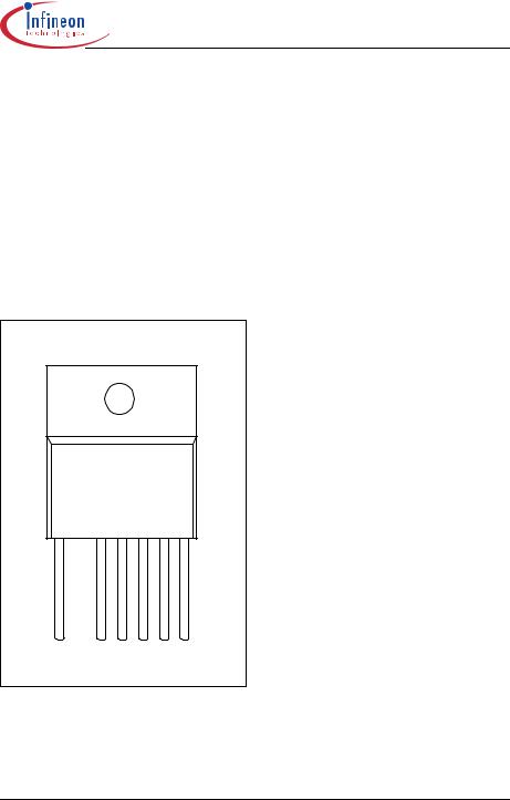
1.3 |
Pin Conuration with P-TO220-6-46/47 1.4 |
Pin Functionality |
Pin |
Symbol |
Function |
|
|
|
|
|
1 |
Drain |
650V1) |
CoolMOS™ Drain |
3 |
Isense |
650V1) |
CoolMOS™ Source |
4 |
GND |
Controller Ground |
|
|
|
|
|
5 |
VCC |
Controller Supply Voltage |
|
|
|
|
|
6 |
SoftS |
Soft-Start |
|
|
|
|
|
7 |
FB |
Feedback |
|
|
|
|
|
1)at Tj = 110°C
Package P-TO220-6-46/47
1 2 3 4 5 6 7
SoftS (Soft Start & Auto Restart Control)
This pin combines the function of Soft Start in case of Start Up and Auto Restart Mode and the controlling of the Auto Restart Mode in case of an error detection.
FB (Feedback)
The information about the regulation is provided by the FB Pin to the internal Protection Unit and to the internal PWM-Comparator to control the duty cycle.
Isense (Current Sense)
The Current Sense pin senses the voltage developed on the series resistor inserted in the source of the integrated CoolMOS™. When Isense reaches the internal threshold of the Current Limit Comparator, the Driver output is disabled. By this means the Over Current Detection is realized.
Furthermore the current information is provided for the PWM-Comparator to realize the Current Mode.
Drain (Drain of integrated CoolMOS™)
Pin Drain is the connection to the Drain of the internal CoolMOSTM.
VCC (Power supply)
This pin is the positiv supply of the IC. The operating range is between 8.5V and 21V.
To provide overvoltage protection the driver gets disabled when the voltage becomes higher than 16.5V during Start Up Phase.
GND (Ground)
This pin is the ground of the primary side of the SMPS.
Drain |
Isense |
GND |
VCC |
SoftS |
FB |
Figure 3 Pin Configuration (top view)
Datasheet V4.5 |
7 |
Jan 2004 |

8 5.V4 Datasheet |
BlockdiagramRepresentative 4 Figure |
FB |
|
|
|
|
|
|
|
|
|
|
|
Current-Limit |
|
|
|
10k |
RSense |
BlockdiagramRepresentative 2 |
|
|
|
|
|
|
|
|
|
|
|
|
|
|
|
|
|
|
|
|
|
|
|
+ |
|
|
|
|
|
|
|
|
|
|
|
|
|
|
|
|
|
|
|
|
|
|
Converter |
|
|
|
|
|
RStart-up |
|
|
CLine |
|
|
|
|
|
|
|
|
|
Snubber |
|
DC Output |
|
||
|
|
85 ... 270 VAC |
|
|
|
|
|
|
|
|
|
|
|
|
|
|
|
|
|
|
VOUT |
|
|
|
|
|
|
|
|
|
|
|
|
|
|
|
|
|
|
|
|
|
|
- |
|
|
|
|
|
|
|
|
|
CVCC |
|
|
|
|
|
|
|
|
|
Drain |
|
|
|
|
|
|
|
|
VCC |
|
|
|
|
|
|
|
|
|
|
|
|
|
|
|
|
|
|
|
|
|
|
|
|
|
|
|
|
|
Power Management |
|
|
|
|
|
|
|
|
|
|
|
|
|
|
|
|
|
|
|
|
Undervoltage |
Internal Bias |
|
|
|
|
|
|
|
|
|
|||
|
|
|
|
|
|
|
|
|
Lockout |
|
|
|
|
|
|
|
|
|
|
|||
|
|
|
|
|
C1 |
|
|
|
|
13.5V |
|
|
|
|
|
|
|
|
|
|
|
|
|
|
|
|
16.5V |
|
|
|
|
8.5V |
|
|
|
|
|
|
Duty Cycle Max |
|
|
|
|
|
|
|
|
|
|
|
|
|
|
|
Power-Down |
|
6.5V |
Oscillator |
|
0.72 |
|
|
|
|
|
|
||
|
|
|
|
|
|
|
|
|
|
Reset |
|
Voltage |
5.3V |
|
|
|
|
|
|
|
|
|
|
|
|
6.5V |
|
|
|
|
|
|
|
|
4.8V |
Duty Cycle |
|
|
|
|
|
|
|
|
|
|
|
|
4.0V |
C2 |
|
|
|
|
|
|
Reference |
4.0V |
max |
|
|
|
|
|
|
|
|
|
|
|
|
|
|
G1 |
|
|
Power-Up |
|
|
|
|
|
|
|
|
|
|
|
|||
|
|
|
RSoft-Start |
|
|
|
|
Reset |
|
|
|
Clock |
|
|
|
|
|
|
|
|
||
|
|
|
|
|
|
|
|
|
|
|
|
fstandby-fnorm |
|
|
|
|
|
|
|
|
||
|
|
SoftS |
|
|
|
|
|
|
|
|
|
Soft Start |
Soft-Start |
|
|
|
|
|
|
|
|
|
|
|
|
|
|
|
|
|
|
|
|
|
|
PWM-Latch |
CoolMOS™ |
|
|
|
|||||
|
|
|
|
|
|
|
|
|
|
|
|
|
Comparator |
|
|
|
|
|
||||
|
|
|
|
|
|
|
|
|
|
|
|
|
|
|
|
S |
Q |
|
|
|
|
|
|
|
|
|
5.6V |
|
|
|
|
|
|
|
|
|
|
|
|
|
|
|
|
|
|
|
|
CSoft-Start |
|
|
C4 |
|
|
Spike |
S |
Q |
|
|
|
|
R |
Q |
|
|
|
|
|
|
|
|
|
|
5.3V |
|
G3 |
Blanking |
|
|
|
|
Gate |
|
|
|
|
||||||
|
|
|
|
|
G2 |
|
|
|
|
|
G4 |
|
|
|
|
|
|
|||||
|
|
T1 |
6.5V |
|
|
|
|
5 s |
|
|
|
|
|
|
|
Driver |
|
|
|
|
||
|
|
|
|
|
|
|
|
|
|
|
|
|
|
|
|
|
|
|
||||
|
|
|
|
4.8V |
C3 |
|
|
|
|
R |
Q |
|
PWM |
|
|
|
|
|
|
|
|
|
|
|
|
RFB |
|
|
|
|
Error-Latch |
|
Comparator |
|
|
|
|
|
|
|
|
|
|||
|
|
|
|
|
|
|
|
|
|
|
|
|
|
|
|
|
|
|
||||
|
|
|
|
|
|
|
|
|
|
|
|
0.3V |
C5 |
|
|
|
|
|
|
|
|
|
|
|
|
|
|
|
|
|
|
|
|
|
|
|
|
|
|
|
|
|
|
|
|
|
|
|
|
Thermal Shutdown |
|
|
|
fosc |
|
|
|
|
Comparator |
|
|
Leading Edge |
|
|
|
|
||
|
|
|
|
|
|
|
|
fnorm |
|
|
|
|
|
|
|
|
Vcsth |
Blanking |
D1 |
Isense |
|
|
|
|
|
|
|
|
|
|
|
|
|
|
|
|
|
|
220ns |
|
|
||||
|
|
|
|
Tj |
>140°C |
|
|
fstandby |
|
UFB |
0.8V |
|
|
|
|
|
|
|
|
BlockdiagramRepresentative |
|
|
2004Jan |
|
|
|
Protection Unit |
|
|
Standby Unit |
|
|
|
|
Propagation-Delay |
|
|
|
|
F2CoolSET™- |
|||||
|
|
|
|
|
|
|
|
x3.65 |
Compensation |
|
|
|
|
|
|
|||||||
|
|
|
|
|
|
|
|
|
|
|
|
|
|
|
|
|
|
|||||
|
|
|
|
|
|
|
|
|
|
|
|
|
|
|
|
|
|
|
|
|
||
|
|
|
|
|
|
|
|
|
|
|
|
PWM OP |
|
|
|
|
|
|
|
|
|
|
|
|
|
|
|
|
|
|
|
|
|
|
Improved Current Mode |
Current Limiting |
|
|
|
|
Optocoupler |
|
|
||
|
|
|
|
|
|
|
|
|
|
|
|
|
|
|
|
|
|
|
|
|
|
|
|
|
|
CoolSET™-F2 |
|
|
|
|
|
|
|
|
|
|
|
|
|
|
|
|
|
|
|
|
|
|
|
|
GND |
|
|
|
|
|
|
|
|
|
|
|
|
|
|
|
|
|
|
|
|
|
|
|
|
|
|
|
|
|
|
|
ICE2Axxxx |
ICE2Bxxxx |
|
|
|
|
|
||
|
|
|
|
|
|
|
|
|
|
|
|
|
fnorm |
100kHz |
|
67kHz |
|
|
|
|
|
|
|
|
|
|
|
|
|
|
|
|
|
|
|
fstandby |
21.5kHz |
|
20kHz |
|
|
|
|
|
|
CoolSET™-F2
Functional Description
3 Functional Description
3.1 |
Power Management |
3.2 |
Improved Current Mode |
|
M ain Line (100V -380V) |
||
|
R S tart-U p |
|
|
|
|
Prim ary W inding |
|
|
C VC C |
||
V C C |
|
|
|
Pow er Managem ent |
|||
U nd ervo ltag e |
|
Intern al |
|
|
|
||
L ockout |
|
B ia s |
|
1 3.5V |
|
||
|
|
||
8 .5V |
|
|
|
P o w er-D ow n |
|
6.5 V |
|
|
|
||
R e set |
|
5.3 V |
|
|
|
V olta ge |
|
|
|
4.8 V |
|
|
|
R e fe rence |
|
P o w e r-U p |
|
4.0 V |
|
|
|
||
R ese t |
|
|
|
|
R |
Q |
|
|
|
P W M -La tch |
|
6.5V |
S |
Q |
|
R S oft-S tart |
|||
E rro r-Latch |
|||
S o ftS |
|||
|
|
||
|
|
S oft-Start Com parator |
|
T 1 |
|
E rror-D e te ctio n |
|
C S oft-Start |
|
|
|
Figure 5 Power Management
The Undervoltage Lockout monitors the external supply voltage VVCC. In case the IC is inactive the current consumption is max. 55µA. When the SMPS is
plugged to the main line the current through RStart-up charges the external Capacitor CVCC. When VVCC
exceeds the on-threshold VCCon=13.5V the internal bias circuit and the voltage reference are switched on. After that the internal bandgap generates a reference voltage VREF=6.5V to supply the internal circuits. To avoid uncontrolled ringing at switch-on a hysteresis is implemented which means that switch-off is only after active mode when Vcc falls below 8.5V.
In case of switch-on a Power Up Reset is done by reseting the internal error-latch in the protection unit.
When VVCC falls below the off-threshold VCCoff=8.5V the internal reference is switched off and the Power Down
reset let T1 discharging the soft-start capacitor CSoft-Start at pin SoftS. Thus it is ensured that at every switch-on
the voltage ramp at pin SoftS starts at zero.
Soft-Start C om parator
FB |
PW M -Latch |
|
|
|
|
|
R |
Q |
|
|
D river |
PW M C om parator |
|
|
|
S |
Q |
0.8V |
|
|
PW M O P |
|
|
x3.65 |
Isense |
|
Im proved |
|
|
Current M ode |
|
|
Figure 6 Current Mode
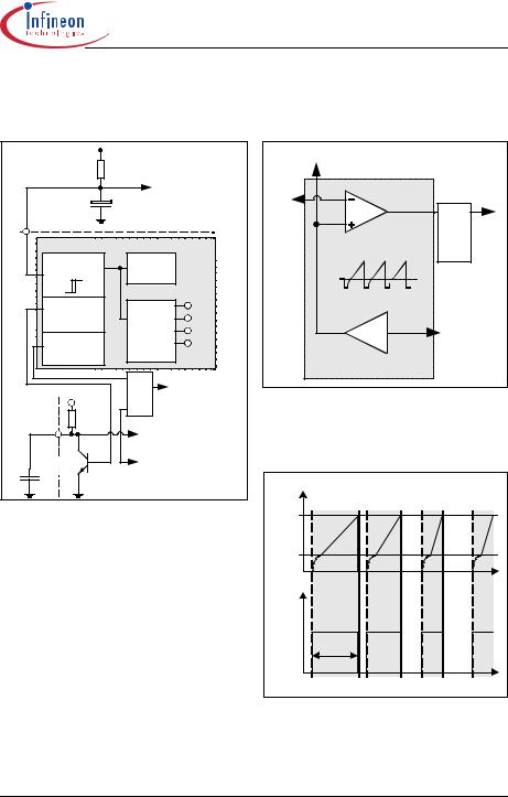
Current Mode means that the duty cycle is controlled by the slope of the primary current. This is done by comparison the FB signal with the amplified current sense signal.
Amplified Current Signal |
|
FB |
|
0.8V |
|
Driver |
t |
Ton |
|
|
t |
Figure 7 Pulse Width Modulation
In case the amplified current sense signal exceeds the FB signal the on-time Ton of the driver is finished by reseting the PWM-Latch (see Figure 7).
Datasheet V4.5 |
9 |
Jan 2004 |
CoolSET™-F2
The primary current is sensed by the external series resistor RSense inserted in the source of the integrated CoolMOS™. By means of Current Mode the regulation of the secondary voltage is insensitive on line variations. Line variation causes varition of the increasing current slope which controls the duty cycle. The external RSense allows an individual adjustment of the maximum source current of the integrated CoolMOS™.
Soft-Start C om parator |
|
|
||
|
|
PW M C om parator |
||
FB |
|
|
|
|
|
|
|
PW M -Latch |
|
O scillator |
0.3V |
|
|
|
|
C 5 |
|
|
|
|
|
G ate D river |
||
V O S C |
|
|
||
|
|
0.8V |
|
|
|
|
10kΩ |
|
x3.65 |
|
|
R 1 |
|
|
T |
2 |
V 1 |
|
|
|
|
PW M O P |
||
|
C 1 |
20pF |
||
|
|
|
||
Voltage Ram p |
|
|
|
|
Figure 8 Improved Current Mode
To improve the Current Mode during light load conditions the amplified current ramp of the PWM-OP is superimposed on a voltage ramp, which is built by the switch T2, the voltage source V1 and the 1st order low pass filter composed of R1 and C1(see Figure 8, Figure 9). Every time the oscillator shuts down for max. duty cycle limitation the switch T2 is closed by VOSC. When the oscillator triggers the Gate Driver T2 is opened so that the voltage ramp can start.
In case of light load the amplified current ramp is to small to ensure a stable regulation. In that case the Voltage Ramp is a well defined signal for the comparison with the FB-signal. The duty cycle is then controlled by the slope of the Voltage Ramp.
By means of the Comparator C5, the Gate Driver is switched-off until the voltage ramp exceeds 0.3V. It allows the duty cycle to be reduced continously till 0% by decreasing VFB below that threshold.
Functional Description
VOSC |
|
max. |
|
Duty Cycle |
|
Voltage Ramp |
t |
|
|
0.8V |
|
FB |
|
0.3V |
|
Gate Driver |
t |
|
|
|
t |
Figure 9 Light Load Conditions
3.2.1PWM-OP
The input of the PWM-OP is applied over the internal leading edge blanking to the external sense resistor
RSense connected to pin ISense. RSense converts the source current into a sense voltage. The sense voltage
is amplified with a gain of 3.65 by PWM OP. The output of the PWM-OP is connected to the voltage source V1. The voltage ramp with the superimposed amplified current singal is fed into the positive inputs of the PWMComparator, C5 and the Soft-Start-Comparator.
3.2.2PWM-Comparator
The PWM-Comparator compares the sensed current signal of the integrated CoolMOSTM with the feedback signal VFB (see Figure 10). VFB is created by an external optocoupler or external transistor in combination with the internal pullup resistor RFB and provides the load information of the feedback circuitry. When the amplified current signal of the integrated CoolMOS™ exceeds the signal V FB the PWMComparator switches off the Gate Driver.
Datasheet V4.5 |
10 |
Jan 2004 |
CoolSET™-F2
|
6.5V |
R FB |
Soft-Start C om parator |
FB |
PW M -Latch |
|
|
|
PW M C om parator |
|
0.8V |
O ptocoupler |
PW M O P |
|
|
|
Isense |
|
x3.65 |
|
Im proved |
|
Current M ode |
Figure 10 PWM Controlling
3.3Soft-Start
V S oftS |
|
5.6V |
|
5.3V |
|
T S oft-S tart |
|
G ate D river |
t |
|
t |
Functional Description
pullup resistor RSoft-Start. The Soft-Start-Comparator compares the voltage at pin SoftS at the negative input
with the ramp signal of the PWM-OP at the positive
input. When Soft-Start voltage VSoftS is less than Feedback voltage VFB the Soft-Start-Comparator limits
the pulse width by reseting the PWM-Latch (see Figure 11). In addition to Start-Up, Soft-Start is also activated at each restart attempt during Auto Restart. By means
of the above mentioned CSoft-Start the Soft-Start can be defined by the user. The Soft-Start is finished when
VSoftS exceeds 5.3V. At that time the Protection Unit is activated by Comparator C4 and senses the FB by
Comparator C3 wether the voltage is below 4.8V which means that the voltage on the secondary side of the SMPS is settled. The internal Zener Diode at SoftS with breaktrough voltage of 5.6V is to prevent the internal circuit from saturation (see Figure 12).
|
|
|
|
|
|
|
|
|
|
|
|
6 .5 V |
|
|
|
|
|
|
|
||||||||||
|
5 .6V |
|
|
|
|
|
|
|
|
|
|
P ow er-U p R eset |
|||||||||||||||||
|
|
|
|
|
|
|
|
|
R S oft-S tart |
|
|
|
|
E rror-Latch |
|||||||||||||||
|
|
|
|
|
|
|
|
|
|
|
|
|
|
|
|
|
|
|
|
||||||||||
|
|
|
|
|
|
|
|
|
|
|
|
|
|
|
|
|
|||||||||||||
|
|
|
|
|
|
|
|
|
|
|
|
|
|
|
|
||||||||||||||
|
S oftS |
|
|
|
|
|
|
|
|
|
C 4 |
|
|
|
|
|
|
|
R |
Q |
|
|
|||||||
|
6 .5 V |
|
|
|
|
|
|
|
G 2 |
|
|
|
S |
Q |
|
|
|||||||||||||
|
|
|
|
|
|
|
5 .3V |
|
|
|
|
|
|
|
|
|
|
|
|
|
|
||||||||
|
|
|
|
|
|
|
4 .8V |
|
|
|
|
|
|
|
|
|
|
|
|
|
|
|
|
|
|
||||
|
|
|
|
|
|
|
|
|
|
|
|
|
|
|
|
|
|
|
|
|
|
|
|
|
|||||
|
|
|
|
R F B |
|
|
|
|
|
C 3 |
|
|
|
|
|
|
|
R |
Q |
|
|
||||||||
|
|
|
|
|
|
|
|
|
|
|
|
|
|
|
|
G ate |
|||||||||||||
|
|
|
|
|
|
|
|
|
|
|
|
|
|
|
|
|
|
|
|
|
|
|
|
|
|
|
|
||
|
F B |
|
|
|
|
|
|
C lock |
|
|
|
S |
Q |
D river |
|||||||||||||||
|
|
|
|
|
|
|
|
|
|
||||||||||||||||||||
|
|
|
|
|
|
|
|
|
|
|
|
||||||||||||||||||
|
|
|
|
|
|
|
|
|
|
|
|
||||||||||||||||||
P W M -Latch
Figure 12 Activation of Protection Unit
The Start-Up time TStart-Up within the converter output voltage VOUT is settled must be shorter than the Soft-
Start Phase TSoft-Start (see Figure 13).
CSoft – Start |
TSoft – Start |
= ------------------------------------- |
|
|
RSoft – Start × 1.69 |
By means of Soft-Start there is an effective minimization of current and voltage stresses on the integrated CoolMOS™, the clamp circuit and the output overshoot and prevents saturation of the transformer during Start-Up.
Figure 11 Soft-Start Phase
The Soft-Start is realized by the internal pullup resistor
RSoft-Start and the external Capacitor CSoft-Start (see Figure 2). The Soft-Start voltage VSoftS is generated by charging the external capacitor CSoft-Start by the internal
Datasheet V4.5 |
11 |
Jan 2004 |
Loading...