


INFINEON HYS72D32300GBR–5–C, HYS72D64300GBR–5–C, HYS72D64320GBR–5–C, HYS72D32300GBR–6–C, HYS72D64300GBR–6–C User Manual
...
HYS72D128320GBR-6-C |
Data Sheet, Rev. 1.0, Mar. 2004 |
|
|
|
|
HYS72D32300GBR–[5/6]–C
HYS72D64300GBR–[5/6]–C
HYS72D64320GBR–[5/6]–C
HYS72D128320GBR–6–C
184-Pin Registered Double Data Rate SDRAM Module
Reg DIMM
DDR SDRAM
Memory Products
N e v e r s t o p t h i n k i n g .
Edition 2004-03
Published by Infineon Technologies AG, St.-Martin-Strasse 53,
81669 München, Germany
© Infineon Technologies AG 2004. All Rights Reserved.
Attention please!
The information herein is given to describe certain components and shall not be considered as a guarantee of characteristics.
Terms of delivery and rights to technical change reserved.
We hereby disclaim any and all warranties, including but not limited to warranties of non-infringement, regarding circuits, descriptions and charts stated herein.
Information
For further information on technology, delivery terms and conditions and prices please contact your nearest Infineon Technologies Office (www.infineon.com).
Warnings
Due to technical requirements components may contain dangerous substances. For information on the types in question please contact your nearest Infineon Technologies Office.
Infineon Technologies Components may only be used in life-support devices or systems with the express written approval of Infineon Technologies, if a failure of such components can reasonably be expected to cause the failure of that life-support device or system, or to affect the safety or effectiveness of that device or system. Life support devices or systems are intended to be implanted in the human body, or to support and/or maintain and sustain and/or protect human life. If they fail, it is reasonable to assume that the health of the user or other persons may be endangered.

Data Sheet, Rev. 1.0, Mar. 2004
HYS72D32300GBR–[5/6]–C HYS72D64300GBR–[5/6]–C HYS72D64320GBR–[5/6]–C HYS72D128320GBR–6–C
184-Pin Registered Double Data Rate SDRAM Module
Reg DIMM
DDR SDRAM
Memory Products
N e v e r s t o p t h i n k i n g .

HYS72D32300GBR–[5/6]–C HYS72D64300GBR–[5/6]–C HYS72D64320GBR–[5/6]–C HYS72D128320GBR– 6–CHYS72D64300GBR–[5/6]–C HYS72D64320GBR–[5/6]–C
Revision History: |
Rev. 1.0 |
2004-03 |
|
Previous Version: |
Rev. 0.5 |
|
|
|
|
|
|
Page |
Subjects (major changes since last revision) |
|
|
|
|
|
|
20,21 |
Idd values updated |
|
|
8,22 |
editorial changes |
|
|
|
|
|
|
24,27 |
Changed SPD Code Byte 99 - 127 to FF |
|
|
|
|
|
|
We Listen to Your Comments
Any information within this document that you feel is wrong, unclear or missing at all? Your feedback will help us to continuously improve the quality of this document. Please send your proposal (including a reference to this document) to:
techdoc.mp@infineon.com
Template: mp_a4_v2.2_2003-10-07.fm

HYS72D[128/64/32][300/320]GBR–[5/6]–C
Registered Double Data Rate SDRAM
Table of Contents
1 |
Overview . . . . . . . . . . . . . . . . . . . . . . . . . . . . . . . . . . . . . . . . . . . . . . . . . . . . . . . . . . . . . . . . . . . . . . |
. 6 |
1.1 |
Features . . . . . . . . . . . . . . . . . . . . . . . . . . . . . . . . . . . . . . . . . . . . . . . . . . . . . . . . . . . . . . . . . . . . . . . . |
6 |
1.2 |
Description . . . . . . . . . . . . . . . . . . . . . . . . . . . . . . . . . . . . . . . . . . . . . . . . . . . . . . . . . . . . . . . . . . . . . . |
6 |
2 |
Pin Configuration . . . . . . . . . . . . . . . . . . . . . . . . . . . . . . . . . . . . . . . . . . . . . . . . . . . . . . . . . . . . . . . . |
8 |
3 |
Electrical Characteristics . . . . . . . . . . . . . . . . . . . . . . . . . . . . . . . . . . . . . . . . . . . . . . . . . . . . . . . . . |
17 |
3.1 |
Operating Conditions . . . . . . . . . . . . . . . . . . . . . . . . . . . . . . . . . . . . . . . . . . . . . . . . . . . . . . . . . . . . . |
17 |
4 |
Current Specification and Conditions . . . . . . . . . . . . . . . . . . . . . . . . . . . . . . . . . . . . . . . . . . . . . . |
19 |
4.1 |
AC Characteristics . . . . . . . . . . . . . . . . . . . . . . . . . . . . . . . . . . . . . . . . . . . . . . . . . . . . . . . . . . . . . . . |
22 |
5 |
SPD Contents . . . . . . . . . . . . . . . . . . . . . . . . . . . . . . . . . . . . . . . . . . . . . . . . . . . . . . . . . . . . . . . . . . |
24 |
6 |
Package Outlines . . . . . . . . . . . . . . . . . . . . . . . . . . . . . . . . . . . . . . . . . . . . . . . . . . . . . . . . . . . . . . . |
30 |
7 |
Application Note . . . . . . . . . . . . . . . . . . . . . . . . . . . . . . . . . . . . . . . . . . . . . . . . . . . . . . . . . . . . . . . . |
34 |
Data Sheet |
5 |
Rev. 1.0, 2004-03 |

HYS72D[128/64/32][300/320]GBR–[5/6]–C
Registered Double Data Rate SDRAM
Overview
1 Overview
1.1Features
•184-Pin Registered 8-Byte Dual-In-Line
DDR SDRAM Module for “1U” PC, Workstation and Server main memory applications
•One rank 32 M × 72 and 64M × 72 and two ranks 64 M ×72 and 128 M ×72 organization
•JEDEC standard Double Data Rate Synchronous DRAMs (DDR SDRAM) with a single + 2.5 V (± 0.2 V) power supply and + 2.6 V (± 0.1 V) power supply for DDR400
•Built with 256-Mbit DDR SDRAMs in P-TFBGA-60-1 packages
•Programmable CAS Latency, Burst Length, and Wrap Sequence (Sequential & Interleave)
•Auto Refresh (CBR) and Self Refresh
•All inputs and outputs SSTL_2 compatible
•Re-drive for all input signals using register and PLL devices.
•Serial Presence Detect with E2PROM
•Low Profile Modules form factor:
133.35 mm × 28.58 mm × 4.00 mm / 2.64 mm and for 1GB 133.35 mm × 30.48 mm (1.2”)× 4.00 mm
•JEDEC standard reference layout for one rank 256 MB, 512 MB and two ranks 512 MB, 1 GB: PC2700 and PC3200 Registered DIMM Raw Cards A,B,C,D
•Gold plated contacts
Table 1 |
Performance |
|
|
|
|
|
|
|
|
|
|
|
|
Part Number Speed Code |
|
|
–5 |
–6 |
Unit |
|
|
|
|
|
|
|
|
Speed Grade |
Component |
|
DDR400B |
DDR333B |
— |
|
|
|
|
|
|
|
|
|
|
Module |
|
PC3200–3033 |
PC2700–2533 |
— |
|
|
|
|
|
|
|
max. Clock Frequency |
@CL3 |
fCK3 |
200 |
166 |
MHz |
|
|
|
@CL2.5 |
fCK2.5 |
166 |
166 |
MHz |
|
|
@CL2 |
fCK2 |
133 |
133 |
MHz |
1.2Description
The HYS72D[128/64/32][300/320]GBR–[5/6]–C and HYS72D64320GBR–5–C are low profile versions of the standard Registered DIMM modules suitable for 1U Server Applications. The Low Profile DIMM versions are available as 32 M ×72 (256 MB), 64 M ×72 (512 MB) and 128 M ×72 (1 GB)
The memory array is designed with Double Data Rate Synchronous DRAMs for ECC applications. All control and address signals are re-driven on the DIMM using register devices and a PLL for the clock distribution. This reduces capacitive loading to the system bus, but adds one cycle to the SDRAM timing. A variety of decoupling capacitors are mounted on the PC board. The DIMMs feature serial presence detect based on a serial E2PROM device using the 2-pin I2C protocol. The first 128 bytes are programmed with configuration data and the second 128 bytes are available to the customer.
Data Sheet |
6 |
Rev. 1.0, 2004-03 |
|
|
07302003-2MI6-FOP1 |

HYS72D[128/64/32][300/320]GBR–[5/6]–C
Registered Double Data Rate SDRAM
Overview
Table 2 |
Ordering Information |
|
|
|
Type |
|
Compliance Code |
Description |
SDRAM |
|
|
|
|
Technology |
|
|
|
|
|
PC3200 (CL = 3.0) |
|
|
|
|
|
|
|
|
|
HYS72D32300GBR–5–C |
PC3200R–30330–A0 |
1 Rank 256 MB Registered DIMM ECC |
256 Mbit (×8) |
|
|
|
|
|
|
HYS72D64300GBR–5–C |
PC3200R–30330–C0 |
1 Rank 512 MB Registered DIMM ECC |
256 Mbit (×4) |
|
|
|
|
|
|
HYS72D64320GBR–5–C |
PC3200R–30330–B0 |
2 Ranks 512 MB Registered DIMM ECC |
256 Mbit (×8) |
|
|
|
|
|
|
PC2700 (CL = 2.5, tRP = tRCD = 3 at tCK = 6ns)
HYS72D32300GBR–6–C |
PC2700R–25330–A0 |
1 Rank 256 MB Registered DIMM ECC |
256 Mbit (×8) |
|
|
|
|
HYS72D64300GBR–6–C |
PC2700R–25330–C0 |
1 Rank 512 MB Registered DIMM ECC |
256 Mbit (×4) |
|
|
|
|
HYS72D64320GBR–6–C |
PC2700R–25330–B0 |
2 Ranks 512 MB Registered DIMM ECC |
256 Mbit (×8) |
|
|
|
|
HYS72D128320GBR–6–C |
PC2700R–25330–D0 |
2 Ranks 1 GB Registered DIMM ECC |
256 Mbit (×4) |
|
|
|
|
Data Sheet |
7 |
Rev. 1.0, 2004-03 |
|
|
07302003-2MI6-FOP1 |

HYS72D[128/64/32][300/320]GBR–[5/6]–C
Registered Double Data Rate SDRAM
Pin Configuration
2 Pin Configuration
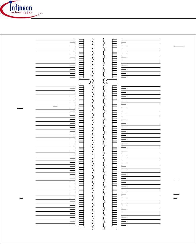
The pin configuration of the Registered DDR SDRAM DIMM is listed by function in Table 3 (184 pins). The abbreviations used in columns Pin and Buffer Type are explained in Table 4 and Table 5 respectively. The pin numbering is depicted in Figure 1.
Table 3 Pin Configuration of RDIMM
Pin# Name Pin Buffer Function
Type Type
Clock Signals
137 |
|
|
CK0 |
|
I |
SSTL |
Clock Signal |
|||||
|
|
|
|
|
|
|
|
|
|
|
|
|
138 |
|
|
|
|
|
|
|
|
I |
SSTL |
Complement Clock |
|
CK0 |
||||||||||||
|
|
|
|
|
|
|||||||
21 |
CKE0 |
|
I |
SSTL |
Clock Enable Rank 0 |
|||||||
|
|
|
|
|
|
|
|
|||||
111 |
|
|
CKE1 |
|
I |
SSTL |
Clock Enable Rank 1 |
|||||
|
|
|
|
|
|
|
|
|
|
|
Note: 2-rank module |
|
|
|
|
|
|
|
|
|
|||||
|
|
|
NC |
|
NC |
SSTL |
Note: 1-rank module |
|||||
|
|
|
|
|
|
|||||||
Control Signals |
|
|
|
|||||||||
|
|
|
|
|
|
|
|
|
|
|
||
157 |
|
|
S0 |
|
|
|
|
I |
SSTL |
Chip Select of Rank 0 |
||
|
|
|
|
|
|
|
|
|
|
|
||
158 |
|
|
|
|
|
|
|
I |
SSTL |
Chip Select of Rank 1 |
||
|
|
S1 |
||||||||||
|
|
|
|
|
|
|
|
|
|
|
Note: 2-ranks module |
|
|
|
|
|
|
|
|
|
|||||
|
|
|
NC |
|
NC |
– |
Note: 1-rank module |
|||||
|
|
|
|
|
|
|
|
|
|
|||
154 |
|
|
|
|
|
|
|
|
I |
SSTL |
Row Address Strobe |
|
RAS |
||||||||||||
|
|
|
|
|
|
|
|
|
||||
65 |
|
|
|
|
|
|
|
|
I |
SSTL |
Column Address |
|
|
CAS |
|||||||||||
|
|
|
|
|
|
|
|
|
|
|
Strobe |
|
|
|
|
|
|
|
|
|
|
||||
63 |
|
|
|
|
|
|
I |
SSTL |
Write Enable |
|||
|
WE |
|||||||||||
|
|
|
|
|
|
|
||||||
10 |
|
|
|
|
|
|
|
|
I |
LV- |
Register Reset |
|
RESET |
||||||||||||
|
|
|
|
|
|
|
|
|
|
CMOS |
Forces registered |
|
|
|
|
|
|
|
|
|
|
|
|
inputs low |
|
|
|
|
|
|
|
|
|
|
|
|
Note: For |
detailed |
|
|
|
|
|
|
|
|
|
|
|
description of the |
|
|
|
|
|
|
|
|
|
|
|
|
Power |
Up and |
|
|
|
|
|
|
|
|
|
|
|
Power |
|
|
|
|
|
|
|
|
|
|
|
|
Management see |
|
|
|
|
|
|
|
|
|
|
|
|
the |
Application |
|
|
|
|
|
|
|
|
|
|
|
Note at the end of |
|
|
|
|
|
|
|
|
|
|
|
|
data sheet |
|
|
|
|
|
|
|
|||||||
Address Signals |
|
|
|
|||||||||
|
|
|
|
|
|
|||||||
59 |
BA0 |
|
I |
SSTL |
Bank Address Bus |
|||||||
|
|
|
|
|
|
|
|
|
|
|
1:0 |
|
52 |
BA1 |
|
I |
SSTL |
|
|||||||
|
|
|
||||||||||
|
|
|
|
|
|
|||||||
48 |
A0 |
|
I |
SSTL |
Address Bus 11:0 |
|||||||
|
|
|
|
|
|
|
||||||
43 |
A1 |
|
I |
SSTL |
|
|
||||||
|
|
|
|
|
|
|
||||||
41 |
A2 |
|
I |
SSTL |
|
|
||||||
|
|
|
|
|
|
|
|
|
||||
130 |
|
|
A3 |
|
I |
SSTL |
|
|
||||
|
|
|
|
|
|
|
||||||
37 |
A4 |
|
I |
SSTL |
|
|
||||||
|
|
|
|
|
|
|||||||
32 |
A5 |
|
I |
SSTL |
Address Bus 11:0 |
|||||||
|
|
|
|
|
|
|
|
|
|
|
|
|
Table 3 |
Pin Configuration of RDIMM (cont’d) |
|||||
Pin# |
Name |
|
Pin |
Buffer |
Function |
|
|
|
|
Type |
Type |
|
|
|
|
|
|
|
|
|
125 |
A6 |
|
I |
SSTL |
Address Bus 11:0 |
|
|
|
|
|
|
|
|
29 |
A7 |
|
I |
SSTL |
|
|
|
|
|
|
|
|
|
122 |
A8 |
|
I |
SSTL |
|
|
|
|
|
|
|
|
|
27 |
A9 |
|
I |
SSTL |
|
|
|
|
|
|
|
|
|
141 |
A10 |
|
I |
SSTL |
|
|
|
|
|
|
|
|
|
|
AP |
|
I |
SSTL |
|
|
|
|
|
|
|
|
|
118 |
A11 |
|
I |
SSTL |
|
|
|
|
|
|
|
|
|
115 |
A12 |
|
I |
SSTL |
Address Signal 12 |
|
|
|
|
|
|
Note: Module based on |
|
|
|
|
|
|
256 Mbit or larger |
|
|
|
|
|
|
dies |
|
|
|
|
|
|
|
|
|
NC |
|
NC |
– |
Note: 128 Mbit |
based |
|
|
|
|
|
module |
|
|
|
|
|
|
|
|
167 |
A13 |
|
I |
SSTL |
Address Signal 13 |
|
|
|
|
|
|
Note: 1 Gbit |
based |
|
|
|
|
|
module |
|
|
|
|
|
|
|
|
|
NC |
|
NC |
– |
Note: Module based on |
|
|
|
|
|
|
512 Mbit |
or |
|
|
|
|
|
smaller dies |
|
|
|
|
|
|
|
|
Data Sheet |
8 |
Rev. 1.0, 2004-03 |

HYS72D[128/64/32][300/320]GBR–[5/6]–C
Registered Double Data Rate SDRAM
Table 3 Pin Configuration of RDIMM (cont’d)
Pin# Name Pin Buffer Function
Type Type
Data Signals
2 |
DQ0 |
I/O |
SSTL |
Data Bus 63:0 |
|
|
|
|
|
4 |
DQ1 |
I/O |
SSTL |
|
|
|
|
|
|
6 |
DQ2 |
I/O |
SSTL |
|
|
|
|
|
|
8 |
DQ3 |
I/O |
SSTL |
|
|
|
|
|
|
94 |
DQ4 |
I/O |
SSTL |
|
|
|
|
|
|
95 |
DQ5 |
I/O |
SSTL |
|
|
|
|
|
|
98 |
DQ6 |
I/O |
SSTL |
|
|
|
|
|
|
99 |
DQ7 |
I/O |
SSTL |
|
|
|
|
|
|
12 |
DQ8 |
I/O |
SSTL |
|
|
|
|
|
|
13 |
DQ9 |
I/O |
SSTL |
|
|
|
|
|
|
19 |
DQ10 |
I/O |
SSTL |
|
|
|
|
|
|
20 |
DQ11 |
I/O |
SSTL |
|
|
|
|
|
|
105 |
DQ12 |
I/O |
SSTL |
|
|
|
|
|
|
106 |
DQ13 |
I/O |
SSTL |
|
|
|
|
|
|
109 |
DQ14 |
I/O |
SSTL |
|
|
|
|
|
|
110 |
DQ15 |
I/O |
SSTL |
|
|
|
|
|
|
23 |
DQ16 |
I/O |
SSTL |
|
|
|
|
|
|
24 |
DQ17 |
I/O |
SSTL |
|
|
|
|
|
|
28 |
DQ18 |
I/O |
SSTL |
|
|
|
|
|
|
31 |
DQ19 |
I/O |
SSTL |
|
|
|
|
|
|
114 |
DQ20 |
I/O |
SSTL |
|
|
|
|
|
|
117 |
DQ21 |
I/O |
SSTL |
|
|
|
|
|
|
121 |
DQ22 |
I/O |
SSTL |
|
|
|
|
|
|
123 |
DQ23 |
I/O |
SSTL |
|
|
|
|
|
|
33 |
DQ24 |
I/O |
SSTL |
|
|
|
|
|
|
35 |
DQ25 |
I/O |
SSTL |
|
|
|
|
|
|
39 |
DQ26 |
I/O |
SSTL |
|
|
|
|
|
|
40 |
DQ27 |
I/O |
SSTL |
|
|
|
|
|
|
126 |
DQ28 |
I/O |
SSTL |
|
|
|
|
|
|
127 |
DQ29 |
I/O |
SSTL |
|
|
|
|
|
|
131 |
DQ30 |
I/O |
SSTL |
|
|
|
|
|
|
133 |
DQ31 |
I/O |
SSTL |
|
|
|
|
|
|
53 |
DQ32 |
I/O |
SSTL |
|
|
|
|
|
|
55 |
DQ33 |
I/O |
SSTL |
|
|
|
|
|
|
57 |
DQ34 |
I/O |
SSTL |
|
|
|
|
|
|
60 |
DQ35 |
I/O |
SSTL |
|
|
|
|
|
|
146 |
DQ36 |
I/O |
SSTL |
|
|
|
|
|
|
147 |
DQ37 |
I/O |
SSTL |
|
|
|
|
|
|
Pin Configuration
Table 3 Pin Configuration of RDIMM (cont’d)
Pin# |
Name |
Pin |
Buffer |
Function |
|
|
|
|
Type |
Type |
|
|
|
|
|
|
|
|
|
|
150 |
DQ38 |
I/O |
SSTL |
Data Bus 63:0 |
|
|
|
|
|
|
|
|
|
151 |
DQ39 |
I/O |
SSTL |
|
|
|
|
|
|
|
|
|
|
61 |
DQ40 |
I/O |
SSTL |
|
|
|
|
|
|
|
|
|
|
64 |
DQ41 |
I/O |
SSTL |
|
|
|
|
|
|
|
|
|
|
68 |
DQ42 |
I/O |
SSTL |
|
|
|
|
|
|
|
|
|
|
69 |
DQ43 |
I/O |
SSTL |
|
|
|
|
|
|
|
|
|
|
153 |
DQ44 |
I/O |
SSTL |
|
|
|
|
|
|
|
|
|
|
155 |
DQ45 |
I/O |
SSTL |
|
|
|
|
|
|
|
|
|
|
161 |
DQ46 |
I/O |
SSTL |
|
|
|
|
|
|
|
|
|
|
162 |
DQ47 |
I/O |
SSTL |
|
|
|
|
|
|
|
|
|
|
72 |
DQ48 |
I/O |
SSTL |
|
|
|
|
|
|
|
|
|
|
73 |
DQ49 |
I/O |
SSTL |
|
|
|
|
|
|
|
|
|
|
79 |
DQ50 |
I/O |
SSTL |
|
|
|
|
|
|
|
|
|
|
80 |
DQ51 |
I/O |
SSTL |
|
|
|
|
|
|
|
|
|
|
165 |
DQ52 |
I/O |
SSTL |
|
|
|
|
|
|
|
|
|
|
166 |
DQ53 |
I/O |
SSTL |
|
|
|
|
|
|
|
|
|
|
170 |
DQ54 |
I/O |
SSTL |
|
|
|
|
|
|
|
|
|
|
171 |
DQ55 |
I/O |
SSTL |
|
|
|
|
|
|
|
|
|
|
83 |
DQ56 |
I/O |
SSTL |
|
|
|
|
|
|
|
|
|
|
84 |
DQ57 |
I/O |
SSTL |
|
|
|
|
|
|
|
|
|
|
87 |
DQ58 |
I/O |
SSTL |
|
|
|
|
|
|
|
|
|
|
88 |
DQ59 |
I/O |
SSTL |
|
|
|
|
|
|
|
|
|
|
174 |
DQ60 |
I/O |
SSTL |
|
|
|
|
|
|
|
|
|
|
175 |
DQ61 |
I/O |
SSTL |
|
|
|
|
|
|
|
|
|
|
178 |
DQ62 |
I/O |
SSTL |
|
|
|
|
|
|
|
|
|
|
179 |
DQ63 |
I/O |
SSTL |
|
|
|
|
|
|
|
|
|
|
44 |
CB0 |
I/O |
SSTL |
Check Bits 7:0 |
|
|
|
|
|
|
|
|
|
45 |
CB1 |
I/O |
SSTL |
|
|
|
|
|
|
|
|
|
|
49 |
CB2 |
I/O |
SSTL |
|
|
|
|
|
|
|
|
|
|
51 |
CB3 |
I/O |
SSTL |
|
|
|
|
|
|
|
|
|
|
134 |
CB4 |
I/O |
SSTL |
|
|
|
|
|
|
|
|
|
|
135 |
CB5 |
I/O |
SSTL |
|
|
|
|
|
|
|
|
|
|
142 |
CB6 |
I/O |
SSTL |
|
|
|
|
|
|
|
|
|
|
144 |
CB7 |
I/O |
SSTL |
|
|
|
|
|
|
|
|
|
|
5 |
DQS0 |
I/O |
SSTL |
Data Strobes 8:0 |
|
|
|
|
|
|
Note: See |
block |
|
14 |
DQS1 |
I/O |
SSTL |
|||
|
|
|
|
diagram |
for |
|
25 |
DQS2 |
I/O |
SSTL |
|||
corresponding |
||||||
|
|
|
|
|||
36 |
DQS3 |
I/O |
SSTL |
|||
DQ signals |
|
|||||
|
|
|
|
|
||
56 |
DQS4 |
I/O |
SSTL |
|
|
|
|
|
|
|
|
|
|
67 |
DQS5 |
I/O |
SSTL |
|
|
|
|
|
|
|
|
|
|
Data Sheet |
9 |
Rev. 1.0, 2004-03 |

HYS72D[128/64/32][300/320]GBR–[5/6]–C
Registered Double Data Rate SDRAM
Table 3 |
Pin Configuration of RDIMM (cont’d) |
||||
Pin# |
Name |
|
Pin |
Buffer |
Function |
|
|
|
Type |
Type |
|
|
|
|
|
|
|
78 |
DQS6 |
|
I/O |
SSTL |
Data Strobes 8:0 |
|
|
|
|
|
|
86 |
DQS7 |
|
I/O |
SSTL |
|
|
|
|
|
|
|
47 |
DQS8 |
|
I/O |
SSTL |
|
|
|
|
|
|
|
97 |
DM0 |
|
I |
SSTL |
Data Mask 0 |
|
|
|
|
|
Note: ×8 based module |
|
|
|
|
|
|
|
DQS9 |
|
I/O |
SSTL |
Data Strobe 9 |
|
|
|
|
|
Note: ×4 based module |
|
|
|
|
|
|
107 |
DM1 |
|
I |
SSTL |
Data Mask 1 |
|
|
|
|
|
Note: ×8 based module |
|
|
|
|
|
|
|
DQS10 |
I/O |
SSTL |
Data Strobe 10 |
|
|
|
|
|
|
Note: ×4 based module |
|
|
|
|
|
|
119 |
DM2 |
|
I |
SSTL |
Data Mask 2 |
|
|
|
|
|
Note: ×8 based module |
|
|
|
|
|
|
|
DQS11 |
I/O |
SSTL |
Data Strobe 11 |
|
|
|
|
|
|
Note: ×4 based module |
|
|
|
|
|
|
129 |
DM3 |
|
I |
SSTL |
Data Mask 3 |
|
|
|
|
|
Note: ×8 based module |
|
|
|
|
|
|
|
DQS12 |
I/O |
SSTL |
Data Strobe 12 |
|
|
|
|
|
|
Note: ×4 based module |
|
|
|
|
|
|
149 |
DM4 |
|
I |
SSTL |
Data Mask 4 |
|
|
|
|
|
Note: ×8 based module |
|
|
|
|
|
|
|
DQS13 |
I/O |
SSTL |
Data Strobe 13 |
|
|
|
|
|
|
Note: ×4 based module |
|
|
|
|
|
|
159 |
DM5 |
|
I |
SSTL |
Data Mask 5 |
|
|
|
|
|
Note: ×8 based module |
|
|
|
|
|
|
|
DQS14 |
I/O |
SSTL |
Data Strobe 14 |
|
|
|
|
|
|
Note: ×4 based module |
|
|
|
|
|
|
169 |
DM6 |
|
I |
SSTL |
Data Mask 6 |
|
|
|
|
|
Note: ×8 based module |
|
|
|
|
|
|
|
DQS15 |
I/O |
SSTL |
Data Strobe 15 |
|
|
|
|
|
|
Note: ×4 based module |
|
|
|
|
|
|
177 |
DM7 |
|
I |
SSTL |
Data Mask 7 |
|
|
|
|
|
Note: ×8 based module |
|
|
|
|
|
|
|
DQS16 |
I/O |
SSTL |
Data Strobe 16 |
|
|
|
|
|
|
Note: ×4 based module |
|
|
|
|
|
|
140 |
DM8 |
|
I |
SSTL |
Data Mask 8 |
|
|
|
|
|
Note: ×8 based module |
|
|
|
|
|
|
|
DQS17 |
I/O |
SSTL |
Data Strobe 17 |
|
|
|
|
|
|
Note: ×4 based module |
|
|
|
|
|
|
Pin Configuration
Table 3 Pin Configuration of RDIMM (cont’d)
Pin# Name Pin Buffer Function
Type Type
EEPROM
92 |
SCL |
I |
CMOS |
Serial Bus Clock |
|
|
|
|
|
91 |
SDA |
I/O |
OD |
Serial Bus Data |
|
|
|
|
|
181 |
SA0 |
I |
CMOS |
Slave Address Select |
|
|
|
|
Bus 2:0 |
182 |
SA1 |
I |
CMOS |
|
|
|
|
|
|
183 |
SA2 |
I |
CMOS |
|
|
|
|
|
|
Power Supplies |
|
|
||
|
|
|
|
|
1 |
VREF |
AI |
– |
I/O Reference Voltage |
184 |
VDDSPD |
PWR |
– |
EEPROM Power |
|
|
|
|
Supply |
|
|
|
|
|
15, |
VDDQ |
PWR |
– |
I/O Driver Power |
22, |
|
|
|
Supply |
30, |
|
|
|
|
54, |
|
|
|
|
62, |
|
|
|
|
77, |
|
|
|
|
96, |
|
|
|
|
104, |
|
|
|
|
112, |
|
|
|
|
128, |
|
|
|
|
136, |
|
|
|
|
143, |
|
|
|
|
156, |
|
|
|
|
164, |
|
|
|
|
172, |
|
|
|
|
180 |
|
|
|
|
|
|
|
|
|
7, |
VDD |
PWR |
– |
Power Supply |
38, |
|
|
|
|
46, |
|
|
|
|
70, |
|
|
|
|
85, |
|
|
|
|
108, |
|
|
|
|
120, |
|
|
|
|
148, |
|
|
|
|
168 |
|
|
|
|
|
|
|
|
|
Data Sheet |
10 |
Rev. 1.0, 2004-03 |
HYS72D[128/64/32][300/320]GBR–[5/6]–C
Registered Double Data Rate SDRAM
Table 3 Pin Configuration of RDIMM (cont’d)
Pin# |
Name |
Pin |
Buffer |
Function |
|
|
Type |
Type |
|
|
|
|
|
|
3, |
VSS |
GND |
– |
Ground Plane |
11, |
|
|
|
|
18, |
|
|
|
|
26, |
|
|
|
|
34, |
|
|
|
|
42, |
|
|
|
|
50, |
|
|
|
|
58, |
|
|
|
|
66, |
|
|
|
|
74, |
|
|
|
|
81, |
|
|
|
|
89, |
|
|
|
|
93, |
|
|
|
|
100, |
|
|
|
|
116, |
|
|
|
|
124, |
|
|
|
|
132, |
|
|
|
|
139, |
|
|
|
|
145, |
|
|
|
|
152, |
|
|
|
|
160, |
|
|
|
|
176 |
|
|
|
|
|
|
|
|
|
Other Pins
|
|
Pin Configuration |
Table 4 |
Abbreviations for Pin Type |
|
|
|
|
Abbreviation |
|
Description |
|
|
|
I |
|
Standard input-only pin. Digital levels. |
|
|
|
O |
|
Output. Digital levels. |
|
|
|
I/O |
|
I/O is a bidirectional input/output signal. |
|
|
|
AI |
|
Input. Analog levels. |
|
|
|
PWR |
|
Power |
|
|
|
GND |
|
Ground |
|
|
|
NU |
|
Not Usable (JEDEC Standard) |
|
|
|
NC |
|
Not Connected (JEDEC Standard) |
|
|
|
Table 5 |
Abbreviations for Buffer Type |
|
|
|
|
Abbreviation |
|
Description |
|
|
|
SSTL |
|
Serial Stub Terminalted Logic (SSTL2) |
|
|
|
LV-CMOS |
|
Low Voltage CMOS |
|
|
|
CMOS |
|
CMOS Levels |
|
|
|
OD |
|
Open Drain. The corresponding pin has 2 |
|
|
operational states, active low and tristate, |
|
|
and allows multiple devices to share as a |
|
|
wire-OR. |
|
|
|
82 |
VDDID |
O |
OD |
VDD Identification |
|
|
|
|
|
|
Note: Pin |
in tristate, |
|
|
|
|
|
indicating |
VDD |
|
|
|
|
|
and |
VDDQ |
nets |
|
|
|
|
connected |
on |
|
|
|
|
|
PCB |
|
|
|
|
|
|
|
|
|
9, |
NC |
NC |
– |
Not connected |
|
|
16, |
|
|
|
Pins not connected on |
||
17, |
|
|
|
Infineon RDIMM’s |
|
|
71, |
|
|
|
|
|
|
75, |
|
|
|
|
|
|
76, |
|
|
|
|
|
|
90, |
|
|
|
|
|
|
101, |
|
|
|
|
|
|
102, |
|
|
|
|
|
|
103, |
|
|
|
|
|
|
113, |
|
|
|
|
|
|
163, |
|
|
|
|
|
|
173 |
|
|
|
|
|
|
|
|
|
|
|
|
|
Data Sheet |
11 |
Rev. 1.0, 2004-03 |
HYS72D[128/64/32][300/320]GBR–[5/6]–C
Registered Double Data Rate SDRAM
Pin Configuration
VREF - Pin 001
DQS0 - Pin 005
NC - Pin 009
DQ09 - Pin 013
NC - Pin 017
CKE0 - Pin 021
DQS2 - Pin 025
A7 - Pin 029
DQ24 - Pin 033
A4 - Pin 037
A2 - Pin 041
CB01 - Pin 045
CB02 - Pin 049
DQ32 - Pin 053
DQ34 - Pin 057
DQ40 - Pin 061
CAS - Pin 065
DQ43 - Pin 069
DQ49 - Pin 073
VDDQ - Pin 077
VSS - Pin 081
VDD - Pin 085
VSS - Pin 089
VSS - Pin 093
DM00/DQS9 - Pin 097
NC - Pin 101
DQ12 - Pin 105
DQ14 - Pin 109
NC - Pin 113
DQ21 - Pin 117
DQ22 - Pin 121
A6 - Pin 125
DM3/DQS12 - Pin 129
DQ31 - Pin 133
CK0 - Pin 137
A10/AP - Pin 141
VSS - Pin 145
DM4/DQS13 - Pin 149
DQ44 - Pin 153
S0 - Pin 157
DQ46 - Pin 161
DQ52 - Pin 165
DM6/DQS15 - Pin 169
NC - Pin 173
DM7/DQS16 - Pin 177
SA0 - Pin 181
VSS - Pin 003
VDD - Pin 007
VSS - Pin 011
VDDQ - Pin 015
DQ10 - Pin 019
DQ16 - Pin 023
A9 - Pin 027
DQ19 - Pin 031
DQ25 - Pin 035
DQ26 - Pin 039
A1 - Pin 043
DQS8 - Pin 047
CB03 - Pin 051
DQ33 - Pin 055
BA0 - Pin 059
WE - Pin 063
DQS5 - Pin 067
NC - Pin 071
NC - Pin 075
DQ50 - Pin 079
DQ56 - Pin 083
DQ58 - Pin 087
SDA - Pin 091
DQ05 - Pin 095
DQ07 - Pin 099
NC - Pin 103
DM1/DQS10 - Pin 107
CKE1/NC - Pin 111
A12/NC - Pin 115
DM2/DQS11 - Pin 119
DQ23 - Pin 123
DQ29 - Pin 127
DQ30 - Pin 131
CB5 - Pin 135
VSS - Pin 139
VDDQ - Pin 143
DQ37 - Pin 147
DQ39 - Pin 151
DQ45 - Pin 155
DM5/DQS14 - Pin 159
NC - Pin 163
A13/NC - Pin 167
DQ55 - Pin 171
DQ61 - Pin 175
DQ63 - Pin 179
SA2 - Pin 183
FRONTSIDE |
BACKSIDE |
Pin 004 - DQ01
Pin 008 - DQ03
Pin 012 - DQ08
Pin 016 - NC
Pin 020 - DQ11
Pin 024 - DQ17
Pin 028 - DQ18
Pin 032 - A5
Pin 036 - DQS3
Pin 040 - DQ27
Pin 044 - CB00
Pin 048 - A0
Pin 052 - BA1
Pin 056 - DQS4
Pin 060 - DQ35
Pin 064 - DQ41
Pin 068 - DQ42
Pin 072 - DQ48
Pin 076 - NC
Pin 080 - DQ51
Pin 084 - DQ57
Pin 088 - DQ59
Pin 092 - SCL
Pin 096 - VDDQ
Pin 100 - VSS
Pin 104 - VDDQ
Pin 108 - VDD
Pin 112 - VDDQ
Pin 116 - VSS
Pin 120 - VDD
Pin 124 - VSS
Pin 128 - VDDQ
Pin 132 - VSS
Pin 136 - VDDQ
Pin 140 - DM8/DQS17
Pin 144 - CB07
Pin 148 - VDD
Pin 152 - VSS
Pin 156 - VDDQ
Pin 160 - VSS
Pin 164 - VDDQ
Pin 168 - VDD
Pin 172 - VDDQ
Pin 176 - VSS
Pin 180 - VDDQ
Pin 184 - VDDSPD
Pin 002 - DQ00
Pin 006 - DQ02
Pin 010 - RESET
Pin 014 - DQS1
Pin 018 - VSS
Pin 022 - VDDQ
Pin 026 - VSS
Pin 030 - VDDQ
Pin 034 - VSS
Pin 038 - VDD
Pin 042 - VSS
Pin 046 - VDD
Pin 050 - VSS
Pin 054 - VDDQ
Pin 058 - VSS
Pin 062 - VDDQ
Pin 066 - VSS
Pin 070 - VDD
Pin 074 - VSS
Pin 078 - DQS6
Pin 082 - VDDID
Pin 086 - DQS7
Pin 090 - NC
Pin 094 - DQ04
Pin 098 - DQ06
Pin 102 - NC
Pin 106 - DQ13
Pin 110 - DQ15
Pin 114 - DQ20
Pin 118 - A11
Pin 122 - A8
Pin 126 - DQ28
Pin 130 - A3
Pin 134 - DQ04
Pin 138 - CK0
Pin 142 - CB06
Pin 146 - DQ36
Pin 150 - DQ38
Pin 154 - RAS
Pin 158 - S1 /NC
Pin 162 - DQ47
Pin 166 - DQ53
Pin 170 - DQ54
Pin 174 - DQ60
Pin 178 - DQ62
Pin 182 - SA1
MPPD0020
Figure 1 Pin Configuration 184 Pins, Reg |
|
|
|
|
|
|
|
|||
Table 6 |
Address Table |
|
|
|
|
|
|
|
|
|
|
|
|
|
|
|
|
|
|
||
Density |
Organization |
Memory |
SDRAMs |
# of SDRAMs |
# of row/rank/ |
Refresh |
Period |
Interval |
||
|
|
Ranks |
|
|
columns bits |
|
|
|
||
|
|
|
|
|
|
|
|
|
|
|
256 MB |
32 M ×72 |
1 |
32 M ×8 |
9 |
13 |
/ 2 |
/ 10 |
8 K |
64 ms |
7.8 µs |
|
|
|
|
|
|
|
|
|
|
|
512 MB |
64 M ×72 |
1 |
64 M ×4 |
18 |
13 |
/ 2 |
/ 11 |
8 K |
64 ms |
7.8 µs |
|
|
|
|
|
|
|
|
|
|
|
Data Sheet |
|
|
12 |
|
|
|
|
Rev. 1.0, 2004-03 |
||
 Loading...