


 Loading...
INFINEON HYS64T32000GU–5–A, HYS64T64000GU–5–A, HYS72T64000GU–5–A, HYS64T128020GU–5–A, HYS72T128020GU–5–A DATA SHEET
...
Data Sheet, Rev. 0.87, June 2004
HYS64T32000[G/H]U–[3.7/5]–A
HYS[64/72]T64000[G/H]U–[3.7/5]–A
HYS[64/72]T128020[G/H]U–[3.7/5]–A
240-Pin Unbuffered DDR2 SDRAM Modules
DDR2 SDRAM
Memory Products
N e v e r s t o p t h i n k i n g .
The information in this document is subject to change without notice.
Edition 2004-06
Published by Infineon Technologies AG, St.-Martin-Strasse 53,
81669 München, Germany
© Infineon Technologies AG 2004. All Rights Reserved.
Attention please!
The information herein is given to describe certain components and shall not be considered as a guarantee of characteristics.
Terms of delivery and rights to technical change reserved.
We hereby disclaim any and all warranties, including but not limited to warranties of non-infringement, regarding circuits, descriptions and charts stated herein.
Information
For further information on technology, delivery terms and conditions and prices please contact your nearest Infineon Technologies Office (www.infineon.com).
Warnings
Due to technical requirements components may contain dangerous substances. For information on the types in question please contact your nearest Infineon Technologies Office.
Infineon Technologies Components may only be used in life-support devices or systems with the express written approval of Infineon Technologies, if a failure of such components can reasonably be expected to cause the failure of that life-support device or system, or to affect the safety or effectiveness of that device or system. Life support devices or systems are intended to be implanted in the human body, or to support and/or maintain and sustain and/or protect human life. If they fail, it is reasonable to assume that the health of the user or other persons may be endangered.

Data Sheet, Rev. 0.87, June 2004
HYS64T32000[G/H]U–[3.7/5]–A
HYS[64/72]T64000[G/H]U–[3.7/5]–A
HYS[64/72]T128020[G/H]U–[3.7/5]–A
240-Pin Unbuffered DDR2 SDRAM Modules
DDR2 SDRAM
Memory Products
N e v e r s t o p t h i n k i n g .

HYS[64T[3200/6400/12802]0/72T[6400/12802]0][G/H]U–[3.7/5]–A |
|
||
Revision History: |
Rev. 0.87 |
2004-06 |
|
|
|
|
|
Previous Revision: |
Rev. 0.84 |
2003-09 |
|
|
|
|
|
Page |
Subjects (major changes since last revision) |
|
|
|
|
|
|
all |
New template |
|
|
|
|
|
|
chapter 5 |
add currents |
|
|
|
|
|
|
all |
updated timings |
|
|
|
|
|
|
We Listen to Your Comments
Any information within this document that you feel is wrong, unclear or missing at all? Your feedback will help us to continuously improve the quality of this document. Please send your proposal (including a reference to this document) to:
techdoc.mp@infineon.com
Template: mp_a4_v2.3_2004-01-14.fm

HYS[64T[3200/6400/12802]0/72T[6400/12802]0][G/H]U–[3.7/5]–A
512 Mbit DDR2 SDRAM
Table of Contents
1 |
Overview . . . . . . . . . . . . . . . . . . . . . . . . . . . . . . . . . . . . . . . . . . . . . . . . . . . . . . . . . . . . . . . . . . . . . . |
. 6 |
1.1 |
Features . . . . . . . . . . . . . . . . . . . . . . . . . . . . . . . . . . . . . . . . . . . . . . . . . . . . . . . . . . . . . . . . . . . . . . . . |
6 |
1.2 |
Description . . . . . . . . . . . . . . . . . . . . . . . . . . . . . . . . . . . . . . . . . . . . . . . . . . . . . . . . . . . . . . . . . . . . . . |
6 |
1.3 |
Pin Configuration . . . . . . . . . . . . . . . . . . . . . . . . . . . . . . . . . . . . . . . . . . . . . . . . . . . . . . . . . . . . . . . . . |
9 |
2 |
Block Diagrams . . . . . . . . . . . . . . . . . . . . . . . . . . . . . . . . . . . . . . . . . . . . . . . . . . . . . . . . . . . . . . . . . |
18 |
3 |
Electrical Characteristics . . . . . . . . . . . . . . . . . . . . . . . . . . . . . . . . . . . . . . . . . . . . . . . . . . . . . . . . . |
23 |
3.1 |
Operating Conditions . . . . . . . . . . . . . . . . . . . . . . . . . . . . . . . . . . . . . . . . . . . . . . . . . . . . . . . . . . . . . |
23 |
4 |
IDD Specifications and Conditions . . . . . . . . . . . . . . . . . . . . . . . . . . . . . . . . . . . . . . . . . . . . . . . . . |
24 |
4.1 |
IDD Test Conditions . . . . . . . . . . . . . . . . . . . . . . . . . . . . . . . . . . . . . . . . . . . . . . . . . . . . . . . . . . . . . . . |
27 |
4.2 |
ODT (On Die Termination) Current . . . . . . . . . . . . . . . . . . . . . . . . . . . . . . . . . . . . . . . . . . . . . . . . . . . |
27 |
5 |
Electrical Characteristics & AC Timings . . . . . . . . . . . . . . . . . . . . . . . . . . . . . . . . . . . . . . . . . . . . |
28 |
5.1 |
AC Timing Parameter by Speed Grade (Component level data, for reference only) . . . . . . . . . . . . . |
28 |
6 |
SPD Codes . . . . . . . . . . . . . . . . . . . . . . . . . . . . . . . . . . . . . . . . . . . . . . . . . . . . . . . . . . . . . . . . . . . . |
31 |
7 |
Package Outlines . . . . . . . . . . . . . . . . . . . . . . . . . . . . . . . . . . . . . . . . . . . . . . . . . . . . . . . . . . . . . . . |
62 |
7.1 |
Raw Card A . . . . . . . . . . . . . . . . . . . . . . . . . . . . . . . . . . . . . . . . . . . . . . . . . . . . . . . . . . . . . . . . . . . . |
62 |
7.2 |
Raw Card B . . . . . . . . . . . . . . . . . . . . . . . . . . . . . . . . . . . . . . . . . . . . . . . . . . . . . . . . . . . . . . . . . . . . |
63 |
7.3 |
Raw Card C . . . . . . . . . . . . . . . . . . . . . . . . . . . . . . . . . . . . . . . . . . . . . . . . . . . . . . . . . . . . . . . . . . . . |
64 |
8 |
Product Type Nomenclature (DDR2 DRAMs and DIMMs) . . . . . . . . . . . . . . . . . . . . . . . . . . . . . . . |
65 |
Data Sheet |
5 |
Rev. 0.87, 2004-06 |
|
|
09122003-GZEK-H4J6 |

HYS[64T[3200/6400/12802]0/72T[6400/12802]0][G/H]U–[3.7/5]–A
512 Mbit DDR2 SDRAM
Overview
1 Overview
This chapter gives an overview of the 1.8 V 240-pin Unbuffered DDR2 SDRAM Modules, 256 MByte, 512 MByte & 1 GByte ECC and non-ECC Modules and describes its main characteristics.
1.1Features
•240-pin ECC and Non-ECC Unbuffered 8-Byte Dual-In-Line DDR2 SDRAM Module for PC, Workstation and Server main memory applications
•One rank 32M x 64, 64M x 64, 64M x 72 and two ranks 128M × 64 and 128M x 72 organization
•JEDEC standard Double Data Rate 2 Synchronous
DRAMs (DDR2 SDRAM) with a single + 1.8 V (± 0.1 V) power supply
•256 ,512 MByte and 1GByte modules built with
512Mb DDR2 SDRAMs in 60-ball (P–TFBGA–60) and 84-ball FBGA (P–TFBGA–84) chipsize packages
•Programmable CAS Latencies (3, 4 & 5), Burst Length (8 & 4) and Burst Type
•Auto Refresh (CBR) and Self Refresh
•All inputs and outputs SSTL_1.8 compatible
•OCD (Off-Chip Driver Impedance Adjustment) and ODT (On-Die Termination)
•Serial Presence Detect with E2PROM
•Low Profile Modules form factor: 133.35 mm x 30,00 mm (MO-237)
•Based on JEDEC standard reference card layouts Raw Card “A”, “B” & “C”
Table 1 |
Performance |
|
|
|
Speed Grade Indicator |
–5 |
–-3.7 |
Unit |
|
|
|
|
|
|
Component Speed Grade |
DDR2–400 |
DDR2–533 |
— |
|
|
|
|
|
|
Module Speed Grade |
PC2–3200 |
PC2–4200 |
— |
|
|
|
|
|
|
Max. Clock Frequency @ CL = 3 |
200 |
200 |
MHz |
|
|
|
|
|
|
Max. Clock Frequency @ CL = 4 & 5 |
200 |
266 |
MHz |
|
|
|
|
|
|
1.2Description
The INFINEON HYS[64/72]Txxxx0[G/H]U module family are low profile Unbuffered DIMM modules with 30,0 mm height based on DDR2 technology. DIMMs are available as non-ECC modules in 32M x 64 (256MB), 64M x 64 (512MB) and 128M x 64 (1024MB) and as ECC-modules in 64M x 72 (512MB) and 128M x 72 (1024MB) organisation and density, intended for mounting into 240 pin connector sockets.
The memory array is designed with 512Mb Double Data Rate (DDR2) Synchronous DRAMs for ECC and Non-ECC applications. Decoupling capacitors are mounted on the PCB board. The DIMMs feature serial presence detect based on a serial E2PROM device using the 2-pin I2C protocol. The first 128 bytes are programmed with configuration data and the second 128 bytes are available to the customer.
Data Sheet |
6 |
Rev. 0.87, 2004-06 |
|
|
09122003-GZEK-H4J6 |
HYS[64T[3200/6400/12802]0/72T[6400/12802]0][G/H]U–[3.7/5]–A
512 Mbit DDR2 SDRAM
Overview
Table 2 |
Ordering Information |
|
|
|
Product Type |
Compliance Code |
Description |
SDRAM |
|
|
|
|
|
Technology |
|
|
|
|
|
PC2-3200 |
|
|
|
|
|
|
|
|
|
HYS64T32000GU–5–A |
256MB 1R×16 PC2–3200U–333–11–C0 |
1 Rank, Non-ECC |
512 Mbit (×16) |
|
|
|
|
|
|
HYS64T64000GU–5–A |
512MB 1R×8 PC2–3200U–333–11–A0 |
1 Rank, Non-ECC |
512 Mbit (×8) |
|
|
|
|
|
|
HYS72T64000GU–5–A |
512MB 1R×8 PC2–3200E–333–11–A0 |
1 Rank, ECC |
512 Mbit (×8) |
|
|
|
|
|
|
HYS64T128020GU–5–A |
1GB 2R×8 PC2–3200U–333–11–B0 |
2 Ranks, Non-ECC |
512 Mbit (×8 |
|
|
|
|
|
|
HYS72T128020GU–5–A |
1GB 2R×8 PC2–3200E–333–11–B0 |
2 Ranks, ECC |
512 Mbit (×8) |
|
|
|
|
|
|
|
|
|
|
|
HYS64T32000HU–5–A |
256MB 1R×16 PC2–3200U–333–11–C0 |
1 rank, Non-ECC |
512 Mbit (×16) |
|
|
|
|
|
|
HYS64T64000HU–5–A |
512MB 1R×8 PC2–3200U–333–11–A0 |
1 rank, Non-ECC |
512 Mbit (×8) |
|
|
|
|
|
|
HYS72T64000HU–5–A |
512MB 1R×8 PC2–3200E–333–11–A0 |
1 rank, ECC |
512 Mbit (×8) |
|
|
|
|
|
|
HYS64T128020HU–5–A |
1GB 2R×8 PC2–3200U–333–11–B0 |
2 ranks, Non-ECC |
512 Mbit (×8) |
|
|
|
|
|
|
HYS72T128020HU–5–A |
1GB 2R×8 PC2–3200E–333–11–B0 |
2 ranks, ECC |
512 Mbit (×8) |
|
|
|
|
|
|
PC2–4200 |
|
|
|
|
|
|
|
|
|
HYS64T32000GU–3.7–A |
256MB 1R×16 PC2–4200U–444–11–C0 |
1 rank, Non-ECC |
512 Mbit (×16) |
|
|
|
|
|
|
HYS64T64000GU–3.7–A |
512MB 1R×8 PC2–4200U–444–11–A0 |
1 rank, Non-ECC |
512 Mbit (×8) |
|
|
|
|
|
|
HYS72T64000GU–3.7–A |
512MB 1R×8 PC2–4200E–444–11–A0 |
1 rank, ECC |
512 Mbit (×8) |
|
|
|
|
|
|
HYS64T128020GU–3.7–A |
1GB 2R×8 PC2–4200U–444–11–B0 |
2 ranks, Non-ECC |
512 Mbit (×8 |
|
|
|
|
|
|
HYS72T128020GU–3.7–A |
1GB 2R×8 PC2–4200E–444–11–B0 |
2 ranks, ECC |
512 Mbit (×8) |
|
|
|
|
|
|
|
|
|
|
|
HYS64T32000HU–3.7–A |
256MB 1R×16 PC2–4200U–444–11–C0 |
1 rank, Non-ECC |
512 Mbit (×16) |
|
|
|
|
|
|
HYS72T64000HU–3.7–A |
512MB 1R×8 PC2–4200E–444–11–A0 |
1 rank, ECC |
512 Mbit (×8) |
|
|
|
|
|
|
HYS64T64000HU–3.7–A |
512MB 1R×8 PC2–4200U–444–11–A0 |
1 rank, Non-ECC |
512 Mbit (×8) |
|
|
|
|
|
|
HYS64T128020HU–3.7–A |
1GB 2R×8 PC2–4200U–444–11–B0 |
2 ranks, Non-ECC |
512 Mbit (×8) |
|
|
|
|
|
|
HYS72T128020HU–3.7–A |
1GB 2R×8 PC2–4200E–444–11–B0 |
2 ranks, ECC |
512 Mbit (×8) |
|
|
|
|
|
|
Note:
1.All part numbers end with a place code, designating the silicon die revision. Example: HYS72T64000GU–5-A, indicating Rev. A dice are used for DDR2 SDRAM components. For all INFINEON DDR2 module and component nomenclature see section 8 of this datasheet.
2.The Compliance Code is printed on the module label and describes the speed grade, f.e. “PC2-
4200U-44410-C”, where 4200U means Unbuffered DIMM modules with 4.26 GB/sec Module Bandwidth and “44410” means CAS latency = 4, trcd latency = 4 and trp latency = 4 using the latest JEDEC SPD Revision 1.1 and produced on the Raw Card “C”.
Data Sheet |
7 |
Rev. 0.87, 2004-06 |
|
|
09122003-GZEK-H4J6 |

HYS[64T[3200/6400/12802]0/72T[6400/12802]0][G/H]U–[3.7/5]–A
512 Mbit DDR2 SDRAM
Overview
Table 3 |
Address Format |
|
|
|
|
|
|
DIMM |
Module |
|
Memory |
ECC/ |
# of |
# of row/bank/columns bits |
Raw |
Density |
Organization |
|
Ranks |
Non-ECC |
SDRAMs |
|
Card |
|
|
|
|
|
|
|
|
256 MB |
32M ×64 |
|
1 |
Non-ECC |
4 |
13/2/10 |
C |
|
|
|
|
|
|
|
|
512 MB |
64M ×64 |
|
1 |
Non-ECC |
8 |
14/2/10 |
A |
|
|
|
|
|
|
|
|
512 MB |
64M ×72 |
|
1 |
ECC |
9 |
14/2/10 |
A |
|
|
|
|
|
|
|
|
1 GB |
2 × 64M ×72 |
|
2 |
Non-ECC |
16 |
14/2/10 |
B |
|
|
|
|
|
|
|
|
1 GB |
2 × 64M ×72 |
|
2 |
ECC |
18 |
14/2/10 |
B |
|
|
|
|
|
|
|
|
Table 4 |
Components on Modules1) |
|
|
||
Part Number |
DIMM |
DRAM components |
DRAM Density |
DRAM Organisation |
|
|
|
Density |
reference datasheet |
|
|
|
|
|
|
|
|
HYS64T32000GU |
256 MB |
HYB18T512160AC |
512 Mbit |
32M ×16 |
|
|
|
|
|
|
|
HYS64T32000HU2) |
256 MB |
HYB18T512160AF2) |
512 Mbit |
32M ×16 |
|
HYS64T64000GU |
512 MB |
HYB18T512800AC |
512 Mbit |
64Mb ×8 |
|
|
|
|
|
|
|
HYS64T64000HU2) |
512 MB |
HYB18T512800AF2) |
512 Mbit |
64Mb ×8 |
|
HYS72T64000GU |
512 MB |
HYB18T512800AC |
512 Mbit |
64Mb ×8 |
|
|
|
|
|
|
|
HYS72T64000HU2) |
512 MB |
HYB18T512800AF2) |
512 Mbit |
64Mb ×8 |
|
HYS64T128020GU |
1 GB |
HYB18T1G800AC |
512 Mbit |
64Mb ×8 |
|
|
|
|
|
|
|
HYS64T128020HU2) |
1 GB |
HYB18T1G800AF2) |
512 Mbit |
64Mb ×8 |
|
HYS72T128020GU |
1 GB |
HYB18T1G800AC |
512 Mbit |
64Mb ×8 |
|
|
|
|
|
|
|
HYS72T128020HU2) |
1 GB |
HYB18T1G800AF2) |
512 Mbit |
64Mb ×8 |
|
1)For a detailed description of all functionalities of the DRAM components on these modules see the referenced component datasheet.
2)Green Product
Data Sheet |
8 |
Rev. 0.87, 2004-06 |
|
|
09122003-GZEK-H4J6 |

HYS[64T[3200/6400/12802]0/72T[6400/12802]0][G/H]U–[3.7/5]–A
512 Mbit DDR2 SDRAM
Overview
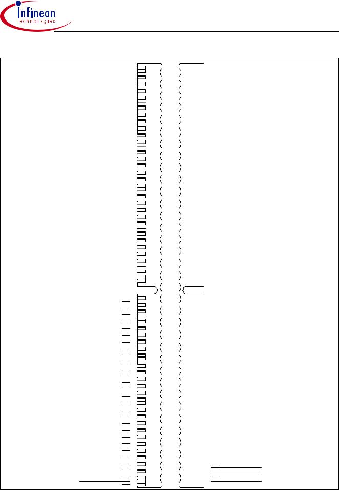
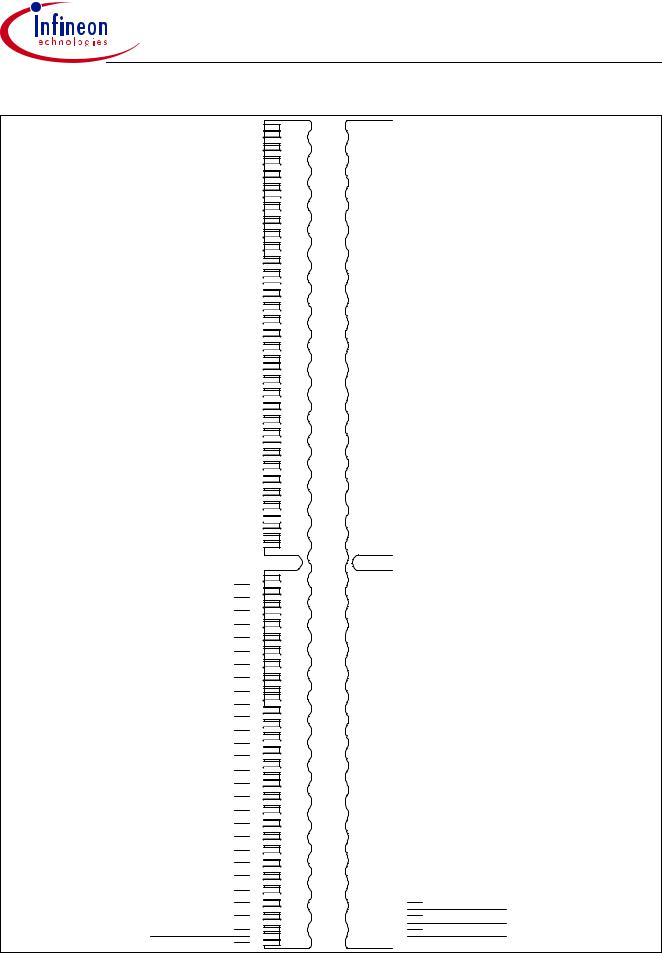
1.3Pin Configuration
The pin configuration of the Unbuffered DDR2 SDRAM DIMM is listed by function in Table 5 (240 pins). The abbreviations used in columns Pin and Buffer Type are explained in Table 6 and Table 7 respectively. The pin numbering is depicted in Figure 1 for non-ECC modules (×64) and Figure 2 for ECC modules (×72).
Table 5 |
Pin Configuration of UDIMM |
|
|
|
|||||||||
Pin# |
|
|
Name |
|
Pin |
Buffer |
Function |
||||||
|
|
|
|
|
|
|
|
|
|
|
Type |
Type |
|
|
|
|
|
|
|
||||||||
Clock Signals |
|
|
|
||||||||||
|
|
|
|
|
|
|
|
|
|||||
185 |
|
|
|
CK0 |
|
I |
SSTL |
Clock Signals 2:0 |
|||||
|
|
|
|
|
|
|
|
|
|||||
137 |
|
|
|
CK1 |
|
I |
SSTL |
|
|||||
|
|
|
|
|
|
|
|
|
|||||
220 |
|
|
|
CK2 |
|
I |
SSTL |
|
|||||
|
|
|
|
|
|
|
|
|
|
|
|
|
|
186 |
|
|
|
|
|
|
|
|
|
|
I |
SSTL |
Complement Clock Signals 2:0 |
CK0 |
|||||||||||||
|
|
|
|
|
|
|
|
|
|
|
|
|
|
138 |
|
|
|
|
|
|
|
|
|
|
I |
SSTL |
|
|
|
CK1 |
|
||||||||||
|
|
|
|
|
|
|
|
|
|
|
|
|
|
221 |
|
|
|
|
|
|
|
|
|
|
I |
SSTL |
|
|
|
CK2 |
|
||||||||||
|
|
|
|
|
|
|
|||||||
52 |
|
CKE0 |
|
I |
SSTL |
Clock Enable Rank 0 |
|||||||
|
|
|
|
|
|
|
|
|
|||||
171 |
|
|
|
CKE1 |
|
I |
SSTL |
Clock Enable Rank 1 |
|||||
|
|
|
|
|
|
|
|
|
|
|
|
|
Note: 2 Ranks module |
|
|
|
|
|
|
|
|
|
|||||
|
|
|
|
NC |
|
NC |
— |
Note: 1 Rank module |
|||||
|
|
|
|
|
|
||||||||
Control Signals |
|
|
|
||||||||||
|
|
|
|
|
|
|
|
|
|
|
|
|
|
193 |
|
|
|
S0 |
|
|
|
|
|
I |
SSTL |
Chip Select Rank 0 |
|
|
|
|
|
|
|
|
|
|
|
|
|
||
76 |
|
|
|
|
|
|
|
|
|
I |
SSTL |
Chip Select Rank 1 |
|
|
|
S1 |
|||||||||||
|
|
|
|
|
|
|
|
|
|
|
|
|
Note: 2 Ranks module |
|
|
|
|
|
|
|
|
|
|||||
|
|
|
|
NC |
|
NC |
— |
Note: 1 Rank module |
|||||
|
|
|
|
|
|
|
|
|
|
|
|||
192 |
|
|
|
|
|
|
|
|
|
|
I |
SSTL |
Row Address Strobe |
|
|
RAS |
|||||||||||
|
|
|
|
|
|
|
|
|
|
||||
74 |
|
|
|
|
|
|
|
|
|
|
I |
SSTL |
Column Address Strobe |
CAS |
|||||||||||||
|
|
|
|
|
|
|
|
|
|||||
73 |
|
|
|
|
|
|
|
|
I |
SSTL |
Write Enable |
||
|
|
WE |
|||||||||||
|
|
|
|
|
|
||||||||
Address Signals |
|
|
|
||||||||||
|
|
|
|
|
|
|
|||||||
71 |
|
BA0 |
|
I |
SSTL |
Bank Address Bus 1:0 |
|||||||
|
|
|
|
|
|
|
|
|
|||||
190 |
|
|
|
BA1 |
|
I |
SSTL |
|
|||||
|
|
|
|
|
|
|
|||||||
54 |
|
BA2 |
|
I |
SSTL |
Bank Address Bus 2 |
|||||||
|
|
|
|
|
|
|
|
|
|
|
|
|
Note: greater than 512Mb DDR2 SDRAMS |
|
|
|
|
|
|
|
|
|
|||||
|
|
|
|
NC |
|
NC |
— |
Note: less than 1Gb DDR2 SDRAMS |
|||||
|
|
|
|
|
|
|
|
|
|||||
188 |
|
|
|
A0 |
|
I |
SSTL |
Address Bus 12:0 |
|||||
|
|
|
|
|
|
|
|
|
|||||
183 |
|
|
|
A1 |
|
I |
SSTL |
|
|||||
|
|
|
|
|
|
|
|||||||
63 |
|
A2 |
|
I |
SSTL |
|
|||||||
|
|
|
|
|
|
|
|
|
|||||
182 |
|
|
|
A3 |
|
I |
SSTL |
|
|||||
|
|
|
|
|
|
|
|||||||
61 |
|
A4 |
|
I |
SSTL |
|
|||||||
|
|
|
|
|
|
|
|||||||
60 |
|
A5 |
|
I |
SSTL |
|
|||||||
|
|
|
|
|
|
|
|
|
|||||
180 |
|
|
|
A6 |
|
I |
SSTL |
|
|||||
|
|
|
|
|
|
|
|||||||
58 |
|
A7 |
|
I |
SSTL |
|
|||||||
|
|
|
|
|
|
|
|
|
|||||
179 |
|
|
|
A8 |
|
I |
SSTL |
|
|||||
|
|
|
|
|
|
|
|
|
|||||
177 |
|
|
|
A9 |
|
I |
SSTL |
|
|||||
|
|
|
|
|
|
|
|
|
|
|
|
|
|
Data Sheet |
9 |
Rev. 0.87, 2004-06 |
|
|
09122003-GZEK-H4J6 |

HYS[64T[3200/6400/12802]0/72T[6400/12802]0][G/H]U–[3.7/5]–A
512 Mbit DDR2 SDRAM
Overview
Table 5 |
Pin Configuration of UDIMM (cont’d) |
|
|||
Pin# |
|
Name |
Pin |
Buffer |
Function |
|
|
|
Type |
Type |
|
|
|
|
|
|
|
70 |
|
A10 |
I |
SSTL |
Address Bus 12:0 |
|
|
|
|
|
|
|
|
AP |
I |
SSTL |
|
|
|
|
|
|
|
57 |
|
A11 |
I |
SSTL |
|
|
|
|
|
|
|
176 |
|
A12 |
I |
SSTL |
|
|
|
|
|
|
|
196 |
|
A13 |
I |
SSTL |
Address Signal 13 |
|
|
|
|
|
Note: 1 Gbit based module and 512M ×4/×8 |
|
|
|
|
|
|
|
|
NC |
NC |
— |
Note: |
|
|
|
|
|
1. Module based on 1 Gbit ×16 |
|
|
|
|
|
2. Module based on 512 Mbit ×16 or smaller |
|
|
|
|
|
|
174 |
|
A14 |
I |
SSTL |
Address Signal 14 |
|
|
|
|
|
Note: Modules based on 2 Gbit |
|
|
|
|
|
|
|
|
NC |
NC |
— |
Note: Modules based on 1 Gbit or smaller |
|
|
|
|
|
|
Data Signals |
|
|
|
||
|
|
|
|
|
|
3 |
|
DQ0 |
I/O |
SSTL |
Data Bus 63:0 |
|
|
|
|
|
|
4 |
|
DQ1 |
I/O |
SSTL |
|
|
|
|
|
|
|
9 |
|
DQ2 |
I/O |
SSTL |
|
|
|
|
|
|
|
10 |
|
DQ3 |
I/O |
SSTL |
|
|
|
|
|
|
|
122 |
|
DQ4 |
I/O |
SSTL |
|
|
|
|
|
|
|
123 |
|
DQ5 |
I/O |
SSTL |
|
|
|
|
|
|
|
128 |
|
DQ6 |
I/O |
SSTL |
|
|
|
|
|
|
|
129 |
|
DQ7 |
I/O |
SSTL |
|
|
|
|
|
|
|
12 |
|
DQ8 |
I/O |
SSTL |
|
|
|
|
|
|
|
13 |
|
DQ9 |
I/O |
SSTL |
|
|
|
|
|
|
|
21 |
|
DQ10 |
I/O |
SSTL |
|
|
|
|
|
|
|
22 |
|
DQ11 |
I/O |
SSTL |
|
|
|
|
|
|
|
131 |
|
DQ12 |
I/O |
SSTL |
|
|
|
|
|
|
|
132 |
|
DQ13 |
I/O |
SSTL |
|
|
|
|
|
|
|
140 |
|
DQ14 |
I/O |
SSTL |
|
|
|
|
|
|
|
141 |
|
DQ15 |
I/O |
SSTL |
|
|
|
|
|
|
|
24 |
|
DQ16 |
I/O |
SSTL |
|
|
|
|
|
|
|
25 |
|
DQ17 |
I/O |
SSTL |
|
|
|
|
|
|
|
30 |
|
DQ18 |
I/O |
SSTL |
|
|
|
|
|
|
|
31 |
|
DQ19 |
I/O |
SSTL |
|
|
|
|
|
|
|
143 |
|
DQ20 |
I/O |
SSTL |
|
|
|
|
|
|
|
144 |
|
DQ21 |
I/O |
SSTL |
|
|
|
|
|
|
|
149 |
|
DQ22 |
I/O |
SSTL |
|
|
|
|
|
|
|
150 |
|
DQ23 |
I/O |
SSTL |
|
|
|
|
|
|
|
33 |
|
DQ24 |
I/O |
SSTL |
|
|
|
|
|
|
|
34 |
|
DQ25 |
I/O |
SSTL |
|
|
|
|
|
|
|
Data Sheet |
10 |
Rev. 0.87, 2004-06 |
|
|
09122003-GZEK-H4J6 |
HYS[64T[3200/6400/12802]0/72T[6400/12802]0][G/H]U–[3.7/5]–A
512 Mbit DDR2 SDRAM
Overview
Table 5 |
Pin Configuration of UDIMM (cont’d) |
|
|||
Pin# |
|
Name |
Pin |
Buffer |
Function |
|
|
|
Type |
Type |
|
|
|
|
|
|
|
39 |
|
DQ26 |
I/O |
SSTL |
Data Bus 63:0 |
|
|
|
|
|
|
40 |
|
DQ27 |
I/O |
SSTL |
|
|
|
|
|
|
|
152 |
|
DQ28 |
I/O |
SSTL |
|
|
|
|
|
|
|
153 |
|
DQ29 |
I/O |
SSTL |
|
|
|
|
|
|
|
158 |
|
DQ30 |
I/O |
SSTL |
|
|
|
|
|
|
|
159 |
|
DQ31 |
I/O |
SSTL |
|
|
|
|
|
|
|
80 |
|
DQ32 |
I/O |
SSTL |
|
|
|
|
|
|
|
81 |
|
DQ33 |
I/O |
SSTL |
|
|
|
|
|
|
|
86 |
|
DQ34 |
I/O |
SSTL |
|
|
|
|
|
|
|
87 |
|
DQ35 |
I/O |
SSTL |
|
|
|
|
|
|
|
199 |
|
DQ36 |
I/O |
SSTL |
|
|
|
|
|
|
|
200 |
|
DQ37 |
I/O |
SSTL |
|
|
|
|
|
|
|
205 |
|
DQ38 |
I/O |
SSTL |
|
|
|
|
|
|
|
206 |
|
DQ39 |
I/O |
SSTL |
|
|
|
|
|
|
|
89 |
|
DQ40 |
I/O |
SSTL |
|
|
|
|
|
|
|
90 |
|
DQ41 |
I/O |
SSTL |
|
|
|
|
|
|
|
95 |
|
DQ42 |
I/O |
SSTL |
|
|
|
|
|
|
|
96 |
|
DQ43 |
I/O |
SSTL |
|
|
|
|
|
|
|
208 |
|
DQ44 |
I/O |
SSTL |
|
|
|
|
|
|
|
209 |
|
DQ45 |
I/O |
SSTL |
|
|
|
|
|
|
|
214 |
|
DQ46 |
I/O |
SSTL |
|
|
|
|
|
|
|
215 |
|
DQ47 |
I/O |
SSTL |
|
|
|
|
|
|
|
98 |
|
DQ48 |
I/O |
SSTL |
|
|
|
|
|
|
|
99 |
|
DQ49 |
I/O |
SSTL |
|
|
|
|
|
|
|
107 |
|
DQ50 |
I/O |
SSTL |
|
|
|
|
|
|
|
108 |
|
DQ51 |
I/O |
SSTL |
|
|
|
|
|
|
|
217 |
|
DQ52 |
I/O |
SSTL |
|
|
|
|
|
|
|
218 |
|
DQ53 |
I/O |
SSTL |
|
|
|
|
|
|
|
226 |
|
DQ54 |
I/O |
SSTL |
|
|
|
|
|
|
|
227 |
|
DQ55 |
I/O |
SSTL |
|
|
|
|
|
|
|
110 |
|
DQ56 |
I/O |
SSTL |
|
|
|
|
|
|
|
111 |
|
DQ57 |
I/O |
SSTL |
|
|
|
|
|
|
|
116 |
|
DQ58 |
I/O |
SSTL |
|
|
|
|
|
|
|
117 |
|
DQ59 |
I/O |
SSTL |
|
|
|
|
|
|
|
229 |
|
DQ60 |
I/O |
SSTL |
|
|
|
|
|
|
|
230 |
|
DQ61 |
I/O |
SSTL |
|
|
|
|
|
|
|
235 |
|
DQ62 |
I/O |
SSTL |
|
|
|
|
|
|
|
236 |
|
DQ63 |
I/O |
SSTL |
|
|
|
|
|
|
|
Data Sheet |
11 |
Rev. 0.87, 2004-06 |
|
|
09122003-GZEK-H4J6 |

HYS[64T[3200/6400/12802]0/72T[6400/12802]0][G/H]U–[3.7/5]–A
512 Mbit DDR2 SDRAM
Overview
Table 5 |
Pin Configuration of UDIMM (cont’d) |
|
|
|
|
|||||||
Pin# |
|
|
|
Name |
|
Pin |
Buffer |
Function |
|
|
|
|
|
|
|
|
|
|
|
Type |
Type |
|
|
|
|
|
|
|
|
|
|
|
|
|
||||
Check Bit Signal |
|
|
|
|
|
|
|
|||||
|
|
|
|
|
|
|
|
|
|
|
|
|
42 |
|
|
|
CB0 |
|
I/O |
SSTL |
Check Bit 0 |
|
|
|
|
|
|
|
|
|
|
|
|
|
Note: ECC type module only |
|
|
|
|
|
|
|
|
|
|
|
|
|
|
|
|
|
|
|
|
NC |
|
NC |
— |
Note: Non-ECC module |
|
|
|
|
|
|
|
|
|
|
|
|
|
|
|
|
|
43 |
|
|
|
CB1 |
|
I/O |
SSTL |
Check Bit 1 |
|
|
|
|
|
|
|
|
|
|
|
|
|
Note: ECC type module only |
|
|
|
|
|
|
|
|
|
|
|
|
|
|
|
|
|
|
|
|
NC |
|
NC |
— |
Note: Non-ECC module |
|
|
|
|
|
|
|
|
|
|
|
|
|
|
|
|
|
48 |
|
|
|
CB2 |
|
I/O |
SSTL |
Check Bit 2 |
|
|
|
|
|
|
|
|
|
|
|
|
|
Note: ECC type module only |
|
|
|
|
|
|
|
|
|
|
|
|
|
|
|
|
|
|
|
|
NC |
|
NC |
— |
Note: Non-ECC module |
|
|
|
|
|
|
|
|
|
|
|
|
|
|
|
|
|
49 |
|
|
|
CB3 |
|
I/O |
SSTL |
Check Bit 3 |
|
|
|
|
|
|
|
|
|
|
|
|
|
Note: ECC type module only |
|
|
|
|
|
|
|
|
|
|
|
|
|
|
|
|
|
|
|
|
NC |
|
NC |
— |
Note: Non-ECC module |
|
|
|
|
|
|
|
|
|
|
|
|
|
|
|
||
161 |
|
|
CB4 |
|
I/O |
SSTL |
Check Bit 4 |
|
|
|
||
|
|
|
|
|
|
|
|
|
Note: ECC type module only |
|
|
|
|
|
|
|
|
|
|
|
|
|
|
|
|
|
|
|
|
NC |
|
NC |
— |
Note: Non-ECC module |
|
|
|
|
|
|
|
|
|
|
|
|
|
|
|
||
162 |
|
|
CB5 |
|
I/O |
SSTL |
Check Bit 5 |
|
|
|
||
|
|
|
|
|
|
|
|
|
Note: ECC type module only |
|
|
|
|
|
|
|
|
|
|
|
|
|
|
|
|
|
|
|
|
NC |
|
NC |
— |
Note: Non-ECC module |
|
|
|
|
|
|
|
|
|
|
|
|
|
|
|
||
167 |
|
|
CB6 |
|
I/O |
SSTL |
Check Bit 6 |
|
|
|
||
|
|
|
|
|
|
|
|
|
Note: ECC type module only |
|
|
|
|
|
|
|
|
|
|
|
|
|
|
|
|
|
|
|
|
NC |
|
NC |
— |
Note: Non-ECC module |
|
|
|
|
|
|
|
|
|
|
|
|
|
|
|
||
168 |
|
|
CB7 |
|
I/O |
SSTL |
Check Bit 7 |
|
|
|
||
|
|
|
|
|
|
|
|
|
Note: ECC type module only |
|
|
|
|
|
|
|
|
|
|
|
|
|
|
|
|
|
|
|
|
NC |
|
NC |
— |
Note: Non-ECC module |
|
|
|
|
|
|
|
|
|
|
|
|
|
||||
Data Strobe Bus |
|
|
|
|
|
|
|
|||||
|
|
|
|
|
|
|
|
|
|
|
|
|
7 |
|
|
|
DQS0 |
|
I/O |
SSTL |
Data Strobe Bus 8:0 |
|
|
|
|
|
|
|
|
|
|
Note: See block diagram |
for |
corresponding |
DQ |
|||
16 |
|
DQS1 |
|
I/O |
SSTL |
|||||||
|
|
|
|
|
|
|
|
|
signals |
|
|
|
28 |
|
DQS2 |
|
I/O |
SSTL |
|
|
|
||||
|
|
|
|
|
|
|||||||
|
|
|
|
|
|
|
|
|
|
|||
37 |
|
DQS3 |
|
I/O |
SSTL |
|
|
|
|
|||
|
|
|
|
|
|
|
|
|
|
|||
84 |
|
DQS4 |
|
I/O |
SSTL |
|
|
|
|
|||
|
|
|
|
|
|
|
|
|
|
|||
93 |
|
DQS5 |
|
I/O |
SSTL |
|
|
|
|
|||
|
|
|
|
|
|
|
|
|
|
|
|
|
105 |
|
|
|
DQS6 |
|
I/O |
SSTL |
|
|
|
|
|
|
|
|
|
|
|
|
|
|
|
|
|
|
114 |
|
|
|
DQS7 |
|
I/O |
SSTL |
|
|
|
|
|
|
|
|
|
|
|
|
|
|
|
|||
45 |
|
DQS8 |
|
I/O |
SSTL |
|
|
|
|
|||
|
|
|
|
|
|
|
|
|
|
|
||
6 |
|
|
|
|
|
|
I/O |
SSTL |
Complement Data Strobe Bus 8:0 |
|
||
|
|
|
DQS0 |
|
||||||||
|
|
|
|
|
|
|
|
Note: See block diagram |
for |
corresponding |
DQ |
|
15 |
|
|
|
|
|
|
I/O |
SSTL |
||||
DQS1 |
||||||||||||
|
|
|
|
|
|
|
|
|
signals |
|
|
|
|
|
|
|
|
|
|
|
|
|
|
|
|
27 |
|
|
DQS2 |
|
I/O |
SSTL |
|
|
|
|||
|
|
|
|
|
|
|
||||||
|
|
|
|
|
|
|
|
|
|
|
||
36 |
|
|
|
|
|
|
I/O |
SSTL |
|
|
|
|
|
|
DQS3 |
|
|
|
|
||||||
|
|
|
|
|
|
|
|
|
|
|
||
83 |
|
|
|
|
|
|
I/O |
SSTL |
|
|
|
|
|
|
DQS4 |
|
|
|
|
||||||
|
|
|
|
|
|
|
|
|
|
|
|
|
Data Sheet |
12 |
Rev. 0.87, 2004-06 |
|
|
09122003-GZEK-H4J6 |

HYS[64T[3200/6400/12802]0/72T[6400/12802]0][G/H]U–[3.7/5]–A
512 Mbit DDR2 SDRAM
Overview
Table 5 |
Pin Configuration of UDIMM (cont’d) |
|
|||||||
Pin# |
|
|
|
Name |
Pin |
Buffer |
Function |
||
|
|
|
|
|
|
|
Type |
Type |
|
|
|
|
|
|
|
|
|
|
|
92 |
|
|
|
|
|
|
I/O |
SSTL |
Complement Data Strobe Bus 8:0 |
|
|
DQS5 |
|||||||
|
|
|
|
|
|
|
|
||
104 |
|
|
|
|
|
|
I/O |
SSTL |
|
|
|
DQS6 |
|
||||||
|
|
|
|
|
|
|
|
||
113 |
|
|
|
|
|
|
I/O |
SSTL |
|
|
|
DQS7 |
|
||||||
|
|
|
|
|
|
|
|
||
46 |
|
|
|
|
|
|
I/O |
SSTL |
|
|
|
DQS8 |
|
||||||
|
|
|
|
|
|
|
|
|
|
Data Mask Signals |
|
|
|
|
|
|
|
||
|
|
|
|
|
|
|
|
||
125 |
|
|
|
DM0 |
I |
SSTL |
Data Mask Bus 8:0 |
||
|
|
|
|
|
|
|
|
||
134 |
|
|
|
DM1 |
I |
SSTL |
|
||
|
|
|
|
|
|
|
|
||
146 |
|
|
|
DM2 |
I |
SSTL |
|
||
|
|
|
|
|
|
|
|
||
155 |
|
|
|
DM3 |
I |
SSTL |
|
||
|
|
|
|
|
|
|
|
||
202 |
|
|
|
DM4 |
I |
SSTL |
|
||
|
|
|
|
|
|
|
|
||
211 |
|
|
|
DM5 |
I |
SSTL |
|
||
|
|
|
|
|
|
|
|
||
223 |
|
|
|
DM6 |
I |
SSTL |
|
||
|
|
|
|
|
|
|
|
||
232 |
|
|
|
DM7 |
I |
SSTL |
|
||
|
|
|
|
|
|
|
|
||
164 |
|
|
|
DM8 |
I |
SSTL |
|
||
|
|
|
|
|
|
|
|
|
|
EEPROM |
|
|
|
|
|
|
|
|
|
|
|
|
|
|
|
|
|||
120 |
|
|
SCL |
I |
CMOS |
Serial Bus Clock |
|||
|
|
|
|
|
|
|
|
||
119 |
|
|
|
SDA |
I/O |
OD |
Serial Bus Data |
||
|
|
|
|
|
|
|
|
||
239 |
|
|
|
SA0 |
I |
CMOS |
Slave Address Select Bus 2:0 |
||
|
|
|
|
|
|
|
|
||
240 |
|
|
|
SA1 |
I |
CMOS |
|
||
|
|
|
|
|
|
|
|
||
101 |
|
|
|
SA2 |
I |
CMOS |
|
||
|
|
|
|
|
|
|
|
|
|
Power Supplies |
|
|
|
|
|
|
|
||
|
|
|
|
|
|
|
|
||
1 |
|
|
|
VREF |
AI |
— |
I/O Reference Voltage |
||
238 |
|
|
|
VDDSPD |
PWR |
— |
EEPROM Power Supply |
||
51,56,62,72,75,78,170,175,181, |
|
|
VDDQ |
PWR |
— |
I/O Driver Power Supply |
|||
191,194 |
|
|
|
|
|
|
|
|
|
|
|
|
|
|
|
|
|||
53,59,64,67,69,172,178,184,187 |
|
|
VDD |
PWR |
— |
Power Supply |
|||
189,197 |
|
|
|
|
|
|
|
|
|
|
|
|
|
|
|
|
|||
2,5,8,11,14,17,20,23,26,29,32, |
|
|
VSS |
GND |
— |
Ground Plane |
|||
35,38,41,44,47,50,65,66,79,82, |
|
|
|
|
|
|
|
|
|
85,88,91,94,97,100,103,106, |
|
|
|
|
|
|
|
|
|
109,112,115,118,121,124,127, |
|
|
|
|
|
|
|
|
|
130,133,136,139,142,145,148, |
|
|
|
|
|
|
|
|
|
151,154,157,160,163,166,169, |
|
|
|
|
|
|
|
|
|
198,201,204,207,210,213,216, |
|
|
|
|
|
|
|
|
|
219,222,225,228,231,234,237 |
|
|
|
|
|
|
|
|
|
|
|
|
|
|
|
|
|
|
|
Other Pins |
|
|
|
|
|
|
|
|
|
|
|
|
|
|
|
|
|
||
195 |
|
|
|
ODT0 |
|
|
On-Die Termination Control 0 |
||
|
|
|
|
|
|
|
|
||
77 |
|
|
|
ODT1 |
|
|
On-Die Termination Control 1 |
||
|
|
|
|
|
|
|
Note: 1 Rank modules |
||
|
|
|
|
NC |
NC |
— |
|||
|
|
|
|
|
|
|
|||
18,19,55,68,102,126,135,147, |
|
|
NC |
NC |
— |
Not connected |
|||
156,165,173,203,212, 224,233 |
|
|
|
|
|
|
|
Note: Pins not connected on Infineon UDIMMs |
|
|
|
|
|
|
|
|
|
|
|
|
|
|
|
|
|
|
|
|
|
Data Sheet |
13 |
Rev. 0.87, 2004-06 |
|
|
09122003-GZEK-H4J6 |

|
|
|
HYS[64T[3200/6400/12802]0/72T[6400/12802]0][G/H]U–[3.7/5]–A |
|
|
|
|
||
|
|
|
|
512 Mbit DDR2 SDRAM |
|
|
|
||
|
|
|
||
|
|
|
|
|
|
|
|
|
Overview |
Table 6 |
Abbreviations for Buffer Type |
|||
|
|
|
||
Abbreviation |
|
Description |
||
|
|
|
|
|
I |
|
|
Standard input-only pin. Digital levels. |
|
|
|
|
|
|
O |
|
|
Output. Digital levels. |
|
|
|
|
|
|
I/O |
|
|
I/O is a bidirectional input/output signal. |
|
|
|
|
|
|
AI |
|
|
Input. Analog levels. |
|
|
|
|
|
|
PWR |
|
|
Power |
|
|
|
|
|
|
GND |
|
|
Ground |
|
|
|
|
|
|
NC |
|
|
Not Connected |
|
|
|
|
||
Table 7 |
Abbreviations for Buffer Type |
|||
|
|
|
||
Abbreviation |
|
Description |
||
|
|
|
|
|
SSTL |
|
|
Serial Stub Terminated Logic (SSTL_18) |
|
|
|
|
|
|
LV-CMOS |
|
|
Low Voltage CMOS |
|
|
|
|
|
|
CMOS |
|
|
CMOS Levels |
|
|
|
|
|
|
OD |
|
|
Open Drain. The corresponding pin has 2 operational states, active low and |
|
|
|
|
|
tristate, and allows multiple devices to share as a wire-OR. |
|
|
|
|
|
Data Sheet |
14 |
Rev. 0.87, 2004-06 |
|
|
09122003-GZEK-H4J6 |
HYS[64T[3200/6400/12802]0/72T[6400/12802]0][G/H]U–[3.7/5]–A
512 Mbit DDR2 SDRAM
Overview
VREF - Pin 001 |
|
|
|
|
|
|
|
|
|||||||
VSS |
- |
Pin 002 |
|
||||||||||||
DQ0 |
- |
Pin 003 |
|
||||||||||||
DQ1 |
- Pin 004 |
|
|||||||||||||
VSS |
- |
Pin 005 |
|
||||||||||||
DQS0 |
- Pin 006 |
|
|||||||||||||
DQS0 - |
Pin 007 |
|
|||||||||||||
VSS |
- |
Pin 008 |
|
||||||||||||
DQ2 |
- |
Pin 009 |
|
||||||||||||
DQ3 |
- Pin 010 |
|
|||||||||||||
VSS |
- |
Pin 011 |
|
||||||||||||
DQ8 |
- Pin 012 |
|
|||||||||||||
DQ9 |
- |
Pin 013 |
|
||||||||||||
VSS |
- |
Pin 014 |
|
||||||||||||
|
|
|
|
|
|
|
|
||||||||
DQS1 - |
Pin 015 |
|
|||||||||||||
DQS1 |
- Pin 016 |
|
|||||||||||||
VSS |
- |
Pin 017 |
|
||||||||||||
NC |
- Pin 018 |
|
|||||||||||||
NC |
- Pin 019 |
|
|||||||||||||
VSS |
- |
Pin 020 |
|
||||||||||||
DQ10 - Pin 021 |
|
||||||||||||||
DQ11 |
- Pin 022 |
|
|||||||||||||
V |
|
|
|
- Pin 023 |
|
||||||||||
SS |
DQ16 |
- Pin 024 |
|
||||||||||||
DQ17 |
- Pin 025 |
|
|||||||||||||
VSS |
- |
Pin 026 |
|
||||||||||||
|
|
|
|
|
|
|
|
||||||||
DQS2 |
- Pin 027 |
|
|||||||||||||
DQS2 |
- Pin 028 |
|
|||||||||||||
VSS |
- Pin 029 |
|
|||||||||||||
DQ18 |
- Pin 030 |
|
|||||||||||||
DQ19 |
- Pin 031 |
|
|||||||||||||
VSS |
- |
Pin 032 |
|||||||||||||
DQ24 |
- Pin 033 |
||||||||||||||
DQ25 |
- Pin 034 |
|
|||||||||||||
VSS |
- Pin 035 |
|
|||||||||||||
DQS3 |
- Pin 036 |
|
|||||||||||||
DQS3 - Pin 037 |
|
||||||||||||||
VSS |
- |
Pin 038 |
|
||||||||||||
DQ26 - Pin 039 |
|
||||||||||||||
DQ27 |
- Pin 040 |
|
|||||||||||||
VSS |
- Pin 041 |
|
|||||||||||||
NC |
- Pin 042 |
|
|||||||||||||
NC |
- Pin 043 |
|
|||||||||||||
VSS |
- |
Pin 044 |
|
||||||||||||
NC |
- Pin 045 |
|
|||||||||||||
NC |
- Pin 046 |
|
|||||||||||||
VSS |
- Pin 047 |
|
|||||||||||||
NC |
- Pin 048 |
|
|||||||||||||
NC |
- Pin 049 |
|
|||||||||||||
VSS |
- |
Pin 050 |
|
||||||||||||
VDDQ |
- Pin 051 |
|
|||||||||||||
CKE0 |
- Pin 052 |
|
|||||||||||||
VDD |
- Pin 053 |
|
|||||||||||||
NC/BA2 |
- Pin 054 |
|
|||||||||||||
NC |
- Pin 055 |
|
|||||||||||||
VDDQ |
- |
Pin 056 |
|
||||||||||||
A11 |
- Pin 057 |
|
|||||||||||||
A7 |
- |
Pin 058 |
|
||||||||||||
VDD |
- Pin 059 |
|
|||||||||||||
A5 |
- |
Pin 060 |
|
||||||||||||
A4 |
- Pin 061 |
|
|||||||||||||
VDDQ |
- |
Pin 062 |
|
||||||||||||
A2 |
- Pin 063 |
|
|||||||||||||
VDD |
- |
Pin 064 |
|
||||||||||||
VSS |
- Pin 065 |
|
|||||||||||||
|
|
|
|
|
|
|
|
||||||||
VSS |
- |
Pin 066 |
|||||||||||||
VDD |
- Pin 067 |
||||||||||||||
NC |
- Pin 068 |
||||||||||||||
VDD |
- Pin 069 |
||||||||||||||
A10/AP |
- |
Pin 070 |
|||||||||||||
BA0 |
- Pin 071 |
|
|
|
|
|
|
|
|
||||||
VDDQ |
- Pin 072 |
||||||||||||||
WE |
|
- Pin 073 |
|||||||||||||
|
|
CAS |
- Pin 074 |
||||||||||||
VDDQ |
- Pin 075 |
||||||||||||||
NC/S1 |
- |
Pin 076 |
|||||||||||||
ODT1 |
- Pin 077 |
||||||||||||||
VDDQ |
- |
Pin 078 |
|||||||||||||
VSS |
- Pin 079 |
||||||||||||||
DQ32 |
- Pin 080 |
||||||||||||||
DQ33 |
- Pin 081 |
||||||||||||||
VSS |
- |
Pin 082 |
|||||||||||||
|
|
|
|
|
|
|
|||||||||
DQS4 |
- Pin 083 |
||||||||||||||
DQS4 |
- Pin 084 |
||||||||||||||
VSS |
- Pin 085 |
||||||||||||||
DQ34 |
- Pin 086 |
||||||||||||||
DQ35 |
- Pin 087 |
||||||||||||||
VSS |
- |
Pin 088 |
|||||||||||||
DQ40 - Pin 089 |
|||||||||||||||
DQ41 |
- Pin 090 |
||||||||||||||
VSS |
- Pin 091 |
||||||||||||||
DQS5 |
- Pin 092 |
||||||||||||||
DQS5 - Pin 093 |
|||||||||||||||
VSS |
- |
Pin 094 |
|||||||||||||
DQ42 - Pin 095 |
|||||||||||||||
DQ43 |
- Pin 096 |
||||||||||||||
VSS |
- Pin 097 |
||||||||||||||
DQ48 |
- Pin 098 |
||||||||||||||
DQ49 |
- Pin 099 |
||||||||||||||
VSS |
- |
Pin 100 |
|||||||||||||
SA2 |
- Pin 101 |
||||||||||||||
NC |
- Pin 102 |
||||||||||||||
VSS |
- Pin 103 |
||||||||||||||
DQS6 |
- Pin 104 |
||||||||||||||
DQS6 |
- Pin 105 |
||||||||||||||
VSS |
- |
Pin 106 |
|||||||||||||
DQ50 |
- Pin 107 |
||||||||||||||
DQ51 |
- Pin 108 |
||||||||||||||
VSS |
- Pin 109 |
||||||||||||||
DQ56 |
- Pin 110 |
||||||||||||||
DQ57 |
- Pin 111 |
||||||||||||||
VSS |
- |
Pin 112 |
|||||||||||||
|
|
|
|
|
|
|
|||||||||
DQS7 |
- Pin 113 |
||||||||||||||
DQS7 |
- Pin 114 |
||||||||||||||
VSS |
- Pin 115 |
||||||||||||||
DQ58 |
- Pin 116 |
||||||||||||||
DQ59 |
- Pin 117 |
||||||||||||||
VSS |
- |
Pin 118 |
|||||||||||||
SDA |
- Pin 119 |
||||||||||||||
SCL |
- Pin 120 |
||||||||||||||
|
|
|
|
|
|
|
|||||||||
FRONTSIDE |
BACKSIDE |
|
|
|
|
|
|
|
|
|
|
|
Pin 122 |
- DQ4 |
|||
|
|
|
|||||
|
|
|
Pin 124 |
- VSS |
|||
|
|
|
|||||
|
|
|
|||||
|
|
|
|||||
|
|
|
Pin 126 |
- NC |
|||
|
|
|
|||||
|
|
|
|||||
|
|
|
|
|
|
|
|
|
|
|
Pin 128 |
- DQ6 |
|||
|
|
|
|||||
|
|
|
|||||
|
|
|
|
|
|
|
|
|
|
|
Pin 130 |
- VSS |
|||
|
|
|
|||||
|
|
|
|||||
|
|
|
|||||
|
|
|
Pin 132 |
- DQ13 |
|||
|
|
|
|||||
|
|
|
|||||
|
|
|
|
|
|
|
|
|
|
|
Pin 134 |
- DM1 |
|||
|
|
|
|||||
|
|
|
|||||
|
|
|
|
|
|
|
|
|
|
|
Pin 136 |
- VSS |
|||
|
|
|
|||||
|
|
|
|||||
|
|
|
|||||
|
|
|
Pin 138 |
- |
CK1 |
|
|
|
|
|
|||||
|
|
|
|
|
|
|
|
|
|
|
Pin 140 |
- DQ14 |
|||
|
|
|
|||||
|
|
|
|||||
|
|
|
|
|
|
|
|
|
|
|
Pin 142 |
- VSS |
|||
|
|
|
|||||
|
|
|
|||||
|
|
|
|||||
|
|
|
Pin 144 |
- DQ21 |
|||
|
|
|
|||||
|
|
|
|||||
|
|
|
|||||
|
|
|
Pin 146 |
- DM2 |
|||
|
|
|
|||||
|
|
|
|||||
|
|
|
|||||
|
|
|
Pin 148 |
- VSS |
|||
|
|
|
|||||
|
|
|
|||||
|
|
|
|||||
|
|
|
Pin 150 |
- DQ23 |
|||
|
|
|
|||||
|
|
|
|||||
|
|
|
|||||
|
|
|
Pin 152 |
- DQ28 |
|||
|
|
|
|||||
|
|
|
|||||
|
|
|
|||||
|
|
|
Pin 154 |
- VSS |
|||
|
|
|
|||||
|
|
|
|||||
|
|
|
|||||
|
|
|
Pin 156 |
- NC |
|||
|
|
|
|||||
|
|
|
|
|
|
|
|
|
|
|
Pin 158 |
- DQ30 |
|||
|
|
|
|||||
|
|
|
|||||
|
|
|
|
|
|
|
|
|
|
|
Pin 160 |
- VSS |
|||
|
|
|
|||||
|
|
|
|||||
|
|
|
|||||
|
|
|
Pin 162 |
- NC |
|||
|
|
|
|||||
|
|
|
|||||
|
|
|
|
|
|
|
|
|
|
|
Pin 164 |
- NC |
|||
|
|
|
|||||
|
|
|
|||||
|
|
|
|
|
|
|
|
|
|
|
Pin 166 |
- VSS |
|||
|
|
|
|||||
|
|
|
|||||
|
|
|
|||||
|
|
|
Pin 168 |
- NC |
|||
|
|
|
|||||
|
|
|
|||||
|
|
|
|||||
|
|
|
Pin 170 |
- VDDQ |
|||
|
|
|
|||||
|
|
|
|||||
|
|
|
|||||
|
|
|
Pin 172 |
- VDD |
|||
|
|
|
|||||
|
|
|
|||||
|
|
|
|||||
|
|
|
Pin 174 |
- A14 |
|||
|
|
|
|||||
|
|
|
|||||
|
|
|
|||||
|
|
|
Pin 176 |
- A12 |
|||
|
|
|
|||||
|
|
|
|||||
|
|
|
|||||
|
|
|
Pin 178 |
- VDD |
|||
|
|
|
|||||
|
|
|
|||||
|
|
|
|||||
|
|
|
Pin 180 |
- A6 |
|||
|
|
|
|||||
|
|
|
|||||
|
|
|
|
|
|
|
|
|
|
|
Pin 182 |
- A3 |
|||
|
|
|
|||||
|
|
|
|||||
|
|
|
Pin 184 |
- VDD |
|||
|
|
|
|||||
|
|
|
|||||
|
|
|
|||||
|
|
|
|
|
|
|
|
|
|
|
|
|
|
|
|
|
|
|
Pin 186 |
- |
CK0 |
|
|
|
|
|
|
|
|
|
|
|
|
|
Pin 188 |
- A0 |
|||
|
|
|
|||||
|
|
|
|||||
|
|
|
|
|
|
|
|
|
|
|
Pin 190 |
- BA1 |
|||
|
|
|
|||||
|
|
|
|||||
|
|
|
|
|
|
|
|
|
|
|
Pin 192 |
- |
|
|
|
|
|
|
RAS |
||||
|
|
|
|||||
|
|
|
|
|
|
|
|
|
|
|
Pin 194 |
- VDDQ |
|||
|
|
|
|||||
|
|
|
|||||
|
|
|
|||||
|
|
|
Pin 196 |
- NC/A13 |
|||
|
|
|
|||||
|
|
|
|||||
|
|
|
|
|
|
|
|
|
|
|
Pin 198 |
- VSS |
|||
|
|
|
|||||
|
|
|
|||||
|
|
|
|||||
|
|
|
Pin 200 |
- DQ37 |
|||
|
|
|
|||||
|
|
|
|||||
|
|
|
|
|
|
|
|
|
|
|
Pin 202 |
- DM4 |
|||
|
|
|
|||||
|
|
|
|
|
|
|
|
|
|
|
Pin 204 |
- VSS |
|||
|
|
|
|||||
|
|
|
|||||
|
|
|
|||||
|
|
|
Pin 206 |
- DQ39 |
|||
|
|
|
|||||
|
|
|
|||||
|
|
|
|
|
|
|
|
|
|
|
Pin 208 |
- DQ44 |
|||
|
|
|
|||||
|
|
|
|||||
|
|
|
|
|
|
|
|
|
|
|
Pin 210 |
- VSS |
|||
|
|
|
|||||
|
|
|
|||||
|
|
|
|
||||
|
|
|
Pin 212 |
- NC |
|||
|
|
|
|||||
|
|
|
|||||
|
|
|
|
|
|
|
|
|
|
|
Pin 214 |
- DQ46 |
|||
|
|
|
|||||
|
|
|
|||||
|
|
|
Pin 216 |
- VSS |
|||
|
|
|
|||||
|
|
|
|||||
|
|
|
|||||
|
|
|
Pin 218 |
- DQ53 |
|||
|
|
|
|||||
|
|
|
|||||
|
|
|
|
|
|
|
|
|
|
|
Pin 220 |
- CK2 |
|||
|
|
|
|||||
|
|
|
|||||
|
|
|
|
|
|
|
|
|
|
|
Pin 222 |
- VSS |
|||
|
|
|
|||||
|
|
|
|||||
|
|
|
|||||
|
|
|
Pin 224 |
- NC |
|||
|
|
|
|||||
|
|
|
|||||
|
|
|
|
|
|
|
|
|
|
|
Pin 226 |
- DQ54 |
|||
|
|
|
|||||
|
|
|
|||||
|
|
|
|
|
|
|
|
|
|
|
Pin 228 |
- VSS |
|||
|
|
|
|||||
|
|
|
|||||
|
|
|
Pin 230 |
- DQ61 |
|||
|
|
|
|||||
|
|
|
|
|
|
|
|
|
|
|
Pin 232 |
- DM7 |
|||
|
|
|
|||||
|
|
|
|
|
|
|
|
|
|
|
Pin 234 |
- VSS |
|||
|
|
|
|||||
|
|
|
|||||
|
|
|
Pin 236 |
- DQ63 |
|||
|
|
|
Pin 238 |
VDDSPD |
|||
|
|
|
|||||
|
|
|
|
||||
|
|
|
Pin 240 |
SA1 |
|||
|
|
|
|||||
|
|
|
|
|
|
|
|
Pin 121 - |
VSS |
|||
Pin 123 - DQ5 |
||||
Pin 125 - DM0 |
||||
Pin 127 - |
VSS |
|||
Pin 129 - DQ7 |
||||
Pin 131 - DQ12 |
||||
Pin 133 - |
VSS |
|||
Pin 135 - NC |
||||
Pin 137 - CK1 |
||||
Pin 139 - |
VSS |
|||
Pin 141 - DQ15 |
||||
Pin 143 - DQ20 |
||||
Pin 145 - |
VSS |
|||
Pin 147 - NC |
||||
Pin 149 - DQ22 |
||||
Pin 151 - |
VSS |
|||
Pin 153 - DQ29 |
||||
Pin 155 - DM3 |
||||
Pin 157 - |
VSS |
|||
Pin 159 - DQ31 |
||||
Pin 161 - NC |
||||
Pin 163 - |
VSS |
|||
Pin 165 - NC |
||||
Pin 167 - NC |
||||
Pin 169 - |
VSS |
|||
Pin 171 - CKE1 |
||||
Pin 173 - NC |
||||
Pin 175 - |
VDDQ |
|||
Pin 177 - |
A9 |
|||
Pin 179 - |
A8 |
|||
Pin 181 - |
VDDQ |
|||
Pin 183 - |
A1 |
|||
Pin 185 - CK0 |
||||
Pin 187 - |
VDD |
|||
Pin 189 - |
VDD |
|||
Pin 191 - |
|
VDDQ |
||
Pin 193 - |
|
|
|
|
|
S0 |
|||
Pin 195 - ODT0 |
||||
Pin 197 - |
VDD |
|||
Pin 199 - DQ36 |
||||
Pin 201 - |
VSS |
|||
Pin 203 - NC |
||||
Pin 205 - DQ38 |
||||
Pin 207 - |
VSS |
|||
Pin 209 - DQ45 |
||||
Pin 211 - DM5 |
||||
Pin 213 - |
VSS |
|||
Pin 215 - DQ47 |
||||
Pin 217 - DQ52 |
||||
Pin 219 - |
VSS |
|||
Pin 221 - |
|
|
|
|
CK2 |
||||
Pin 223 - DM6 |
||||
Pin 225 - |
VSS |
|||
Pin 227 - DQ55 |
||||
Pin 229 - DQ60 |
||||
Pin 231 - |
VSS |
|||
Pin 233 - NC |
||||
Pin 235 - DQ62 |
||||
Pin 237 |
VSS |
|||
Pin 239 |
SA0 |
|||
MPPT0150
Figure 1 Pin Configuration UDIMM ×64 (240 Pin) |
|
|
Data Sheet |
15 |
Rev. 0.87, 2004-06 |
|
|
09122003-GZEK-H4J6 |
HYS[64T[3200/6400/12802]0/72T[6400/12802]0][G/H]U–[3.7/5]–A
512 Mbit DDR2 SDRAM
Overview
VREF - Pin 001 |
|
|
|
|
|
|
|
|
|||||||
|
VSS |
- |
Pin 002 |
|
|||||||||||
DQ0 |
- |
Pin 003 |
|
|
|||||||||||
|
DQ1 |
- Pin 004 |
|
||||||||||||
VSS |
- |
Pin 005 |
|
|
|||||||||||
|
DQS0 |
- Pin 006 |
|
||||||||||||
DQS0 - |
Pin 007 |
|
|
||||||||||||
|
VSS |
- |
Pin 008 |
|
|||||||||||
DQ2 |
- |
Pin 009 |
|
|
|||||||||||
|
DQ3 |
- Pin 010 |
|
||||||||||||
VSS |
- |
Pin 011 |
|
|
|||||||||||
|
DQ8 |
- Pin 012 |
|
||||||||||||
DQ9 |
- |
Pin 013 |
|
|
|||||||||||
|
VSS |
- |
Pin 014 |
|
|||||||||||
|
|
|
|
|
|
|
|
|
|||||||
DQS1 - |
Pin 015 |
|
|
||||||||||||
|
DQS1 |
- Pin 016 |
|
||||||||||||
VSS |
- |
Pin 017 |
|
|
|||||||||||
|
NC |
- Pin 018 |
|
||||||||||||
NC |
- Pin 019 |
|
|
||||||||||||
|
VSS |
- |
Pin 020 |
|
|||||||||||
DQ10 - Pin 021 |
|
|
|||||||||||||
|
DQ11 |
- Pin 022 |
|
||||||||||||
V |
|
|
|
- Pin 023 |
|
|
|||||||||
SS |
|
DQ16 |
- Pin 024 |
|
|||||||||||
DQ17 |
- Pin 025 |
|
|
||||||||||||
|
VSS |
- |
Pin 026 |
|
|||||||||||
|
|
|
|
|
|
|
|
|
|||||||
DQS2 |
- Pin 027 |
|
|||||||||||||
|
DQS2 |
- Pin 028 |
|
||||||||||||
VSS |
- Pin 029 |
|
|
||||||||||||
|
VSS |
- |
Pin 030 |
|
|||||||||||
DQ19 |
- Pin 031 |
|
|
||||||||||||
|
VSS |
- |
Pin 032 |
||||||||||||
DQ24 |
- Pin 033 |
|
|||||||||||||
|
DQ25 |
- Pin 034 |
|
||||||||||||
VSS |
- Pin 035 |
|
|
||||||||||||
|
DQS3 |
- Pin 036 |
|
||||||||||||
DQS3 - Pin 037 |
|
|
|||||||||||||
|
VSS |
- |
Pin 038 |
|
|||||||||||
DQ26 - Pin 039 |
|
|
|||||||||||||
|
DQ27 |
- Pin 040 |
|
||||||||||||
VSS |
- Pin 041 |
|
|
||||||||||||
|
CB0 |
- Pin 042 |
|
||||||||||||
CB1 |
|
- Pin 043 |
|
|
|||||||||||
|
VSS |
- |
Pin 044 |
|
|||||||||||
DQS8 - Pin 045 |
|
|
|||||||||||||
|
DQS8 |
- Pin 046 |
|
||||||||||||
VSS |
- Pin 047 |
|
|
||||||||||||
|
CB2 |
- Pin 048 |
|
||||||||||||
CB3 |
- Pin 049 |
|
|
||||||||||||
|
VSS |
- |
Pin 050 |
|
|||||||||||
VDDQ |
- Pin 051 |
|
|
||||||||||||
|
CKE0 |
- Pin 052 |
|
||||||||||||
VDD |
- Pin 053 |
|
|
||||||||||||
|
NC/BA2 |
- Pin 054 |
|
||||||||||||
NC |
- Pin 055 |
|
|
||||||||||||
|
VDDQ |
- |
Pin 056 |
|
|||||||||||
A11 |
- Pin 057 |
|
|
||||||||||||
|
A7 |
- |
Pin 058 |
|
|||||||||||
VDD |
- Pin 059 |
|
|
||||||||||||
|
A5 |
- |
Pin 060 |
|
|||||||||||
A4 |
- Pin 061 |
|
|
||||||||||||
|
VDDQ |
- |
Pin 062 |
|
|||||||||||
A2 |
- Pin 063 |
|
|
||||||||||||
|
VDD |
- |
Pin 064 |
|
|||||||||||
VSS |
- Pin 065 |
|
|
||||||||||||
|
|
|
|
|
|
|
|
||||||||
|
VSS |
- |
Pin 066 |
||||||||||||
VDD |
- Pin 067 |
|
|||||||||||||
|
NC |
- Pin 068 |
|||||||||||||
VDD |
- Pin 069 |
|
|||||||||||||
|
A10/AP |
- |
Pin 070 |
||||||||||||
BA0 |
- Pin 071 |
|
|
|
|
|
|
|
|
||||||
|
VDDQ |
- Pin 072 |
|||||||||||||
WE |
|
|
- Pin 073 |
|
|||||||||||
|
|
|
CAS |
- Pin 074 |
|||||||||||
VDDQ |
- Pin 075 |
|
|||||||||||||
|
NC/S1 |
- |
Pin 076 |
||||||||||||
ODT1 |
- Pin 077 |
|
|||||||||||||
|
VDDQ |
- |
Pin 078 |
||||||||||||
VSS |
- Pin 079 |
|
|||||||||||||
|
DQ32 |
- Pin 080 |
|||||||||||||
DQ33 |
- Pin 081 |
|
|||||||||||||
|
VSS |
- |
Pin 082 |
||||||||||||
|
|
|
|
|
|
|
|
||||||||
DQS4 |
- Pin 083 |
||||||||||||||
|
DQS4 |
- Pin 084 |
|||||||||||||
VSS |
- Pin 085 |
|
|||||||||||||
|
DQ34 |
- Pin 086 |
|||||||||||||
DQ35 |
- Pin 087 |
|
|||||||||||||
|
VSS |
- |
Pin 088 |
||||||||||||
DQ40 - Pin 089 |
|
||||||||||||||
|
DQ41 |
- Pin 090 |
|||||||||||||
VSS |
- Pin 091 |
|
|||||||||||||
|
|
|
|
|
|
|
|
||||||||
|
DQS5 |
- Pin 092 |
|||||||||||||
DQS5 - Pin 093 |
|
||||||||||||||
|
VSS |
- |
Pin 094 |
||||||||||||
VSS |
- Pin 095 |
|
|||||||||||||
|
DQ43 |
- Pin 096 |
|||||||||||||
VSS |
- Pin 097 |
|
|||||||||||||
|
DQ48 |
- Pin 098 |
|||||||||||||
DQ49 |
- Pin 099 |
|
|||||||||||||
|
VSS |
- |
Pin 100 |
||||||||||||
SA2 |
- Pin 101 |
|
|||||||||||||
|
NC |
- Pin 102 |
|||||||||||||
VSS |
- Pin 103 |
|
|||||||||||||
|
DQS6 |
- Pin 104 |
|||||||||||||
DQS6 |
- Pin 105 |
|
|||||||||||||
|
VSS |
- |
Pin 106 |
||||||||||||
DQ50 |
- Pin 107 |
|
|||||||||||||
|
DQ51 |
- Pin 108 |
|||||||||||||
VSS |
- Pin 109 |
|
|||||||||||||
|
DQ56 |
- Pin 110 |
|||||||||||||
DQ57 |
- Pin 111 |
|
|||||||||||||
|
VSS |
- |
Pin 112 |
||||||||||||
|
|
|
|
|
|
|
|
||||||||
DQS7 |
- Pin 113 |
||||||||||||||
|
DQS7 |
- Pin 114 |
|||||||||||||
VSS |
- Pin 115 |
|
|||||||||||||
|
DQ58 |
- Pin 116 |
|||||||||||||
DQ59 |
- Pin 117 |
|
|||||||||||||
|
VSS |
- |
Pin 118 |
||||||||||||
SDA |
- Pin 119 |
|
|||||||||||||
|
SCL |
- Pin 120 |
|||||||||||||
|
|
|
|
|
|
|
|
||||||||
FRONTSIDE |
BACKSIDE |
|
|
|
|
|
|
|
|
|
|
|
Pin 122 |
- DQ4 |
|||
|
|
|
|||||
|
|
|
Pin 124 |
- VSS |
|||
|
|
|
|||||
|
|
|
|||||
|
|
|
|||||
|
|
|
Pin 126 |
- NC |
|||
|
|
|
|||||
|
|
|
|||||
|
|
|
|
|
|
|
|
|
|
|
Pin 128 |
- DQ6 |
|||
|
|
|
|||||
|
|
|
|||||
|
|
|
|
|
|
|
|
|
|
|
Pin 130 |
- VSS |
|||
|
|
|
|||||
|
|
|
|||||
|
|
|
|||||
|
|
|
Pin 132 |
- DQ13 |
|||
|
|
|
|||||
|
|
|
|||||
|
|
|
|
|
|
|
|
|
|
|
Pin 134 |
- DM1 |
|||
|
|
|
|||||
|
|
|
|||||
|
|
|
|
|
|
|
|
|
|
|
Pin 136 |
- NC |
|||
|
|
|
|||||
|
|
|
|||||
|
|
|
|
|
|
|
|
|
|
|
Pin 138 |
- |
CK1 |
|
|
|
|
|
|||||
|
|
|
|
|
|
|
|
|
|
|
Pin 140 |
- DQ14 |
|||
|
|
|
|||||
|
|
|
|||||
|
|
|
|
|
|
|
|
|
|
|
Pin 142 |
- VSS |
|||
|
|
|
|||||
|
|
|
|||||
|
|
|
|||||
|
|
|
Pin 144 |
- DQ21 |
|||
|
|
|
|||||
|
|
|
|||||
|
|
|
|||||
|
|
|
Pin 146 |
- DM2 |
|||
|
|
|
|||||
|
|
|
|||||
|
|
|
|||||
|
|
|
Pin 148 |
- VSS |
|||
|
|
|
|||||
|
|
|
|||||
|
|
|
|||||
|
|
|
Pin 150 |
- DQ23 |
|||
|
|
|
|||||
|
|
|
|||||
|
|
|
|||||
|
|
|
Pin 152 |
- DQ28 |
|||
|
|
|
|||||
|
|
|
|||||
|
|
|
|||||
|
|
|
Pin 154 |
- VSS |
|||
|
|
|
|||||
|
|
|
|||||
|
|
|
|||||
|
|
|
Pin 156 |
- NC |
|||
|
|
|
|||||
|
|
|
|
|
|
|
|
|
|
|
Pin 158 |
- DQ30 |
|||
|
|
|
|||||
|
|
|
|||||
|
|
|
|
|
|
|
|
|
|
|
Pin 160 |
- VSS |
|||
|
|
|
|||||
|
|
|
|||||
|
|
|
|||||
|
|
|
Pin 162 |
- CB5 |
|||
|
|
|
|||||
|
|
|
|||||
|
|
|
|
|
|
|
|
|
|
|
Pin 164 |
- DM8 |
|||
|
|
|
|||||
|
|
|
|||||
|
|
|
|
|
|
|
|
|
|
|
Pin 166 |
- VSS |
|||
|
|
|
|||||
|
|
|
|||||
|
|
|
|||||
|
|
|
Pin 168 |
- CB7 |
|||
|
|
|
|||||
|
|
|
|||||
|
|
|
|||||
|
|
|
Pin 170 |
- VDDQ |
|||
|
|
|
|||||
|
|
|
|||||
|
|
|
|||||
|
|
|
Pin 172 |
- VDD |
|||
|
|
|
|||||
|
|
|
|||||
|
|
|
|||||
|
|
|
Pin 174 |
- A14 |
|||
|
|
|
|||||
|
|
|
|||||
|
|
|
|||||
|
|
|
Pin 176 |
- A12 |
|||
|
|
|
|||||
|
|
|
|||||
|
|
|
|||||
|
|
|
Pin 178 |
- VDD |
|||
|
|
|
|||||
|
|
|
|||||
|
|
|
|||||
|
|
|
Pin 180 |
- A6 |
|||
|
|
|
|||||
|
|
|
|||||
|
|
|
|
|
|
|
|
|
|
|
Pin 182 |
- A3 |
|||
|
|
|
|||||
|
|
|
|||||
|
|
|
Pin 184 |
- VDD |
|||
|
|
|
|||||
|
|
|
|||||
|
|
|
|||||
|
|
|
|
|
|
|
|
|
|
|
|
|
|
|
|
|
|
|
Pin 186 |
- |
CK0 |
|
|
|
|
|
|
|
|
|
|
|
|
|
Pin 188 |
- A0 |
|||
|
|||||||
|
|
|
|||||
|
|
|
|
|
|
|
|
|
|
|
Pin 190 |
- BA1 |
|||
|
|||||||
|
|
|
|||||
|
|
|
|
|
|
|
|
|
|
|
Pin 192 |
- |
|
|
|
|
RAS |
||||||
|
|
|
|||||
|
|
|
|
|
|
|
|
|
|
|
Pin 194 |
- VDDQ |
|||
|
|||||||
|
|
|
|||||
|
|||||||
|
|
|
Pin 196 |
- NC/A13 |
|||
|
|||||||
|
|
|
|||||
|
|
|
|
|
|
|
|
|
|
|
Pin 198 |
- VSS |
|||
|
|||||||
|
|
|
|||||
|
|||||||
|
|
|
Pin 200 |
- DQ37 |
|||
|
|||||||
|
|
|
|||||
|
|
|
|
|
|
|
|
|
|
|
Pin 202 |
- DM4 |
|||
|
|
|
|||||
|
|
|
|
|
|
|
|
|
|
|
Pin 204 |
- VSS |
|||
|
|||||||
|
|
|
|||||
|
|||||||
|
|
|
Pin 206 |
- DQ39 |
|||
|
|||||||
|
|
|
|||||
|
|
|
|
|
|
|
|
|
|
|
Pin 208 |
- DQ44 |
|||
|
|||||||
|
|
|
|||||
|
|
|
|
|
|
|
|
|
|
|
Pin 210 |
- VSS |
|||
|
|||||||
|
|
|
|||||
|
|
|
|
||||
|
|
|
Pin 212 |
- NC |
|||
|
|||||||
|
|
|
|||||
|
|
|
|
|
|
|
|
|
|
|
Pin 214 |
- DQ46 |
|||
|
|||||||
|
|
|
|||||
|
|
|
Pin 216 |
- VSS |
|||
|
|||||||
|
|
|
|||||
|
|||||||
|
|
|
Pin 218 |
- DQ53 |
|||
|
|||||||
|
|
|
|||||
|
|
|
|
|
|
|
|
|
|
|
Pin 220 |
- CK2 |
|||
|
|||||||
|
|
|
|||||
|
|
|
|
|
|
|
|
|
|
|
Pin 222 |
- VSS |
|||
|
|||||||
|
|
|
|||||
|
|||||||
|
|
|
Pin 224 |
- NC |
|||
|
|||||||
|
|
|
|||||
|
|
|
|
|
|
|
|
|
|
|
Pin 226 |
- DQ54 |
|||
|
|||||||
|
|
|
|||||
|
|
|
|
|
|
|
|
|
|
|
Pin 228 |
- VSS |
|||
|
|
|
|||||
|
|||||||
|
|
|
Pin 230 |
- DQ61 |
|||
|
|
|
|||||
|
|
|
|
|
|
|
|
|
|
|
Pin 232 |
- DM7 |
|||
|
|
|
|||||
|
|
|
|
|
|
|
|
|
|
|
Pin 234 |
- VSS |
|||
|
|||||||
|
|||||||
|
|
|
Pin 236 |
- DQ63 |
|||
|
|
|
Pin 238 |
VDDSPD |
|||
|
|||||||
|
|
|
|
||||
|
|
|
Pin 240 |
SA1 |
|||
|
|
|
|||||
|
|
|
|
|
|
|
|
Pin 121 - |
VSS |
||
Pin 123 - DQ5 |
|||
Pin 125 - DM0 |
|||
Pin 127 - |
VSS |
||
Pin 129 - DQ7 |
|||
Pin 131 - DQ12 |
|||
Pin 133 - |
VSS |
||
Pin 135 - NC |
|||
Pin 137 - CK1 |
|||
Pin 139 - |
VSS |
||
Pin 141 - DQ15 |
|||
Pin 143 - DQ20 |
|||
Pin 145 - |
VSS |
||
Pin 147 - NC |
|||
Pin 149 - DQ22 |
|||
Pin 151 - |
VSS |
||
Pin 153 - DQ29 |
|||
Pin 155 - DM3 |
|||
Pin 157 - |
VSS |
||
Pin 159 - DQ31 |
|||
Pin 161 - CB4 |
|||
Pin 163 - |
VSS |
||
Pin 165 - NC |
|||
Pin 167 - CB6 |
|||
Pin 169 - |
VSS |
||
Pin 171 - CKE1 |
|||
Pin 173 - NC |
|||
Pin 175 - |
VDDQ |
||
Pin 177 - |
A9 |
||
Pin 179 - |
A8 |
||
Pin 181 - |
VDDQ |
||
Pin 183 - |
A1 |
||
Pin 185 - CK0 |
|||
Pin 187 - |
VDD |
||
Pin 189 - |
VDD |
||
Pin 191 - |
VDDQ |
||
Pin 193 - |
|
|
|
S0 |
|||
Pin 195 - ODT0 |
|||
Pin 197 - |
VDD |
||
Pin 199 - DQ36 |
|||
Pin 201 - |
VSS |
||
Pin 203 - NC |
|||
Pin 205 - DQ38 |
|||
Pin 207 - |
VSS |
||
Pin 209 - DQ45 |
|||
Pin 211 - DM5 |
|||
Pin 213 - |
VSS |
||
Pin 215 - DQ47 |
|||
Pin 217 - DQ52 |
|||
Pin 219 - |
VSS |
||
Pin 221 - |
|
|
|
CK2 |
|||
Pin 223 - DM6 |
|||
Pin 225 - |
VSS |
||
Pin 227 - DQ55 |
|||
Pin 229 - DQ60 |
|||
Pin 231 - |
VSS |
||
Pin 233 - NC |
|||
Pin 235 - DQ62 |
|||
Pin 237 |
VSS |
||
Pin 239 |
SA0 |
||
MPPT0160
Figure 2 Pin Configuration UDIMM ×72 (240 Pin)
Data Sheet |
16 |
Rev. 0.87, 2004-06 |
|
|
09122003-GZEK-H4J6 |

HYS[64T[3200/6400/12802]0/72T[6400/12802]0][G/H]U–[3.7/5]–A
512 Mbit DDR2 SDRAM
Overview
Table 8 |
Input/Output Functional Description |
||||||||||||||||||||||||||||||||||||||
Symbol |
Type |
Polarity |
Function |
||||||||||||||||||||||||||||||||||||
|
|
|
|
|
|||||||||||||||||||||||||||||||||||
CK0-CKn, |
I |
Cross |
|
The system clock inputs. All address and command lines are sampled on the |
|||||||||||||||||||||||||||||||||||
|
|
|
|
|
|
|
|
|
|
|
|
|
|
point |
|
cross point of the rising edge of CK and the falling edge of |
|
|
A Delay Locked |
||||||||||||||||||||
CK0-CKn |
|
CK. |
|||||||||||||||||||||||||||||||||||||
|
|
|
|
|
|
|
|
|
|
|
|
|
|
|
|
Loop (DLL) circuit is driven from the clock inputs and output timing for read |
|||||||||||||||||||||||
|
|
|
|
|
|
|
|
|
|
|
|
|
|
|
|
operations is synchronized to the input clock. |
|||||||||||||||||||||||
|
|
|
|
|
|||||||||||||||||||||||||||||||||||
CKE0- |
I |
Active |
|
Activates the DDR2 SDRAM CK signal when high and deactivates the CK signal |
|||||||||||||||||||||||||||||||||||
CKEn |
|
High |
|
when low. By deactivating the clocks, CKE low initiates the Power Down Mode |
|||||||||||||||||||||||||||||||||||
|
|
|
|
|
|
|
|
|
|
|
|
|
|
|
|
or the Self Refresh Mode. |
|||||||||||||||||||||||
|
|
|
|
|
|
|
|
|
|
|
|
|
|||||||||||||||||||||||||||
|
|
|
- |
|
|
|
|
|
|
|
I |
Active |
|
Enables the associated DDR2 SDRAM command decoder when low and |
|||||||||||||||||||||||||
|
S0 |
Sn |
|||||||||||||||||||||||||||||||||||||
|
|
|
|
|
|
|
|
|
|
|
|
|
|
Low |
|
disables the command decoder when high. When the command decoder is |
|||||||||||||||||||||||
|
|
|
|
|
|
|
|
|
|
|
|
|
|
|
|
disabled, new commands are ignored but previous operations continue. Rank 0 |
|||||||||||||||||||||||
|
|
|
|
|
|
|
|
|
|
|
|
|
|
|
|
is selected by |
S0; |
Rank 1 is selected by |
S1. |
|
|
|
|
|
|
|
|
|
|
|
|
||||||||
|
|
|
|
|
|
|
|
|
|
|
|
|
|||||||||||||||||||||||||||
|
|
|
|
|
|
|
|
|
|
|
|
I |
Active |
|
When sampled at the cross point of the rising edge of CK,and falling edge of |
|
|
|
|||||||||||||||||||||
RAS, |
CAS, |
CK, |
|||||||||||||||||||||||||||||||||||||
WE |
|
|
|
Low |
|
RAS, |
|
|
CAS |
and |
WE |
define the operation to be executed by the SDRAM. |
|||||||||||||||||||||||||||
|
|
|
|
|
|||||||||||||||||||||||||||||||||||
BA0-BAn |
I |
— |
|
Selects internal SDRAM memory bank |
|||||||||||||||||||||||||||||||||||
|
|
|
|
|
|
|
|
|
|||||||||||||||||||||||||||||||
ODT0- |
I |
Active |
|
Asserts on-die termination for DQ, DM, DQS, and |
|
|
|
signals if enabled via the |
|||||||||||||||||||||||||||||||
|
DQS |
||||||||||||||||||||||||||||||||||||||
ODTn |
|
High |
|
DDR2 SDRAM mode register. |
|||||||||||||||||||||||||||||||||||
|
|
|
|
|
|||||||||||||||||||||||||||||||||||
A[9:0], |
I |
— |
|
During a Bank Activate command cycle, defines the row address when sampled |
|||||||||||||||||||||||||||||||||||
A10/AP, |
|
|
|
at the crosspoint of the rising edge of CK and falling edge of |
CK. |
During a Read |
|||||||||||||||||||||||||||||||||
A[12:11] |
|
|
|
or Write command cycle, defines the column address when sampled at the cross |
|||||||||||||||||||||||||||||||||||
|
|
|
|
|
|
|
|
|
|
|
|
|
|
|
|
point of the rising edge of CK and falling edge of |
CK. |
In addition to the column |
|||||||||||||||||||||
|
|
|
|
|
|
|
|
|
|
|
|
|
|
|
|
address, AP is used to invoke autoprecharge operation at the end of the burst |
|||||||||||||||||||||||
|
|
|
|
|
|
|
|
|
|
|
|
|
|
|
|
read or write cycle. If AP is high, autoprecharge is selected and BA0-BAn |
|||||||||||||||||||||||
|
|
|
|
|
|
|
|
|
|
|
|
|
|
|
|
defines the bank to be precharged. If AP is low, autoprecharge is disabled. |
|||||||||||||||||||||||
|
|
|
|
|
|
|
|
|
|
|
|
|
|
|
|
During a Precharge command cycle, AP is used in conjunction with BA[1:0] to |
|||||||||||||||||||||||
|
|
|
|
|
|
|
|
|
|
|
|
|
|
|
|
control which bank(s) to precharge. If AP is high, all banks will be precharged |
|||||||||||||||||||||||
|
|
|
|
|
|
|
|
|
|
|
|
|
|
|
|
regardless of the state of BA0-BAn inputs. If AP is low, then BA0-BAn are used |
|||||||||||||||||||||||
|
|
|
|
|
|
|
|
|
|
|
|
|
|
|
|
to define which bank to precharge. |
|||||||||||||||||||||||
|
|
|
|
|
|||||||||||||||||||||||||||||||||||
DQ[63:0] |
I/O |
— |
|
Data Input/Output pins |
|||||||||||||||||||||||||||||||||||
|
|
|
|
|
|||||||||||||||||||||||||||||||||||
DM[8:0] |
I |
Active |
|
The data write masks, associated with one data byte. In Write mode, DM |
|||||||||||||||||||||||||||||||||||
|
|
|
|
|
|
|
|
|
|
|
|
|
|
High |
|
operates as a byte mask by allowing input data to be written if it is low but blocks |
|||||||||||||||||||||||
|
|
|
|
|
|
|
|
|
|
|
|
|
|
|
|
the write operation if it is high. In Read mode, DM lines have no effect. |
|||||||||||||||||||||||
|
|
|
|
|
|||||||||||||||||||||||||||||||||||
DQS[8:0], |
I/O |
Cross |
|
The data strobes, associated with one data byte, sourced with data transfers. In |
|||||||||||||||||||||||||||||||||||
|
|
|
point |
|
Write mode, the data strobe is sourced by the controller and is centered in the |
||||||||||||||||||||||||||||||||||
DQS[8:0] |
|
|
|||||||||||||||||||||||||||||||||||||
|
|
|
|
|
|
|
|
|
|
|
|
|
|
|
|
data window. In Read mode the data strobe is sourced by the DDR2 SDRAM |
|||||||||||||||||||||||
|
|
|
|
|
|
|
|
|
|
|
|
|
|
|
|
and is sent at the leading edge of the data window. |
DQS |
signals are |
|||||||||||||||||||||
|
|
|
|
|
|
|
|
|
|
|
|
|
|
|
|
complements, and timing is relative to the crosspoint of respective DQS and |
|||||||||||||||||||||||
|
|
|
|
|
|
|
|
|
|
|
|
|
|
|
|
DQS. |
If the module is to be operated in single ended strobe mode, all |
DQS |
|
||||||||||||||||||||
|
|
|
|
|
|
|
|
|
|
|
|
|
|
|
|
signals must be tied on the system board to VSS through a 20 ohm to 10 Kohm |
|||||||||||||||||||||||
|
|
|
|
|
|
|
|
|
|
|
|
|
|
|
|
resistor and DDR2 SDRAM mode registers programmed appropriately. |
|||||||||||||||||||||||
VDD, |
Supply |
— |
Power supplies for core, I/O, Serial Presence Detect, and ground for the module. |
||||||||||||||||||||||||||||||||||||
VDDSPD, VSS |
|
|
|
|
|
|
|
|
|
|
|
|
|
|
|
|
|
|
|
|
|
|
|
|
|
|
|
||||||||||||
SDA |
I/O |
— |
This is a bidirectional pin used to transfer data into or out of the SPD EEPROM. |
||||||||||||||||||||||||||||||||||||
|
|
|
|
|
|
|
|
|
|
|
|
|
|
|
|
A resistor must be connected from SDA to to VDDSPD on the motherboard to act |
|||||||||||||||||||||||
|
|
|
|
|
|
|
|
|
|
|
|
|
|
|
|
as a pull-up. |
|||||||||||||||||||||||
|
|
|
|
||||||||||||||||||||||||||||||||||||
SCL |
I |
— |
This signal is used to clock data into and out of the SPD EEPROM. |
||||||||||||||||||||||||||||||||||||
|
|
|
|
|
|||||||||||||||||||||||||||||||||||
SA0-SAn |
I |
— |
|
Address pins used to select the Serial Presence Detect base address. |
|||||||||||||||||||||||||||||||||||
|
|
|
|
|
|
|
|
|
|
|
|
|
|
|
|
|
|
|
|
|
|
|
|
|
|
|
|
|
|
|
|
|
|
|
|
|
|
|
|
Data Sheet |
17 |
Rev. 0.87, 2004-06 |
|
|
09122003-GZEK-H4J6 |
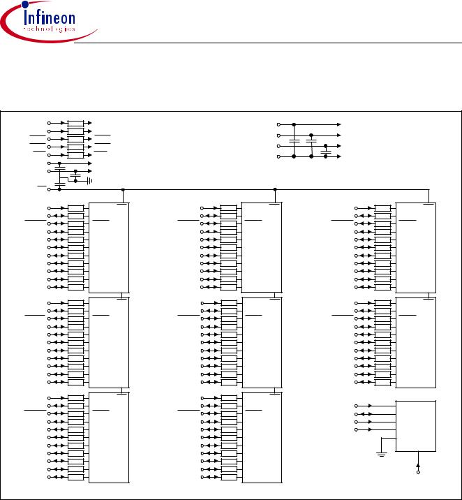
HYS[64T[3200/6400/12802]0/72T[6400/12802]0][G/H]U–[3.7/5]–A
512 Mbit DDR2 SDRAM
Block Diagrams
2 |
Block Diagrams |
|
|
|
|
|
|
|
|
|
|
|
|||||
|
|
|
|
|
|
|
|
|
|
|
|
|
|
|
|
||
|
|
|
||||||
|
|
|
|
|
|
|||
|
|
|
|
|
|
|
||
|
|
|
|
|
|
|||
|
|
|
|
|
|
|
|
|
|
|
|
|
|
|
|
|
|
|
|
|
|
|
|
|
|
|
|
|
|
|
|
|
|
|
|
|
|
|
|
|
|
|
|
|
|
|
|
|
|
|
|
|
|
|
! |
|
! |
|
|
|
! |
|
|
! |
|
! |
|
|
|
! |
|
|
! |
|
! |
|
|
|
|
! |
|
! |
|
! |
|
|
|
|
! |
|
! |
|
! |
|
|
|
|
! |
|
! |
|
! |
|
|
|
|
! |
|
! |
|
! |
|
|
|
|
! |
|
! |
|
! |
|
|
|
|
! |
|
|
|
|
|
|
|
|
|
|
|
|
|
|
|
|
|
|
|
|
|
|
|
|
|
|
|
|
! |
|
! |
|
|
|
|
! |
|
! |
|
! |
|
|
|
|
! |
|
! |
|
! |
|
|
|
|
! |
|
! |
|
! |
|
|
|
|
! |
|
! |
|
! |
|
|
|
! |
|
|
! |
|
! |
|
|
|
! |
|
|
! |
|
! |
|
|
|
! |
|
|
! |
|
! |
|
|
|
! |
|
|
|
|
|
# |
|
|
||
|
|
|
|
|
# |
|||
|
|
|
|
|
|
|
||
|
! |
|
! |
|
|
|
||
|
! |
|
! |
|
|
|
||
|
! |
|
! |
|
|
|
|
|
|
! |
|
! |
|
|
|
|
|
|
! |
|
! |
|
|
|
|
|
|
! |
|
! |
|
|
|
|
|
|
! |
|
! |
|
|
|
|
|
|
! |
|
! |
|
|
|
|
" |
|
|
|
|
|
|
|
|
|
Figure 3 Block Diagram Raw Card A UDIMM (×64, 1 Rank, ×8) |
|
|
|
|
|
|||
Note |
|
|
|
|
||||||||||||||
1. |
|
|
|
|
|
|
|
|
|
resistors are 22 Ω ± 5 % |
|
|
|
|
||||
DQ,DQS,DQS,DM |
|
Table 9 |
Clock Signal Loads |
|
||||||||||||||
2. |
BAn, An, |
RAS, |
|
CAS, |
|
WE |
resistors are 5.1 Ω ± 5 % |
|
|
|
|
|||||||
|
|
|
Clock Input |
|
SDRAMs |
Note |
||||||||||||
|
|
|
|
|
|
|
|
|
|
|
|
|
|
|
||||
3. |
ODT,CKE,S capacitors are 24 pF |
|||||||||||||||||
|
|
|
|
|||||||||||||||
CK0,CKO |
|
2 |
|
|||||||||||||||
4. |
All CK lines have resistor termination between CK |
|
|
|||||||||||||||
|
an |
|
|
|
|
|
|
|||||||||||
|
CK. |
CK1,CK1 |
|
3 |
|
|||||||||||||
|
|
|
|
|
|
|
|
|
|
|
|
|
|
|
|
|
|
|
|
|
|
|
|
|
|
|
|
|
|
|
|
|
CK2,CK3 |
|
3 |
|
|
|
|
|
|
|
|
|
|
|
|
|
|
|
|
|
|
|
|
|
Data Sheet |
18 |
Rev. 0.87, 2004-06 |
|
|
09122003-GZEK-H4J6 |

|
HYS[64T[3200/6400/12802]0/72T[6400/12802]0][G/H]U–[3.7/5]–A |
||||||||||||
|
|
|
|
|
|
|
|
|
512 Mbit DDR2 SDRAM |
||||
|
|
|
|
|
|
|
|
|
|
|
|
Block Diagrams |
|
|
|
|
|
|
|
|
|
|
|
|
# |
# |
|
|
|
|
|
|
|
|
|
|
|||||
|
|
|
|
|
|
|
|
|
|||||
|
|
|
|
|
|
|
|
|
|
||||
|
|
|
|
|
|
|
|
|
|
||||
|
|
|
|
|
|
|
|
|
|||||
|
|
|
|
||||||||||
|
|
|
|||||||||||
|
|
|
|
|
|
|
|
|
|
|
|||
|
|
|
|
|
|
|
|
||||||
|
|
|
|
|
|||||||||
|
|
|
|
|
|
||||||||
|
|
|
|
|
|
|
|
" |
|
||||
|
|
|
|
|
|
|
|
|
|
|
|
|
|
|
|
|
|
|
|
|
|
|
|||||
|
|
|
|
|
|
|
|
|
|
|
|||
|
|
|
|
|
|
|
|
|
|
|
|||
|
! |
|
|
! |
|
|
|
|
! |
|
|||
|
! |
|
|
|
! |
|
|
|
|
! |
|
||
|
! |
|
|
! |
|
|
|
|
|
! |
|
||
|
! |
|
|
! |
|
|
|
|
|
! |
|
||
|
! |
|
|
! |
|
|
|
|
|
! |
|
||
|
! |
|
|
! |
|
|
|
|
|
! |
|
||
|
! |
|
|
! |
|
|
|
|
|
! |
|
||
|
! |
|
|
! |
|
|
|
|
|
! |
|
||
|
|
|
|
|
|
|
|
|
|||||
|
|
|
|
|
|
|
|
|
|
|
|||
|
|
|
|
|
|
|
|
|
|
|
|||
|
! |
|
|
|
! |
|
|
|
|
|
! |
|
|
|
! |
|
|
|
! |
|
|
|
|
|
! |
|
|
|
! |
|
|
|
! |
|
|
|
|
|
! |
|
|
|
! |
|
|
|
|
! |
|
|
|
|
|
! |
|
|
! |
|
|
|
! |
|
|
|
|
! |
|
||
|
! |
|
|
|
! |
|
|
|
|
! |
|
||
|
! |
|
|
|
! |
|
|
|
|
! |
|
||
|
! |
|
|
|
! |
|
|
|
|
! |
|
||
|
|
|
|
|
|
|
|
|
|
||||
|
|
|
|
|
|
|
|
|
|
|
|
||
|
|
|
|
|
|
|
|
|
|
|
|
||
|
! |
|
|
|
! |
|
|
|
|
! |
|
||
|
! |
|
|
|
! |
|
|
|
|
! |
|
||
|
! |
|
|
|
! |
|
|
|
|
! |
|
||
|
! |
|
|
|
! |
|
|
|
|
! |
|
||
|
! |
|
|
|
! |
|
|
|
|
! |
|
||
|
! |
|
|
|
|
! |
|
|
|
|
! |
|
|
|
! |
|
|
|
! |
|
|
|
|
! |
|
||
|
! |
|
|
|
! |
|
|
|
|
! |
|
||
|
|
|
|
|
|
|
|
|
|
|
|
|
|
Figure 4 Block Diagram Raw Card A UDIMM (×72, 1 Rank, ×8)
Note
1.DQ,DQS,DQS,DM,CB resistors are 22 Ω ± 5 %
2.BAn, An, RAS, CAS, WE resistors are 5.1 Ω ± 5 %
3.ODT,CKE,S capacitors are 24 pF
4.All CK lines have resistor termination between CK an CK.
Table 10 Clock Signal Loads
Clock Input |
SDRAMs |
Note |
|||
|
|
|
|
|
|
|
|
|
|
1) |
|
CK0,CK0 |
3 |
||||
|
|||||
|
|
|
|
||
|
|
|
3 |
|
|
CK1,CK1 |
|
|
|||
|
|
|
|||
CK2,CK3 |
3 |
|
|||
|
|
|
|
|
|
1)2 SDRAMS for CK0 in case of non-ECC
Data Sheet |
19 |
Rev. 0.87, 2004-06 |
|
|
09122003-GZEK-H4J6 |
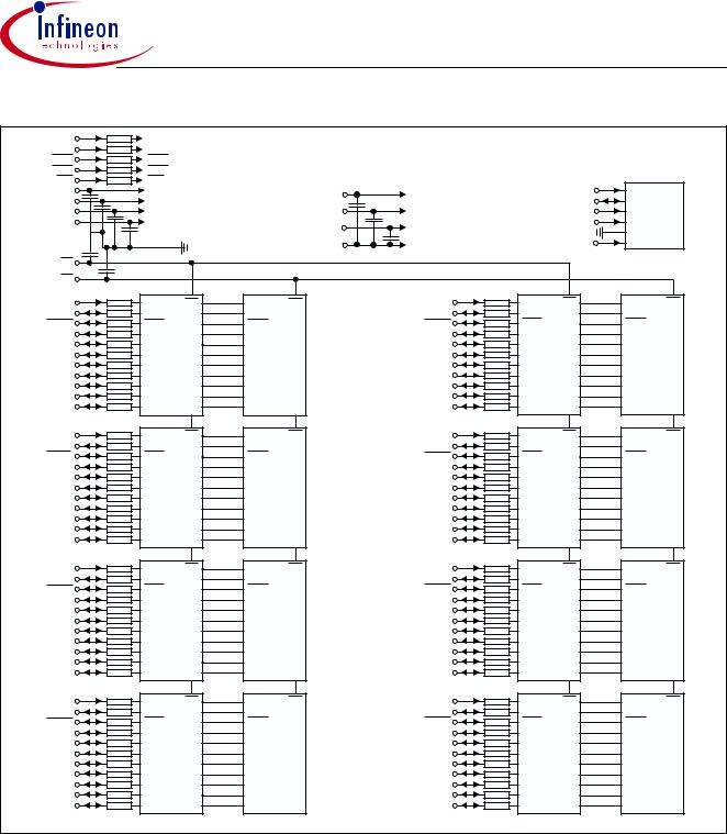
HYS[64T[3200/6400/12802]0/72T[6400/12802]0][G/H]U–[3.7/5]–A
512 Mbit DDR2 SDRAM
Block Diagrams
) |
|
|
|
|
|
|
|
|
|
|
BA0 - BA2 |
BA0 - BA2: SDRAMs D0 - D15 |
|
|
|
|
|
|
|||
A0 - An |
A0 - An: SDRAMs D0 - D15 |
|
|
|
|
|
|
|||
RAS |
RAS: SDRAMs D0 - D15 |
|
|
|
|
|
|
|||
CAS |
CAS: SDRAMs D0 - D15 |
|
|
|
|
|
|
|||
WE |
WE: SDRAMs D0 - D15 |
VDD,SPD |
|
|
|
|
E0 |
|||
CKE 0 |
CKE 0: SDRAMs D0 - D7 |
VDD: SPD EEPROM E0 |
SCL |
SCL |
|
|||||
CKE 1 |
CKE 1: SDRAMs D8 - D15 |
VDD/VDDQ |
SDA |
SDA |
|
|||||
VDD/VDDQ: SDRAMs D0 - D15 |
|
|||||||||
ODT 0 |
ODT 0: SDRAMs D0 - D7 |
VREF |
SA0 |
A0 |
|
|||||
VREF: SDRAMs D0 - D15 |
|
|||||||||
ODT 1 |
ODT 0: SDRAMs D8 - D15 |
VSS |
SA1 |
A1 |
|
|||||
|
|
|
|
|
VSS: SDRAMs D0 - D15 |
|
A2 |
|
||
|
|
V |
SS |
|
|
|
|
VSS |
WP |
|
S0 |
|
|
|
|
|
|
|
|
|
|
S1 |
|
|
|
|
|
|
|
|
|
|
|
|
|
D0 |
|
D8 |
|
|
D4 |
|
D12 |
DM0 |
DM |
CS |
DM |
CS |
DM4 |
DM |
CS |
DM |
CS |
|
DQS0 |
DQS |
|
|
DQS |
|
DQS4 |
DQS |
|
DQS |
|
DQS0 |
DQS |
|
|
DQS |
|
DQS4 |
DQS |
|
DQS |
|
DQ0 |
I/O 0 |
|
|
I/O 0 |
|
DQ32 |
I/O 0 |
|
I/O 0 |
|
DQ1 |
I/O 1 |
|
|
I/O 1 |
|
DQ33 |
I/O 1 |
|
I/O 1 |
|
DQ2 |
I/O 2 |
|
|
I/O 2 |
|
DQ34 |
I/O 2 |
|
I/O 2 |
|
DQ3 |
I/O 3 |
|
|
I/O 3 |
|
DQ35 |
I/O 3 |
|
I/O 3 |
|
DQ4 |
I/O 4 |
|
|
I/O 4 |
|
DQ36 |
I/O 4 |
|
I/O 4 |
|
DQ5 |
I/O 5 |
|
|
I/O 5 |
|
DQ37 |
I/O 5 |
|
I/O 5 |
|
DQ6 |
I/O 6 |
|
|
I/O 6 |
|
DQ38 |
I/O 6 |
|
I/O 6 |
|
DQ7 |
I/O 7 |
|
|
I/O 7 |
|
DQ39 |
I/O 7 |
|
I/O 7 |
|
|
|
|
D1 |
|
D9 |
|
|
D5 |
|
D13 |
DM1 |
DM |
CS |
DM |
CS |
DM5 |
DM |
CS |
DM |
CS |
|
DQS1 |
DQS |
|
|
DQS |
|
DQS5 |
DQS |
|
DQS |
|
DQS1 |
DQS |
|
|
DQS |
|
DQS5 |
DQS |
|
DQS |
|
DQ8 |
I/O 0 |
|
|
I/O 0 |
|
DQ40 |
I/O 0 |
|
I/O 0 |
|
DQ9 |
I/O 1 |
|
|
I/O 1 |
|
DQ41 |
I/O 1 |
|
I/O 1 |
|
DQ10 |
I/O 2 |
|
|
I/O 2 |
|
DQ42 |
I/O 2 |
|
I/O 2 |
|
DQ11 |
I/O 3 |
|
|
I/O 3 |
|
DQ43 |
I/O 3 |
|
I/O 3 |
|
DQ12 |
I/O 4 |
|
|
I/O 4 |
|
DQ44 |
I/O 4 |
|
I/O 4 |
|
DQ13 |
I/O 5 |
|
|
I/O 5 |
|
DQ45 |
I/O 5 |
|
I/O 5 |
|
DQ14 |
I/O 6 |
|
|
I/O 6 |
|
DQ46 |
I/O 6 |
|
I/O 6 |
|
DQ15 |
I/O 7 |
|
|
I/O 7 |
|
DQ47 |
I/O 7 |
|
I/O 7 |
|
|
|
|
D2 |
|
D10 |
|
|
D6 |
|
D14 |
DM2 |
DM |
CS |
DM |
CS |
DM6 |
DM |
CS |
DM |
CS |
|
DQS2 |
DQS |
|
|
DQS |
|
DQS6 |
DQS |
|
DQS |
|
DQS2 |
DQS |
|
|
DQS |
|
DQS6 |
DQS |
|
DQS |
|
DQ16 |
I/O 0 |
|
|
I/O 0 |
|
DQ48 |
I/O 0 |
|
I/O 0 |
|
DQ17 |
I/O 1 |
|
|
I/O 1 |
|
DQ49 |
I/O 1 |
|
I/O 1 |
|
DQ18 |
I/O 2 |
|
|
I/O 2 |
|
DQ50 |
I/O 2 |
|
I/O 2 |
|
DQ19 |
I/O 3 |
|
|
I/O 3 |
|
DQ51 |
I/O 3 |
|
I/O 3 |
|
DQ20 |
I/O 4 |
|
|
I/O 4 |
|
DQ52 |
I/O 4 |
|
I/O 4 |
|
DQ21 |
I/O 5 |
|
|
I/O 5 |
|
DQ53 |
I/O 5 |
|
I/O 5 |
|
DQ22 |
I/O 6 |
|
|
I/O 6 |
|
DQ54 |
I/O 6 |
|
I/O 6 |
|
DQ23 |
I/O 7 |
|
|
I/O 7 |
|
DQ55 |
I/O 7 |
|
I/O 7 |
|
|
|
|
D3 |
|
D11 |
|
|
D7 |
|
D15 |
DM3 |
DM |
CS |
DM |
CS |
DM7 |
DM |
CS |
DM |
CS |
|
DQS3 |
DQS |
|
|
DQS |
|
DQS7 |
DQS |
|
DQS |
|
DQS3 |
DQS |
|
|
DQS |
|
DQS7 |
DQS |
|
DQS |
|
DQ24 |
I/O 0 |
|
|
I/O 0 |
|
DQ56 |
I/O 0 |
|
I/O 0 |
|
DQ25 |
I/O 1 |
|
|
I/O 1 |
|
DQ57 |
I/O 1 |
|
I/O 1 |
|
DQ26 |
I/O 2 |
|
|
I/O 2 |
|
DQ58 |
I/O 2 |
|
I/O 2 |
|
DQ27 |
I/O 3 |
|
|
I/O 3 |
|
DQ59 |
I/O 3 |
|
I/O 3 |
|
DQ28 |
I/O 4 |
|
|
I/O 4 |
|
DQ60 |
I/O 4 |
|
I/O 4 |
|
DQ29 |
I/O 5 |
|
|
I/O 5 |
|
DQ61 |
I/O 5 |
|
I/O 5 |
|
DQ30 |
I/O 6 |
|
|
I/O 6 |
|
DQ62 |
I/O 6 |
|
I/O 6 |
|
DQ31 |
I/O 7 |
|
|
I/O 7 |
|
DQ63 |
I/O 7 |
|
I/O 7 |
|
|
|
|
|
|
|
|
|
|
|
MPBT0130 |
Figure 5 |
Block Diagram Raw Card B UDIMM (×64, 1 Rank, ×8) |
|
|
|
|
|||||
Note |
|
|
|
|
|
|||||||||||||
1. |
|
|
|
|
|
|
|
|
|
|
|
|
|
|
|
|
|
|
DQ,DQS,DQS,DM,CB resistors are 22 Ω ± 5 % |
|
|
|
|
|
|||||||||||||
2. |
BAn, An, |
RAS, |
|
CAS, |
|
WE |
resistors are 7.5 Ω ± 5 % |
Table 11 Clock Signal Loads |
|
|||||||||
|
|
|
|
|
|
|
|
|
|
|
|
|
|
|
||||
3. |
ODT,CKE,S capacitors are 24 pF |
|
||||||||||||||||
|
|
|
|
|
||||||||||||||
4. |
All CK lines have resistor termination between CK |
Clock Input |
SDRAMs |
Note |
||||||||||||||
|
an |
CK. |
|
|
|
|
4 |
|
||||||||||
|
|
|
|
|
|
|
|
|
|
|
|
CK0,CK0 |
|
|
||||
|
|
|
|
|
|
|
|
|
|
|
|
|
|
|
|
|
|
|
|
|
|
|
|
|
|
|
|
|
|
|
|
|
|
|
|
6 |
|
|
|
|
|
|
|
|
|
|
|
|
|
|
|
CK1,CK1 |
|
|
||
|
|
|
|
|
|
|
|
|
|
|
|
|
|
|
|
|
||
|
|
|
|
|
|
|
|
|
|
|
|
|
|
CK2,CK3 |
6 |
|
||
|
|
|
|
|
|
|
|
|
|
|
|
|
|
|
|
|
|
|
Data Sheet |
20 |
Rev. 0.87, 2004-06 |
|
|
09122003-GZEK-H4J6 |
HYS[64T[3200/6400/12802]0/72T[6400/12802]0][G/H]U–[3.7/5]–A
512 Mbit DDR2 SDRAM
Block Diagrams
|
|
|
|
|
|
|
|||||
|
|
|
|
|
|
|
|
||||
|
|
|
|
|
|
|
|
||||
|
|
|
|
|
|
|
|
||||
|
|
|
|
|
|
|
|
|
|||
|
|
|
|
|
|
|
|
|
|
|
|
|
|
|
|
|
|
|
|
|
|
|
|
|
|
|
|
|
|
|
|
|
|
|
|
|
|
|
|
|
|
|
|
||||
|
|
|
|
|
|
|
|
|
|
||
|
|
|
|
|
|
|
|
|
|
||
|
! |
! |
|
|
|
|
! |
! |
|
||
|
! |
! |
|
|
|
|
! |
! |
|
||
|
! |
! |
|
|
|
|
! |
! |
|
||
|
! |
! |
|
|
|
|
|
|
! |
! |
|
|
! |
! |
|
|
|
|
! |
! |
|
||
|
! |
! |
|
|
|
|
! |
! |
|
||
|
! |
! |
|
|
|
|
! |
! |
|
||
|
! |
! |
|
|
|
|
! |
! |
|
||
|
|
|
|
|
|
|
|
|
|
||
|
|
|
|
|
|
|
|
|
|
|
|
|
|
|
|
|
|
|
|
|
|
|
|
|
! |
! |
|
|
|
|
! |
! |
|
||
|
! |
! |
|
|
|
|
! |
! |
|
||
|
! |
! |
|
|
|
|
! |
! |
|
||
|
! |
! |
|
|
|
|
! |
! |
|
||
|
! |
! |
|
|
|
|
! |
! |
|
||
|
! |
! |
|
|
|
|
|
|
! |
! |
|
|
! |
! |
|
|
|
|
! |
! |
|
||
|
! |
! |
|
|
|
|
! |
! |
|
||
|
|
|
|
|
|
|
|
||||
|
|
|
|
|
|
|
|
|
|
||
|
|
|
|
|
|
|
|
|
|
||
|
! |
! |
|
|
|
|
! |
! |
|
||
|
! |
! |
|
|
|
|
! |
! |
|
||
|
! |
! |
|
|
|
|
|
! |
! |
|
|
|
! |
! |
|
|
|
|
|
! |
! |
|
|
|
! |
! |
|
|
|
|
|
! |
! |
|
|
|
! |
! |
|
|
|
|
|
! |
! |
|
|
|
! |
! |
|
|
|
|
|
! |
! |
|
|
|
! |
! |
|
|
|
|
|
|
! |
! |
|
|
|
|
|
|
|
|
|
||||
|
|
|
|
|
|
|
|
|
|
||
|
|
|
|
|
|
|
|
|
|
||
|
! |
! |
|
|
|
|
|
! |
! |
|
|
|
! |
! |
|
|
|
|
|
! |
! |
|
|
|
! |
! |
|
|
|
|
|
! |
! |
|
|
|
! |
! |
|
|
|
|
|
! |
! |
|
|
|
! |
! |
|
|
|
|
! |
! |
|
||
|
! |
! |
|
|
|
|
! |
! |
|
||
|
! |
! |
|
|
|
|
! |
! |
|
||
|
! |
! |
|
|
|
|
! |
! |
|
||
|
|
|
|
|
|
|
|
# |
# |
|
|
|
|
|
|
|
|
||||||
|
|
|
|
|
|
|
|
|
|
|
|
|
|
|
|
|
|
|
|
|
|
|
|
|
! |
! |
|
|
|
|
|
|
|
|
|
|
! |
! |
|
|
|
|
|
|
|
|
|
|
! |
! |
|
|
|
|
|
|
|
|
|
|
! |
! |
|
|
|
|
|
||||
|
! |
! |
|
|
|
|
|
|
|
|
|
|
|
|
|
|
" |
|
|||||
|
! |
! |
|
|
|
|
|
|
|
|
|
|
! |
! |
|
|
|
||||||
|
! |
! |
|
|
|
|
|||||
|
|
|
|
|
|
|
|
|
|
|
|
Figure 6 Block Diagram Raw Card B UDIMM (×72, 1 Rank, ×8) |
|
|
|
|
|||||||
Note: |
|
|
|
|
|
|
|
|
|
|
|
1. DQ,DQS,DQS,DM,CB resistors are 22 Ω ± 5 % |
Table 12 Clock Signal Loads |
|
|
||||||||
2. BAn, An, RAS, CAS, WE resistors are 7.5 Ω ± 5 % |
Clock Input |
SDRAMs |
Note |
|
|||||||
3. ODT,CKE,S capacitors are 24 pF |
|
|
|||||||||
|
CK0,CK0 |
|
6 |
|
|
||||||
4. All CK lines have resistor termination between CK |
|
|
|
||||||||
CK1,CK1 |
|
6 |
|
|
|||||||
an CK. |
|
|
|
|
|
|
|||||
|
|
|
|
CK2,CK3 |
|
6 |
|
|
|||
Data Sheet |
21 |
Rev. 0.87, 2004-06 |
|
|
09122003-GZEK-H4J6 |
Loading...