


Data Sheet, Dec. 2000
C505
C505C
C505A
C505CA
8-Bit Single-Chip Microcontroller
Microcontrollers
N e v e r s t o p t h i n k i n g .
Edition 2000-12
Published by Infineon Technologies AG, St.-Martin-Strasse 53,
D-81541 München, Germany
© Infineon Technologies AG 2000. All Rights Reserved.
Attention please!
The information herein is given to describe certain components and shall not be considered as warranted characteristics.
Terms of delivery and rights to technical change reserved.
We hereby disclaim any and all warranties, including but not limited to warranties of non-infringement, regarding circuits, descriptions and charts stated herein.
Infineon Technologies is an approved CECC manufacturer.
Information
For further information on technology, delivery terms and conditions and prices please contact your nearest Infineon Technologies Office in Germany or our Infineon Technologies Representatives worldwide (see address list).
Warnings
Due to technical requirements components may contain dangerous substances. For information on the types in question please contact your nearest Infineon Technologies Office.
Infineon Technologies Components may only be used in life-support devices or systems with the express written approval of Infineon Technologies, if a failure of such components can reasonably be expected to cause the failure of that life-support device or system, or to affect the safety or effectiveness of that device or system. Life support devices or systems are intended to be implanted in the human body, or to support and/or maintain and sustain and/or protect human life. If they fail, it is reasonable to assume that the health of the user or other persons may be endangered.

Data Sheet, Dec. 2000
C505
C505C
C505A
C505CA
8-Bit Single-Chip Microcontroller
Microcontrollers
N e v e r s t o p t h i n k i n g .

C505/C505C/C505A/C505CA Data Sheet
Revision History : |
Current Version : 2000-12 |
|
Previous Releases : |
08.00, 06.00, 07.99, 12.97 |
|
|
|
|
Page |
Page |
Subjects (major changes since last revision) |
(in previous |
(in current |
|
version |
version) |
|
|
|
|
24 |
24 |
Version register VR2 for C505A-4R/C505CA-4R BB step is updated. |
|
|
|
|
|
|
|
|
|
Controller Area Network (CAN): License of Robert Bosch GmbH
We Listen to Your Comments
Any information within this document that you feel is wrong, unclear or missing at all? Your feedback will help us to continuously improve the quality of this document. Please send your proposal (including a reference to this document) to: 

mcdocu.comments@infineon.com
8-Bit Single-Chip Microcontroller |
C505/C505C/C505A/ |
C500 Family |
C505CA |
Advance Information
•Fully compatible to standard 8051 microcontroller
•Superset of the 8051 architecture with 8 datapointers
•Up to 20 MHz operating frequency
–375 ns instruction cycle time @16 MHz
–300 ns instruction cycle time @20 MHz (50 % duty cycle)
•On-chip program memory (with optional memory protection)
– C505(C)(A)-2R : |
16K byte on-chip ROM |
–C505A-4R/C505CA-4R: 32K byte on-chip ROM
–C505A-4E/C505CA-4E: 32K byte on-chip OTP
–alternatively up to 64k byte external program memory
•256 byte on-chip RAM
•On-chip XRAM
–C505/C505C : 256 byte
–C505A/C505CA : 1K byte
(more features on next page)
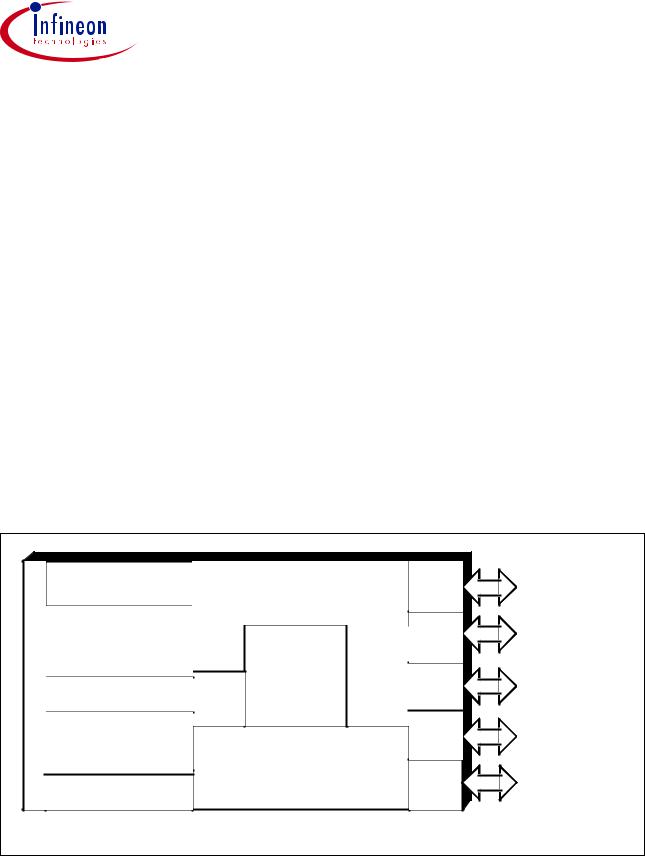
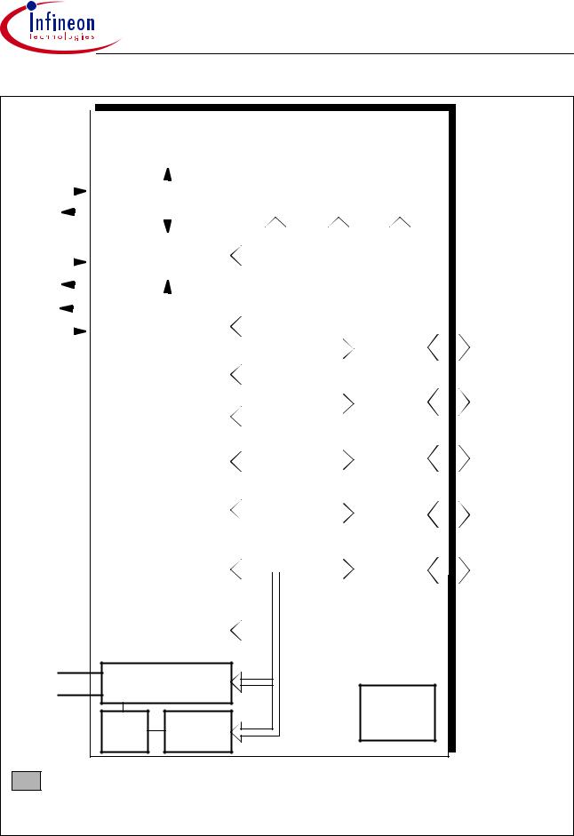
On-Chip Emulation Support Module
Oscillator |
|
XRAM |
RAM |
Port 0 |
I/O |
|
Watchdog |
C505/C505C: 256 byte |
|||||
|
||||||
|
256 byte |
|
|
|||
A/D Converter |
C505A/C505CA: 1K byte |
|
|
|||
Timer |
|
|
Port 1 |
8 analog inputs / |
||
C505/C505C : 8-bit |
C500 |
|
8 digit. I/O |
|||
8-bit |
|
|||||
C505A/C505CA : 10-bit |
0 |
Core |
|
|
||
|
USART |
|
|
|||
|
|
|
Port 2 |
I/O |
||
Timer 2 |
Timer |
8 Datapointers |
|
|||
|
|
|
||||
|
1 |
|
|
|
|
|
Full-CAN Controller |
|
Program Memory |
Port 3 |
I/O |
||
C505C/C505CA only |
|
|
|
|||
|
C505(C)(A)-2R : 16K ROM |
|
|
|||
|
|
|
I/O (2-bit I/O port) |
|||
Watchdog Timer |
C505A-4R/C505CA-4R : 32K ROM |
Port 4 |
||||
C505A-4E/C505CA-4E : 32K OTP |
|
|
||||
|
|
|
||||
Figure 1
C505 Functional Units
Data Sheet |
1 |
12.00 |
C505/C505C/C505A/C505CA
Features (continued) :
•32 + 2 digital I/O lines
–Four 8-bit digital I/O ports
–One 2-bit digital I/O port (port 4)
–Port 1 with mixed analog/digital I/O capability
•Three 16-bit timers/counters
–Timer 0 / 1 (C501 compatible)
–Timer 2 with 4 channels for 16-bit capture/compare operation
•Full duplex serial interface with programmable baudrate generator (USART)
•Full CAN Module, version 2.0 B compliant (C505C and C505CA only)
–256 register/data bytes located in external data memory area
–1 MBaud CAN baudrate when operating frequency is equal to or above 8 MHz
–internal CAN clock prescaler when input frequency is over 10 MHz
•On-chip A/D Converter
–up to 8 analog inputs
– C505/C505C : 8-bit resolution
–C505A/C505CA: 10-bit resolution
•Twelve interrupt sources with four priority levels
•On-chip emulation support logic (Enhanced Hooks Technology TM)
•Programmable 15-bit watchdog timer
•Oscillator watchdog
•Fast power on reset
•Power Saving Modes
–Slow-down mode
–Idle mode (can be combined with slow-down mode)
–Software power-down mode with wake up capability through P3.2/INT0 or P4.1/RXDC pin
•P-MQFP-44 package
•Pin configuration is compatible to C501, C504, C511/C513-family
•Temperature ranges:
SAB-C505 versions SAF-C505 versions SAH-C505 versions SAK-C505 versions
TA = 0 to 70 ° C TA = -40 to 85° C TA = -40 to 110° C TA = -40 to 125° C
Data Sheet |
2 |
12.00 |

C505/C505C/C505A/C505CA
Table 1
Differences in Functionality of the C505 MCUs
Device |
Internal Program Memory |
XRAM Size |
A/D Converter |
CAN |
|
|
|
|
|
Resolution |
Controller |
|
ROM |
OTP |
|
||
|
|
|
|
||
|
|
|
|
|
|
C505-2R |
16K byte |
– |
256 byte |
8 Bit |
– |
|
|
|
|
|
|
C505-L |
– |
– |
256 byte |
8 Bit |
– |
|
|
|
|
|
|
C505C-2R |
16K byte |
– |
256 byte |
8 Bit |
√ |
|
|
|
|
|
|
C505C-L |
– |
– |
256 byte |
8 Bit |
√ |
|
|
|
|
|
|
C505A-4R |
32K byte |
– |
1K byte |
10 Bit |
– |
|
|
|
|
|
|
C505A-2R |
16K byte |
– |
1K byte |
10 Bit |
– |
|
|
|
|
|
|
C505A-L |
– |
– |
1K byte |
10 Bit |
– |
|
|
|
|
|
|
C505CA-4R |
32K byte |
– |
1K byte |
10 Bit |
√ |
|
|
|
|
|
|
C505CA-2R |
16K byte |
– |
1K byte |
10 Bit |
√ |
|
|
|
|
|
|
C505CA-L |
– |
– |
1K byte |
10 Bit |
√ |
|
|
|
|
|
|
C505A-4E |
– |
32K byte |
1K byte |
10 Bit |
– |
|
|
|
|
|
|
C505CA-4E |
– |
32K byte |
1K byte |
10 Bit |
√ |
|
|
|
|
|
|
Note: The term C505 refers to all versions described within this document unless otherwise noted. However the term C505 may also be restricted by the context to refer to only CAN-less derivatives with 8-Bit ADC which are C505-2R and C505-L in this document.
Note: The term C505(C)(A)-2R, for simplicity, is used to stand for C505 16K byte ROM versions within this document which are C505-2R, C505C-2R, C505A-2R and C505CA-2R.
Ordering Information
The ordering code for Infineon Technologies’ microcontrollers provides an exact reference to the required product. This ordering code identifies:
•the derivative itself, i.e. its function set
•the specificed temperature rage
•the package and the type of delivery
For the available ordering codes for the C505 please refer to the “Product information Microcontrollers”, which summarizes all available microcontroller variants.
Data Sheet |
3 |
12.00 |
C505/C505C/C505A/C505CA
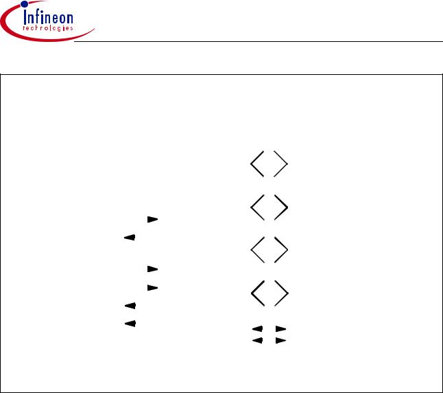
VDD VSS
|
VAREF |
|
|
|
|
|
|
|
|
|
|
|
|
Port 0 |
|||
|
|
|
|
|
|
|
|
|
|
|
|
|
|||||
|
|
|
|
|
|
|
|
|
|
|
|
|
|||||
|
|
|
|
|
|
|
|
|
|
|
|
||||||
|
|
|
|
|
|
|
|
|
|
|
8-bit Digital I/O |
||||||
|
|
|
|
|
|
|
|
|
|
||||||||
|
VAGND |
|
|
|
|
|
|
|
|
|
|
|
Port 1 |
||||
|
|
|
|
|
|
|
|
|
|
|
|
||||||
|
|
|
|
|
|
|
|
|
|
|
|
|
|
|
|
|
|
|
|
|
|
|
|
|
|
|
|
|
|
|
|
|
|
||
XTAL1 |
|
|
|
|
|
|
|
|
|
|
|
8-bit Digital I/O / |
|||||
|
|
|
|
|
|
|
|
|
|
||||||||
|
|
|
|
C505 |
|
|
|
|
8-bit Analog Inputs |
||||||||
XTAL2 |
|
|
|
|
|
|
|
|
|||||||||
|
|
|
|
C505C |
|
|
|
|
Port 2 |
||||||||
|
|
|
|
|
|
|
|||||||||||
|
|
|
|
|
|
|
|
|
|
|
C505A |
|
|
|
|
||
|
|
|
|
|
|
|
|
|
|
|
|
|
|
|
8-bit Digital I/O |
||
RESET |
|
|
|
|
C505CA |
|
|
|
|
||||||||
|
|
|
|
|
|
|
|
Port 3 |
|||||||||
|
|
|
|
|
|
|
|
|
|
|
|||||||
|
|
|
|
|
|
|
|
|
|
|
|
|
|
|
|
|
|
|
|
EA |
|
|
|
|
|
|
|
|
|
|
|
|
|
|
|
|
|
|
|
|
|
|
|
|
|
|
|
|
|
|
|||
|
ALE |
|
|
|
|
|
|
|
|
|
8-bit Digital I/O |
||||||
|
|
|
|
|
|
|
|
|
|||||||||
|
|
|
|
|
|
|
|
|
|
|
|||||||
|
|
|
|
|
|
|
|
|
|
||||||||
|
|
|
|
|
|
|
|
|
|
|
|
|
|
|
|
|
|
PSEN |
|
|
|
|
|
|
|
|
|
Port 4 |
|||||||
|
|
|
|
|
|
|
|
|
|
|
|
|
|
|
|||
|
|
|
|
|
|
|
|
|
|
|
|
|
|
|
|
|
|
|
|
|
|
|
|
|
|
|
|
|
|
|
|
|
|
|
2-bit Digital I/O |
|
|
|
|
|
|
|
|
|
|
|
|
|
|
|
|
|
|
|
|
|
|
|
|
|
|
|
|
|
|
|
|
|
|
|
|
Figure 2
Logic Symbol
Note: The ordering codes for the Mask-ROM versions are defined for each product after verification of the respective ROM code.
Data Sheet |
4 |
12.00 |
C505/C505C/C505A/C505CA
P0.3 / AD3
P0.2 / AD2
P0.1 / AD1
P0.0 / AD0
V AREF
V AGND
P1.0 / AN0 / INT3 / CC0
P1.1 / AN1 / INT4 / CC1
P1.2 / AN2 / INT5 / CC2
P1.3 / AN3 / INT6 / CC3
P1.4 / AN4
|
P0.4 / AD4 |
P0.5 / AD5 |
P0.6 / AD6 |
P0.7 / AD7 |
|
|
|
RXDC |
|
|
|
PSEN |
P2.7 / A15 |
P2.6 / A14 |
P2.5 / A13 |
|
|
|
|
|
|
|
|
|
|||||||||||||||||
|
EA |
P4.1 / |
ALE |
|
|
|
|
|
|
|
|
|
|||||||||||||||||||||||||||||
|
|
|
|
|
|
|
|
|
|
||||||||||||||||||||||||||||||||
|
|
|
|
|
|
|
|
|
|
|
|
|
|
|
|
|
|
|
|
|
|
|
|
|
|
|
|
|
|
|
|
|
|
||||||||
|
|
|
|
|
|
|
|
|
|
|
|
|
|
|
|
|
|
|
|
|
|
|
|
|
|
|
|
|
|
|
|
|
|
|
|
|
|
|
|
|
|
|
|
|
|
|
|
|
|
|
|
|
|
|
|
|
|
|
|
|
|
|
|
|
|
|
|
|
|
|
|
|
|
|
|
|
|
|
|
|
|
|
|
|
|
|
|
|
|
|
|
|
|
|
|
|
|
|
|
|
|
|
|
|
|
|
|
|
|
|
|
|
|
|
|
|
|
|
|
|
|
|
|
|
|
33 32 31 30 29 28 27 26 25 24 23 |
|
|
|
|
P2.4 |
/ A12 |
|||||||||||||||||||||||||||||||||||
|
|
|
|
||||||||||||||||||||||||||||||||||||||
34 |
|
|
|
|
|
|
|
|
|
|
|
|
|
|
|
|
|
|
|
|
|
|
|
|
|
|
|
|
|
22 |
|
|
|
|
|||||||
|
|
|
|
|
|
|
|
|
|
|
|
|
|
|
|
|
|
|
|
|
|
|
|
|
|
|
|
|
|
|
|
|
|||||||||
35 |
|
|
|
|
|
|
|
|
|
|
|
|
|
|
|
|
|
|
|
|
|
|
|
|
|
|
|
|
|
21 |
|
|
|
|
P2.3 |
/ A11 |
|||||
|
|
|
|
|
|
|
|
|
|
|
|
|
|
|
|
|
|
|
|
|
|
|
|
|
|
|
|
|
|
|
|
|
|||||||||
|
|
|
|
|
|
|
|
|
|
|
|
|
|
|
|
|
|
|
|
|
|
|
|
|
|
|
|
|
|
|
|
|
|||||||||
36 |
|
|
|
|
|
|
|
|
|
|
|
|
|
|
|
|
|
|
|
|
|
|
|
|
|
|
|
|
|
20 |
|
|
|
|
P2.2 |
/ A10 |
|||||
|
|
|
|
|
|
|
|
|
|
|
|
|
|
|
|
|
|
|
|
|
|
|
|
|
|
|
|
|
|
|
|
|
|||||||||
|
|
|
|
|
|
|
|
|
|
|
|
|
|
|
|
|
|
|
|
|
|
|
|
|
|
|
|
|
|
|
|
|
|||||||||
37 |
|
|
|
|
|
|
|
|
|
|
|
|
C505 |
|
|
|
|
|
|
|
|
|
19 |
|
|
|
|
P2.1 |
/ A9 |
||||||||||||
|
|
|
|
|
|
|
|
|
|
|
|
|
|
|
|
|
|
|
|
|
|
|
|
|
|||||||||||||||||
|
|
|
|
|
|
|
|
|
|
|
|
|
|
|
|
|
|
|
|
|
|
|
|
|
|||||||||||||||||
38 |
|
|
|
|
|
|
|
|
|
|
|
C505C |
|
|
|
|
|
|
|
|
|
18 |
|
|
|
|
P2.0 |
/ A8 |
|||||||||||||
|
|
|
|
|
|
|
|
|
|
|
|
|
|
|
|
|
|
|
|
|
|
|
|
||||||||||||||||||
|
|
|
|
|
|
|
|
|
|
|
|
|
|
|
|
|
|
|
|
|
|
|
|
||||||||||||||||||
39 |
|
|
|
|
|
|
|
|
|
|
|
C505A |
|
|
|
|
|
|
|
|
|
17 |
|
|
|
|
V DD |
|
|
|
|
||||||||||
|
|
|
|
|
|
|
|
|
|
|
|
|
|
|
|
|
|
|
|
|
|
|
|
|
|
|
|
||||||||||||||
|
|
|
|
|
|
|
|
|
|
|
|
|
|
|
|
|
|
|
|
|
|
|
|
|
|
|
|
||||||||||||||
40 |
|
|
|
|
|
|
|
|
|
|
C505CA |
|
|
|
|
|
|
|
|
|
16 |
|
|
|
|
V SS |
|
|
|
|
|||||||||||
|
|
|
|
|
|
|
|
|
|
|
|
|
|
|
|
|
|
|
|
|
|
|
|
|
|
|
|||||||||||||||
41 |
|
|
|
|
|
|
|
|
|
|
|
|
|
|
|
|
|
|
|
15 |
|
|
|
|
XTAL1 |
||||||||||||||||
|
|
|
|
|
|
|
|
|
|
|
|
|
|
|
|
|
|
|
|
|
|
|
|
|
|
|
|
|
|
|
|
|
|||||||||
42 |
|
|
|
|
|
|
|
|
|
|
|
|
|
|
|
|
|
|
|
|
|
|
|
|
|
|
|
|
|
14 |
|
|
|
|
XTAL2 |
||||||
|
|
|
|
|
|
|
|
|
|
|
|
|
|
|
|
|
|
|
|
|
|
|
|
|
|
|
|
|
|
|
|
|
|||||||||
|
|
|
|
|
|
|
|
|
|
|
|
|
|
|
|
|
|
|
|
|
|
|
|
|
|
|
|
|
|
|
|
|
|||||||||
|
|
|
|
|
|
|
|
|
|
|
|
|
|
|
|
|
|
|
|
|
|
|
|
|
|
|
|
|
|
|
|
|
|
|
|
|
P3.7 |
/ |
|
|
|
43 |
|
|
|
|
|
|
|
|
|
|
|
|
|
|
|
|
|
|
|
|
|
|
|
|
|
|
|
|
|
13 |
RD |
||||||||||
|
|
|
|
|
|
|
|
|
|
|
|
|
|
|
|
|
|
|
|
|
|
|
|
|
|
|
|
|
|
|
|
|
|
|
|||||||
|
|
|
|
|
|
|
|
|
|
|
|
|
|
|
|
|
|
|
|
|
|
|
|
|
|
|
|
|
|
|
|
|
|
|
|||||||
|
|
|
|
|
|
|
|
|
|
|
|
|
|
|
|
|
|
|
|
|
|
|
|
|
|
|
|
|
|
|
|
|
|
|
|
|
P3.6 |
/ |
|
|
|
44 |
|
|
|
|
|
|
|
|
|
|
|
|
|
|
|
|
|
|
|
|
|
|
|
|
|
|
|
|
|
12 |
WR |
||||||||||
|
|
|
|
|
|
|
|
|
|
|
|
|
|
|
|
|
|
|
|
|
|
|
|
|
|
|
|
|
|
|
|
|
|
||||||||
|
|
|
|
|
|
|
|
|
|
|
|
|
|
|
|
|
|
|
|
|
|
|
|
|
|
|
|
|
|
|
|
|
|
||||||||
1 |
|
2 |
|
3 |
|
4 |
|
5 |
|
6 |
|
7 |
|
8 |
|
9 |
|
10 11 |
|
|
|
|
|
|
|
|
|
||||||||||||||
|
|
|
|
|
|
|
|
|
|
|
|
|
|
|
|
|
|
|
|
|
|
|
|
|
|
|
|
|
|
|
|
|
|
|
|
|
|
|
|
|
|
|
|
|
|
|
|
|
|
|
|
|
|
|
|
|
|
|
|
|
|
|
|
|
|
|
|
|
|
|
|
|
|
|
|
|
|
|
|
|
|
|
|
|
|
|
|
|
|
|
|
|
|
|
|
|
|
|
|
|
|
|
|
|
|
|
|
|
|
|
|
|
|
|
|
|
|
|
|
|
|
|
|
|
|
|
|
|
|
|
|
|
|
|
|
|
|
|
|
|
|
|
|
|
|
|
|
|
|
|
|
|
|
|
|
|
|
|
|
|
|
|
|
|
|
|
|
|
|
|
|
|
|
|
|
|
|
|
RESET |
|
|
|
|
|
|
|
|
|
|
|
|
|
|
|
|
|
|
|
|
|
|
|
|
|
|
|
|
|
|
|
|
|
|
|
|
|
|
|
|
TXDC |
|
|
|
|
|
|
|
|
|
|
|
|
|
|
|
|
|
|
|||||||||||||
|
|
P1.5 / AN5 / T2EX |
|
P1.6 / AN6 / CLKOUT |
|
P1.7 / AN7 / T2 |
|
|
P3.0 / RxD |
|
P3.1 / TxD |
|
P3.2 / INT0 |
|
P3.3 / INT1 |
|
P3.4 / T0 |
P3.5 / T1 |
|
|
|
|
|
|
|
|
|
||||||||||||||
|
|
|
|
|
|
|
|
|
|
|
|
|
|
|
|
|
|
|
|||||||||||||||||||||||
P4.0 / |
|
|
|
|
|
|
|
|
|
||||||||||||||||||||||||||||||||
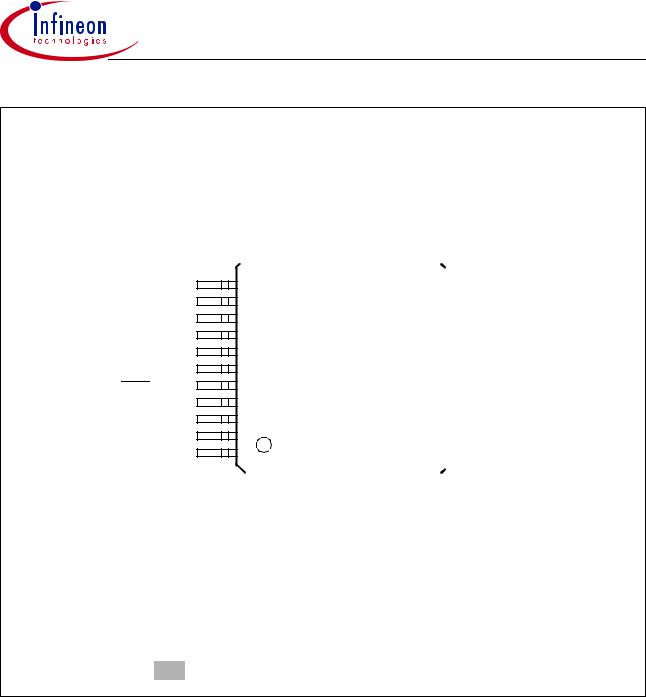
This pin functionality is not available in the C505/C505A.
Figure 3
C505 Pin Configuration P-MQFP-44 Package (Top View)
Data Sheet |
5 |
12.00 |

C505/C505C/C505A/C505CA
Table 2
Pin Definitions and Functions
Symbol |
|
Pin Number |
I/O |
Function |
|
||
|
|
|
*) |
|
|
|
|
|
|
|
|
|
|
||
P1.0-P1.7 |
|
40-44,1-3 |
I/O |
Port 1 |
|
||
|
|
|
|
is an 8-bit quasi-bidirectional port with internal pull-up |
|||
|
|
|
|
arrangement. Port 1 pins can be used for digital input/output |
|||
|
|
|
|
or as analog inputs of the A/D converter. Port 1 pins that |
|||
|
|
|
|
have 1’s written to them are pulled high by internal pull-up |
|||
|
|
|
|
transistors and in that state can be used as inputs. As |
|||
|
|
|
|
inputs, port 1 pins being externally pulled low will source |
|||
|
|
|
|
current (IIL, in the DC characteristics) because of the |
|||
|
|
|
|
internal pullup transistors. Port 1 pins are assigned to be |
|||
|
|
|
|
used as analog inputs via the register P1ANA. |
|||
|
|
|
|
As secondary digital functions, port 1 contains the interrupt, |
|||
|
|
|
|
timer, clock, capture and compare pins. The output latch |
|||
|
|
|
|
correspondi ng to a secondary function must be |
|||
|
|
|
|
programmed to a one (1) for that function to operate (except |
|||
|
|
|
|
for compare functions). The secondary functions are |
|||
|
|
|
|
assigned to the pins of port 1 as follows: |
|||
|
|
40 |
|
P1.0 / AN0 / |
|
/ CC0 |
Analog input channel 0 |
|
|
|
INT3 |
||||
|
|
|
|
|
|
|
interrupt 3 input / |
|
|
|
|
|
|
|
capture/compare channel 0 I/O |
|
|
41 |
|
P1.1 / AN1 / INT4 / CC1 |
Analog input channel 1/ |
||
|
|
|
|
|
|
|
interrupt 4 input / |
|
|
|
|
|
|
|
capture/compare channel 1 I/O |
|
|
42 |
|
P1.2 / AN2 / INT5 / CC2 |
Analog input channel 2 / |
||
|
|
|
|
|
|
|
interrupt 5 input / |
|
|
|
|
|
|
|
capture/compare channel 2 I/O |
|
|
43 |
|
P1.3 / AN3 / INT6 / CC3 |
Analog input channel 3 |
||
|
|
|
|
|
|
|
interrupt 6 input / |
|
|
|
|
|
|
|
capture/compare channel 3 I/O |
|
|
44 |
|
P1.4 / AN4 |
Analog input channel 4 |
||
|
|
1 |
|
P1.5 / AN5 / T2EX |
Analog input channel 5 / Timer 2 |
||
|
|
|
|
|
|
|
external reload / trigger input |
|
|
2 |
|
P1.6 / AN6 / CLKOUT |
Analog input channel 6 / |
||
|
|
|
|
|
|
|
system clock output |
|
|
3 |
|
P1.7 / AN7 / T2 |
Analog input channel 7 / |
||
|
|
|
|
|
|
|
counter 2 input |
|
|
|
|
Port 1 is used for the low-order address byte during program |
|||
|
|
|
|
verification of the C505 ROM versions (i.e. C505(C)(A)-2R/ |
|||
|
|
|
|
C505A-4R/C505CA-4R). |
|
||
|
|
|
|
|
|
|
|
*) I = Input |
|
|
|
|
|
|
|
O= Output |
|
|
|
|
|
|
|
Data Sheet |
6 |
12.00 |
C505/C505C/C505A/C505CA
Table 2
Pin Definitions and Functions (cont’d)
Symbol |
|
Pin Number |
I/O |
Function |
|
|
|
|
|
|
|||||
|
|
|
*) |
|
|
|
|
|
|
|
|
|
|
|
|
|
|
|
|
|
|
|
|
|
|
|
|||||
RESET |
|
4 |
I |
RESET |
|
|
|
|
|
|
|||||
|
|
|
|
A high level on this pin for two machine cycle while the |
|||||||||||
|
|
|
|
oscillator is running resets the device. An internal diffused |
|||||||||||
|
|
|
|
resistor to VSS permits power-on reset using only an |
|||||||||||
|
|
|
|
external capacitor to VDD. |
|||||||||||
P3.0-P3.7 |
|
5, 7-13 |
I/O |
Port 3 |
|
|
|
|
|
|
|||||
|
|
|
|
is an 8-bit quasi-bidirectional port with internal pull-up |
|||||||||||
|
|
|
|
arrangement. Port 3 pins that have 1’s written to them are |
|||||||||||
|
|
|
|
pulled high by the internal pull-up transistors and in that |
|||||||||||
|
|
|
|
state can be used as inputs. As inputs, port 3 pins being |
|||||||||||
|
|
|
|
externally pulled low will source current (IIL, in the DC |
|||||||||||
|
|
|
|
characteristics) because of the internal pullup transistors. |
|||||||||||
|
|
|
|
The output latch corresponding to a secondary function |
|||||||||||
|
|
|
|
must be programmed to a one (1) for that function to operate |
|||||||||||
|
|
|
|
(except for TxD and |
|
|
|
. The secondary functions are |
|||||||
|
|
|
|
WR) |
|||||||||||
|
|
|
|
assigned to the pins of port 3 as follows: |
|||||||||||
|
|
5 |
|
P3.0 |
/ RxD |
|
Receiver data input (asynch.) or data |
||||||||
|
|
|
|
|
|
|
|
|
|
input/output (synch.) of serial interface |
|||||
|
|
7 |
|
P3.1 |
/ TxD |
|
Transmitter data output (asynch.) or |
||||||||
|
|
|
|
|
|
|
|
|
|
clock output (synch.) of serial interface |
|||||
|
|
8 |
|
P3.2 |
/ |
|
|
|
|
External interrupt 0 input / timer 0 gate |
|||||
|
|
|
INT0 |
||||||||||||
|
|
|
|
|
|
|
|
|
|
control input |
|||||
|
|
9 |
|
P3.3 |
/ |
|
|
|
|
External interrupt 1 input / timer 1 gate |
|||||
|
|
|
INT1 |
||||||||||||
|
|
|
|
|
|
|
|
|
|
control input |
|||||
|
|
10 |
|
P3.4 |
/ T0 |
|
Timer 0 counter input |
||||||||
|
|
11 |
|
P3.5 |
/ T1 |
|
Timer 1 counter input |
||||||||
|
|
12 |
|
P3.6 |
/ |
|
|
|
|
|
|
|
control output; latches the data |
||
|
|
|
WR |
WR |
|||||||||||
|
|
|
|
|
|
|
|
|
|
byte from port 0 into the external data |
|||||
|
|
|
|
|
|
|
|
|
|
memory |
|||||
|
|
13 |
|
P3.7 |
/ |
|
|
|
|
control output; enables the external |
|||||
|
|
|
RD |
RD |
|||||||||||
|
|
|
|
|
|
|
|
|
|
data memory |
|||||
|
|
|
|
|
|
|
|
|
|
|
|
|
|
|
|
*) I = Input |
|
|
|
|
|
|
|
|
|
|
|
|
|
|
|
O= Output |
|
|
|
|
|
|
|
|
|
|
|
|
|
|
|
Data Sheet |
7 |
12.00 |

C505/C505C/C505A/C505CA
Table 2
Pin Definitions and Functions (cont’d)
Symbol |
|
Pin Number |
I/O |
Function |
|
|
|
|
*) |
|
|
|
|
|
|
|
|
P4.0 |
|
6 |
I/O |
Port 4 |
|
P4.1 |
|
28 |
I/O |
is a 2-bit quasi-bidirectional port with internal pull-up |
|
|
|
|
|
arrangement. Port 4 pins that have 1’s written to them are |
|
|
|
|
|
pulled high by the internal pull-up transistors and in that |
|
|
|
|
|
state can be used as inputs. As inputs, port 4 pins being |
|
|
|
|
|
externally pulled low will source current (IIL, in the DC |
|
|
|
|
|
characteristics) because of the internal pullup transistors. |
|
|
|
|
|
The output latch corresponding to the secondary function |
|
|
|
|
|
RXDC must be programmed to a one (1) for that function to |
|
|
|
|
|
operate. The secondary functions are assigned to the two |
|
|
|
|
|
pins of port 4 as follows (C505C and C505CA only) : |
|
|
|
|
|
P4.0 / TXDC |
Transmitter output of CAN controller |
|
|
|
|
P4.1 / RXDC |
Receiver input of CAN controller |
|
|
|
|
|
|
XTAL2 |
|
14 |
O |
XTAL2 |
|
|
|
|
|
Output of the inverting oscillator amplifier. |
|
|
|
|
|
|
|
XTAL1 |
|
15 |
I |
XTAL1 |
|
|
|
|
|
Input to the inverting oscillator amplifier and input to the |
|
|
|
|
|
internal clock generator circuits. |
|
|
|
|
|
To drive the device from an external clock source, XTAL1 |
|
|
|
|
|
should be driven, while XTAL2 is left unconnected. To |
|
|
|
|
|
operate above a frequency of 16 MHz, a duty cycle of the |
|
|
|
|
|
etxernal clock signal of 50 % should be maintained. |
|
|
|
|
|
Minimum and maximum high and low times as well as rise/ |
|
|
|
|
|
fall times specified in the AC characteristics must be |
|
|
|
|
|
observed. |
|
|
|
|
|
|
|
*) I = Input |
|
|
|
|
|
O= Output |
|
|
|
|
|
Data Sheet |
8 |
12.00 |

C505/C505C/C505A/C505CA
Table 2
Pin Definitions and Functions (cont’d)
|
|
|
|
|
|
|
|
|
|
|
Symbol |
|
Pin Number |
I/O |
Function |
||||||
|
|
|
|
|
*) |
|
|
|
|
|
|
|
|
|
|
|
|||||
P2.0-P2.7 |
|
18-25 |
I/O |
Port 2 |
||||||
|
|
|
|
|
|
is a an 8-bit quasi-bidirectional I/O port with internal pullup |
||||
|
|
|
|
|
|
resistors. Port 2 pins that have 1’s written to them are pulled |
||||
|
|
|
|
|
|
high by the internal pullup resistors, and in that state can be |
||||
|
|
|
|
|
|
used as inputs. As inputs, port 2 pins being externally pulled |
||||
|
|
|
|
|
|
low will source current (IIL, in the DC characteristics) |
||||
|
|
|
|
|
|
because of the internal pullup resistors. Port 2 emits the |
||||
|
|
|
|
|
|
high-order address byte during fetches from external |
||||
|
|
|
|
|
|
program memory and during accesses to external data |
||||
|
|
|
|
|
|
memory that use 16-bit addresses (MOVX @DPTR). In this |
||||
|
|
|
|
|
|
application it uses strong internal pullup transistors when |
||||
|
|
|
|
|
|
issuing 1s. During accesses to external data memory that |
||||
|
|
|
|
|
|
use 8-bit addresses (MOVX @Ri), port 2 issues the |
||||
|
|
|
|
|
|
contents of the P2 special function register and uses only |
||||
|
|
|
|
|
|
the internal pullup resistors. |
||||
|
|
|
|
|
|
|
|
|
|
|
|
|
|
|
26 |
O |
The |
|
|
|
|
PSEN |
Program Store Enable |
|||||||||
|
|
|
|
|
|
output is a control signal that enables the external program |
||||
|
|
|
|
|
|
memory to the bus during external fetch operations. It is |
||||
|
|
|
|
|
|
activated every three oscillator periods except during |
||||
|
|
|
|
|
|
external data memory accesses. Remains high during |
||||
|
|
|
|
|
|
internal program execution. This pin should not be driven |
||||
|
|
|
|
|
|
during reset operation. |
||||
|
|
|
|
|
|
|||||
ALE |
|
27 |
O |
The Address Latch Enable |
||||||
|
|
|
|
|
|
output is used for latching the low-byte of the address into |
||||
|
|
|
|
|
|
external memory during normal operation. It is activated |
||||
|
|
|
|
|
|
every three oscillator periods except during an external data |
||||
|
|
|
|
|
|
memory access. When instructions are executed from |
||||
|
|
|
|
|
|
internal ROM or OTP |
|
|
||
|
|
|
|
|
|
(EA=1) the ALE generation can be |
||||
|
|
|
|
|
|
disabled by bit EALE in SFR SYSCON. |
||||
|
|
|
|
|
|
ALE should not be driven during reset operation. |
||||
|
|
|
|
|
|
|
|
|
|
|
*) I = Input |
|
|
|
|
|
|
|
|||
|
O= Output |
|
|
|
|
|
|
|
||
Data Sheet |
9 |
12.00 |

C505/C505C/C505A/C505CA
Table 2
Pin Definitions and Functions (cont’d)
|
|
|
|
|
|
|
|
|
|
|
Symbol |
|
Pin Number |
I/O |
Function |
||||||
|
|
|
|
|
*) |
|
|
|
|
|
|
|
|
|
|
|
|
|
|
|
|
|
|
|
|
29 |
I |
|
|
|
|
|
EA |
External Access Enable |
|||||||||
|
|
|
|
|
|
When held at high level, instructions are fetched from the |
||||
|
|
|
|
|
|
internal program memory when the PC is less than 4000H |
||||
|
|
|
|
|
|
(C505(C)(A)-2R) or 8000H (C505A-4R/C505CA-4R/C505A- |
||||
|
|
|
|
|
|
4E/C505CA-4E). When held at low level, the C505 fetches |
||||
|
|
|
|
|
|
all instructions from external program memory. |
||||
|
|
|
|
|
|
For the C505 romless versions (i.e. C505-L, C505C-L, |
||||
|
|
|
|
|
|
C505A-L and C505CA-L) this pin must be tied low. |
||||
|
|
|
|
|
|
For the ROM protection version |
|
pin is latched during |
||
|
|
|
|
|
|
EA |
||||
|
|
|
|
|
|
reset. |
||||
|
|
|
|
|
|
|||||
P0.0-P0.7 |
|
37-30 |
I/O |
Port 0 |
||||||
|
|
|
|
|
|
is an 8-bit open-drain bidirectional I/O port. Port 0 pins that |
||||
|
|
|
|
|
|
have 1’s written to them float, and in that state can be used |
||||
|
|
|
|
|
|
as high-impendance inputs. Port 0 is also the multiplexed |
||||
|
|
|
|
|
|
low-order address and data bus during accesses to external |
||||
|
|
|
|
|
|
program or data memory. In this application it uses strong |
||||
|
|
|
|
|
|
internal pullup transistors when issuing 1’s. |
||||
|
|
|
|
|
|
Port 0 also outputs the code bytes during program |
||||
|
|
|
|
|
|
verification in the C505 ROM versions. External pullup |
||||
|
|
|
|
|
|
resistors are required during program verification. |
||||
|
|
|
|
|
|
|||||
VAREF |
|
38 |
– |
Reference voltage for the A/D converter. |
||||||
VAGND |
|
39 |
– |
Reference ground for the A/D converter. |
||||||
VSS |
|
16 |
– |
Ground (0V) |
||||||
VDD |
|
17 |
– |
Power Supply (+5V) |
||||||
|
|
|
|
|
|
|
|
|
|
|
*) I = Input |
|
|
|
|
|
|
|
|||
|
|
O= Output |
|
|
|
|
|
|
|
|
Data Sheet |
10 |
12.00 |
C505/C505C/C505A/C505CA
|
VDD |
|
|
|
|
|
|
|
|
|
|
|
|
|
|
|
|
|
|
|
|
|
|
|
|
|
|
|
|
|
|
|
|
|
|
|
|
|
|
|
|
|
|
|
|
|
|
|
|
|
|
|
|
|
|
|
|
|
|||
|
|
|
|
|
|
|
|
|
|
|
|
|
|
|
|
|
|
|
|
|
|
|
|
|
|
|
|
|
|
|
|
|
|
|
|
|
|
|
|
|
|
|
|
|
|
|
|
|
|
|
|
|
|
||||||||
|
|
|
|
|
|
|
|
Oscillator Watchdog |
|
|
|
|
|
|
|
|
|
|
|
|
|
|
|
ROM/ |
|
|
|
|
|
|
|
|
|
|
|||||||||||||||||||||||||||
|
Vss |
|
|
|
|
|
XRAM |
|
|
|
|
|
|
|
|
|
|
|
|
|
|
|
|||||||||||||||||||||||||||||||||||||||
|
|
|
|
RAM |
|
OTP |
|
|
|
|
|
|
|
|
|
|
|||||||||||||||||||||||||||||||||||||||||||||
|
|
|
|
|
|
|
|
|
|
|
|
|
|
|
|
|
|
|
|
|
|
|
|
|
|
|
|
|
|
|
|
|
|
1) |
|
|
|
|
|
|
|
|
|
|
|
||||||||||||||||
|
|
|
|
|
|
|
|
|
|
|
|
|
|
|
|
|
|
|
|
|
|
|
|
|
|
|
|
|
|
|
|
|
|
|
|
|
|
|
|
|
|||||||||||||||||||||
|
|
|
|
|
|
|
|
|
|
|
|
|
|
|
|
|
|
|
|
|
|
|
|
|
|
|
|
|
|
|
|
|
|
|
|
|
|
|
|
|
|
|
|
1) |
|
|
|
|
|
|
|
|
|
|
|
||||||
|
|
|
|
|
|
|
|
|
|
|
|
|
|
|
|
|
|
|
|
|
|
|
|
|
|
|
|
|
|
|
|
|
|
|
|
|
|
|
|
|
|
|
|
|
|
|
|
|
|
|
|
|
|
|
|
|
|
||||
XTAL1 |
|
|
|
|
|
|
|
|
|
|
|
|
|
|
|
|
|
|
|
|
|
|
|
|
|
|
|
|
|
|
256 Byte |
|
256 Byte |
|
16K or 32K |
|
|
|
|
|
|
|
|
|
|
||||||||||||||||
|
|
|
|
|
|
|
|
|
|
OSC & Timing |
|
|
|
|
|
|
|
|
|
|
|
|
|
|
|
||||||||||||||||||||||||||||||||||||
|
|
|
|
|
|
|
|
|
|
|
|
|
|
|
|
|
|
|
|||||||||||||||||||||||||||||||||||||||||||
XTAL2 |
|
|
|
|
|
|
|
|
|
|
|
|
|
|
or 1K Byte |
|
|
Byte |
|
|
|
|
|
|
|
|
|
|
|||||||||||||||||||||||||||||||||
|
|
|
|
|
|
|
|
|
|
|
|
|
|
|
|
|
|
|
|
|
|
|
|
|
|
|
|
|
|
|
|
|
|
|
|
|
|
|
|
|
|
||||||||||||||||||||
|
|
|
|
|
|
|
|
|
|
|
|
|
|
|
|
|
|
|
|
|
|
|
|
|
|
|
|
|
|
|
|
|
|
|
|
|
|
|
|
|
|
|
|
|
|
|
|
|
|
|
|
|
|||||||||
|
|
|
|
|
|
|
|
|
|
|
|
|
|
|
|
|
|
|
|
|
|
|
|
|
|
|
|
|
|
|
|
|
|
|
|
|
|
|
|
|
|
|
|
|
|
|
|
|
|
|
|
|
|
|
|
|
|
|
|
|
|
|
|
|
|
|
|
|
|
|
|
|
|
|
|
|
|
|
|
|
|
|
|
|
|
|
|
|
|
|
|
|
|
|
|
|
|
|
|
|
|
|
|
|
|
|
|
|
|
|
|
|
|
|
|
|
|
|
|
|
|
|
|
RESET |
|
|
|
|
|
|
|
|
|
|
|
|
|
|
|
CPU |
|
|
|
|
|
|
|
|
|
|
|
|
|
|
|
|
|
|
|
|
|
|
|
|
|
|
|
|
|
|
|
|
|
|
|
|
|
||||||||
|
|
|
|
|
|
|
|
|
|
|
|
|
|
|
|
|
|
|
|
|
|
|
|
|
|
|
|
|
|
|
|
|
|
|
|
|
|
|
|
|
|
|
|
|
|
|
|
|
|
|
|
||||||||||
|
|
|
|
|
|
|
|
|
|
|
|
|
|
|
|
|
|
|
|
|
|
|
|
|
|
|
|
|
|
|
|
|
|
|
|
|
|
|
|
|
|
|
|
|
|
|
|
|
|
|
|
||||||||||
|
|
|
|
|
|
|
|
|
8 datapointers |
|
|
|
|
|
|
|
|
|
|
|
|
|
|
|
|
|
|
|
|
|
|
|
|
|
|
|
|
|
|
|
|
|
|
||||||||||||||||||
|
|
|
|
|
|
|
|
|
|
|
|
|
|
|
|
|
|
|
|
|
|
|
|
|
|
|
|
|
|
|
|
|
|
|
|
|
|
|
|
|
|
|
|
|
|||||||||||||||||
|
ALE |
|
|
|
|
|
|
|
|
|
|
|
|
|
|
|
|
|
|
|
|
|
|
|
|
|
|
|
|
|
|
|
|
|
|
|
|
|
|
|
|
|
|
|
|
|
|
|
|
|
|
|
|
|
|
||||||
|
|
|
|
|
|
|
|
|
|
|
|
|
|
|
|
|
|
|
|
|
|
|
|
|
|
|
|
|
|
|
|
|
|
|
|
|
|
|
|
|
|
|
|
|
|
|
|
|
|
|
|
|
|
||||||||
|
|
|
|
|
|
|
|
|
|
|
|
|
|
|
|
|
|
|
|
|
|
|
|
|
|
|
|
|
|
|
|
|
|
|
|
|
|
|
|
|
|
|
|
|
|
|
|
|
|
|
|
|
|||||||||
|
|
|
|
|
|
|
|
|
|
|
|
|
|
|
|
|
|
|
|
|
|
|
|
|
|
|
|
|
|
|
|
|
|
|
|
|
|
|
|
|
|
|
|
|
|
|
|
|
|
|
|
|
|
|
|
|
|
|
|
|
|
|
PSEN |
|
|
|
|
|
|
Programmable |
|
|
|
|
|
|
|
|
|
|
|
|
|
|
|
|
|
|
|
|
|
|
|
|
|
|
|
|
|
|
|
|
|
|
|||||||||||||||||||
|
|
|
|
|
|
|
|
|
|
|
|
|
|
|
|
|
|
|
|
|
|
|
|
|
|
|
|
|
|
|
|
|
|
|
|
|
|
|
|
|
|
|
|
|
|
||||||||||||||||
|
|
|
|
|
|
|
|
|
|
|
|
|
|
|
|
|
|
|
|
|
|
|
|
|
|
|
|
|
|
|
|
|
|
|
|
|
|
|
|
|
|
|
|
|
|
|
|
||||||||||||||
|
|
|
|
|
|
|
|
|
|
|
|
|
|
|
|
|
|
|
|
|
|
|
|
|
|
|
|
|
|
|
|
|
|
|
|
|
|
|
|
|
|
|
|
|
|
|
|
||||||||||||||
|
EA |
|
|
|
|
|
|
|
|
|
|
|
|
|
|
|
|
|
|
|
|
|
|
|
|
|
|
|
|
|
|
|
|
|
|
|
|
|
|
|
|
|
|
||||||||||||||||||
|
|
|
|
|
|
|
|
|
|
|
|
|
Watchdog Timer |
|
|
|
|
|
|
|
|
|
|
|
|
|
|
|
|
Port 0 |
|
|
|
|
|
|
|
|
Port 0 |
||||||||||||||||||||||
|
|
|
|
|
|
|
|
|
|
|
|
|
|
|
|
|
|
|
|
|
|
|
|
|
|
|
|
|
|
|
|
|
|
|
|||||||||||||||||||||||||||
|
|
|
|
|
|
|
|
|
|
|
|
|
|
|
|
|
|
|
|
|
|
|
|
|
|
|
|
|
|
|
|
|
|
|
|
|
|
|
|
|
|
|
|
|
|
|
|
|
|
|
|
|
|
|
8-bit digit. I/O |
||||||
|
|
|
|
|
|
|
|
|
|
|
|
|
|
|
|
|
Timer 0 |
|
|
|
|
|
|
|
|
|
|
|
|
|
|
|
|
|
|
|
|
|
|
|
|
|
|
|
|
|
|
|
|
|
|
|
|
Port 1 |
|||||||
|
|
|
|
|
|
|
|
|
|
|
|
|
|
|
|
|
|
|
|
|
|
|
|
|
|
|
|
|
|
|
|
|
|
|
|
|
|
|
|
|
|
|
|
|
|
|
|
|
|
|
|
|
|||||||||
|
|
|
|
|
|
|
|
|
|
|
|
|
|
|
|
|
|
|
|
|
|
|
|
|
|
|
|
|
|
|
|
|
|
|
|
|
|
|
|
|
|
|
|
|
|
|
|
|
|
|
|
|
|
|
|
|
|
|
|
|
|
|
|
|
|
|
|
|
|
|
|
|
|
|
|
|
|
|
|
|
|
|
|
|
|
|
|
|
|
|
|
|
|
|
|
|
|
|
|
|
|
|
|
|
|
|
|
|
Port 1 |
|
|
|
|
|
|
|
|
8-bit digit. I/O / |
|||||
|
|
|
|
|
|
|
|
|
|
|
|
|
|
|
|
|
Timer 1 |
|
|
|
|
|
|
|
|
|
|
|
|
|
|
|
|
|
|
|
|
|
|
|
|
|
|
|
|
|
|
|
|
|
|
|
|
8-bit analog In |
|||||||
|
|
|
|
|
|
|
|
|
|
|
|
|
|
|
|
|
|
|
|
|
|
|
|
|
|
|
|
|
|
|
|
|
|
|
|
|
|
|
|
|
|
|
|
|
|
|
|
|
|
|
|
|
|||||||||
|
|
|
|
|
|
|
|
|
|
|
|
|
|
|
|
|
|
|
|
|
|
|
|
|
|
|
|
|
|
|
|
|
|
|
|
|
|
|
|
|
|
|
|
|
|
|
|
|
|
|
|
|
|
|
|
|
|
|
|
|
Port 2 |
|
|
|
|
|
|
|
|
|
|
|
|
|
|
|
|
|
|
|
|
|
|
|
|
|
|
|
|
|
|
|
|
|
|
|
|
|
|
|
|
|
|
|
|
|
|
|
|
|
|
|
|
|
|
|
|
|
|
|
|
|
|
|
|
|
|
|
|
|
|
|
|
|
|
|
|
|
|
|
|
Timer 2 |
|
|
|
|
|
|
|
|
|
|
|
|
|
|
|
|
|
|
|
|
|
|
Port 2 |
|
|
|
|
|
|
|
|
||||||||||||
|
|
|
|
|
|
|
|
|
|
|
|
|
|
|
|
|
|
|
|
|
|
|
|
|
|
|
|
|
|
|
|
|
|
|
|
|
|
|
|
|
|
|
|
|
|
|
|
8-bit digit. I/O |
|||||||||||||
|
|
|
|
|
|
|
|
|
|
|
|
|
|
|
|
|
|
|
|
|
|
|
|
|
|
|
|
|
|
|
|
|
|
|
|
|
|
|
|
|
|
|
|
|
|
|
|
|
|
|
|
|
|
|
|
|
|
|
|
|
|
|
|
|
|
|
|
|
|
|
|
|
|
|
|
|
|
|
|
|
|
|
|
|
|
|
|
|
|
|
|
|
|
|
|
|
|
|
|
|
|
|
|
|
|
|
|
|
|
|
|
|
|
|
|
|
|
|
|
|
|
|
|
|
|
|
|
|
|
|
|
|
|
|
|
|
|
|
|
|
|
|
|
|
|
|
|
|
|
|
|
|
|
|
|
|
|
|
|
|
|
|
|
|
|
|
|
|
|
|
|
|
|
|
|
|
|
|
|
|
|
|
|
|
|
|
|
|
|
|
|
|
|
|
|
|
|
|
|
|
|
|
USART |
|
|
|
|
|
|
|
|
|
|
|
|
|
|
|
|
|
|
|
|
|
|
Port 3 |
|
|
|
|
|
|
|
|
Port 3 |
||||||||||||
|
|
|
|
|
|
|
|
|
|
|
|
|
|
|
|
|
|
|
|
|
|
|
|
|
|
|
|
|
|
|
|
|
|
|
|
|
|
|
|
|
|
|
|
|
|
|
|
|
|
|
|
|
|
|
|||||||
|
|
|
|
|
|
|
|
|
|
|
|
|
|
Baudrate generator |
|
|
|
|
|
|
|
|
|
|
|
|
|
|
|
|
|
|
|
|
|
||||||||||||||||||||||||||
|
|
|
|
|
|
|
|
|
|
|
|
|
|
|
|
|
|
|
|
|
|
|
|
|
|
|
|
|
|
|
|
|
|
|
|
|
|
|
|
|
|
|
|
|
|
|
|
|
|
|
|
|
|
|
|
|
|
|
|
|
8-bit digit. I/O |
|
|
|
|
|
|
|
|
|
|
|
|
|
|
|
|
|
|
|
|
|
|
|
|
|
|
|
|
|
|
|
|
|
|
|
|
|
|
|
|
|
|
|
|
|
|
|
|
|
|
|
|
|
|
|
|
|
|
|
|
|
|
|
|
|
|
|
|
|
|
|
|
|
|
|
|
|
|
|
|
|
|
|
|
|
|
|
|
|
|
|
|
|
|
|
|
|
|
|
|
|
|
|
|
|
|
|
|
|
|
|
|
|
|
|
|
|
|
|
|
|
|
|
|
|
|
|
|
|
|
|
|
|
|
|
|
|
|
|
|
|
|
|
|
|
|
|
|
|
|
|
|
|
|
|
|
|
|
|
|
|
|
|
|
|
|
|
|
|
|
|
|
|
|
|
|
|
|
|
|
|
|
|
|
|
|
|
|
|
|
|
|
|
|
|
|
|
|
|
|
|
|
|
|
|
|
|
|
|
|
|
|
|
|
|
|
|
|
|
|
|
|
|
|
|
|
|
|
|
|
|
|
|
|
|
|
|
|
|
|
|
|
|
|
|
|
|
|
|
|
|
|
|
|
|
|
|
|
|
|
|
Full-CAN |
|
|
Byte256 |
Reg./Data |
|
|
|
|
|
|
|
|
|
|
|
|
|
|
|
|
|
|
|
|
|
|
|
|
|
|
|
|
|
|
Port 4 |
|||||||||||||
|
|
|
|
|
|
|
|
|
|
|
|
|
|
|
|
|
|
|
|
|
|
|
|
|
|
|
|
|
|
|
Port 4 |
|
|
|
|
|
|
|
|
||||||||||||||||||||||
|
|
|
|
|
|
|
|
|
|
|
|
|
|
|
|
|
|
|
|
|
|
|
|
|
|
|
|
|
|
|
|
|
|
|
|
|
|
|
|
|
|
|
|
||||||||||||||||||
|
|
|
|
|
|
|
|
|
|
|
|
|
|
|
|
|
|
|
|
|
|
|
|
|
|
|
|
|
|
|
|
|
|
|
|
|
|
|
|
|
|
|
|
|
|||||||||||||||||
|
|
|
|
|
|
|
|
|
|
|
|
|
Controller |
|
|
|
|
|
|
|
|
|
|
|
|
|
|
|
|
|
|
|
|
|
|
|
|
|
|
|
|
|
|
|
|
|
|
|
|
|
|
2-bit digit. I/O |
|||||||||
|
|
|
|
|
|
|
|
|
|
|
|
|
|
|
|
|
|
|
|
|
|
|
|
|
|
|
|
|
|
|
|
|
|
|
|
|
|
|
|
|
|
|
|
|
|
|
|
|
|
|
|||||||||||
|
|
|
|
|
|
|
|
|
|
|
|
|
|
|
|
|
|
|
|
|
|
|
|
|
|
|
|
|
|
|
|
|
|
|
|
|
|
|
|
|
|
|
|
|
|
|
|
|
|
|
|
|
|
|
|
|
|
|
|
|
|
|
|
|
|
|
|
|
|
|
|
|
|
|
|
|
|
|
|
|
|
|
|
|
|
|
|
|
|
|
|
|
|
|
|
|
|
|
|
|
|
|
|
|
|
|
|
|
|
|
|
|
|
|
|
|
|
|
|
|
|
|
|
|
|
|
|
|
|
|
|
|
|
|
|
|
|
|
|
|
|
|
|
|
|
|
|
|
|
|
|
|
|
|
|
|
|
|
|
|
|
|
|
|
|
|
|
|
|
|
|
|
|
||||||||||||
|
|
|
|
|
|
|
|
|
|
|
|
|
|
|
Interrupt Unit |
|
|
|
|
|
|
|
|
|
|
|
|
|
|
|
|
|
|
|
|
|
|
|
|
|
|
|
|
|
|
|
|
|
|
||||||||||||
|
|
|
|
|
|
|
|
|
|
|
|
|
|
|
|
|
|
|
|
|
|
|
|
|
|
|
|
|
|
|
|
|
|
|
|
|
|
|
|
|
|
|
|
|
|
|
|
|
|||||||||||||
|
|
|
|
|
|
|
|
|
|
|
|
|
|
|
|
|
|
|
|
|
|
|
|
|
|
|
|
|
|
|
|
|
|
|
|
|
|
|
|
|
|
|
|
|
|
|
|
|
|||||||||||||
|
|
|
|
|
|
|
|
|
|
|
|
|
|
|
|
|
|
|
|
|
|
|
|
|
|
|
|
|
|
|
|
|
|
|
|
|
|
|
|
|
|
|
|
|
|
|
|
|
|
|
|
|
|
|
|
|
|
|
|
|
|
|
|
|
|
|
|
|
|
|
|
|
|
|
|
|
|
|
|
|
|
|
|
|
|
|
|
|
|
|
|
|
|
|
|
|
|
|
|
|
|
|
|
|
|
|
|
|
|
|
|
|
|
|
|
|
|
|
|
|
|
|
|
VAREF |
A/D Converter |
|
|
VAGND |
8-/10-Bit |
1) |
Emulation |
|
|
|
Support |
|
S&H |
MUX |
Logic |
C505C/C505CA only. 1) Please refer to Table 1 for device specific configuration.
Figure 4
Block Diagram of the C505/C505C/C505A/C505CA
Data Sheet |
11 |
12.00 |

C505/C505C/C505A/C505CA
CPU
The C505 is efficient both as a controller and as an arithmetic processor. It has extensive facilities for binary and BCD arithmetic and excels in its bit-handling capabilities. Efficient use of program memory results from an instruction set consisting of 44 % one-byte, 41 % two-byte, and 15% threebyte instructions. With a 16 MHz crystal, 58% of the instructions are executed in 375 ns (20MHz: 300 ns).
Special Function Register PSW (Address D0H) |
|
|
Reset Value : 00H |
||||||
Bit No. |
MSB |
|
|
|
|
|
|
LSB |
|
|
D7H |
D6H |
D5H |
D4H |
D3H |
D2H |
D1H |
D0H |
|
D0H |
CY |
AC |
F0 |
RS1 |
RS0 |
OV |
F1 |
P |
PSW |
Bit |
Function |
|
|
|
||
CY |
Carry Flag |
|
|
|
||
|
Used by arithmetic instruction. |
|||||
|
|
|
|
|
|
|
AC |
Auxiliary Carry Flag |
|
|
|||
|
Used by instructions which execute BCD operations. |
|||||
|
|
|
|
|
|
|
F0 |
General Purpose Flag |
|||||
|
|
|
|
|
|
|
RS1 |
Register Bank Select Control Bits |
|||||
RS0 |
These bits are used to select one of the four register banks. |
|||||
|
|
|
|
|
|
|
|
|
RS1 |
|
RS0 |
Function |
|
|
|
|
|
|
|
|
|
|
0 |
|
0 |
Bank 0 selected, data address 00H-07H |
|
|
|
0 |
|
1 |
Bank 1 selected, data address 08H-0FH |
|
|
|
1 |
|
0 |
Bank 2 selected, data address 10H-17H |
|
|
1 |
|
1 |
Bank 3 selected, data address 18H-1FH |
||
|
|
|
|
|
|
|
OV |
Overflow Flag |
|
|
|||
|
Used by arithmetic instruction. |
|||||
|
|
|
|
|
|
|
F1 |
General Purpose Flag |
|||||
|
|
|
|
|
|
|
P |
Parity Flag |
|
|
|
||
Set/cleared by hardware after each instruction to indicate an odd/even number of "one" bits in the accumulator, i.e. even parity.
Data Sheet |
12 |
12.00 |
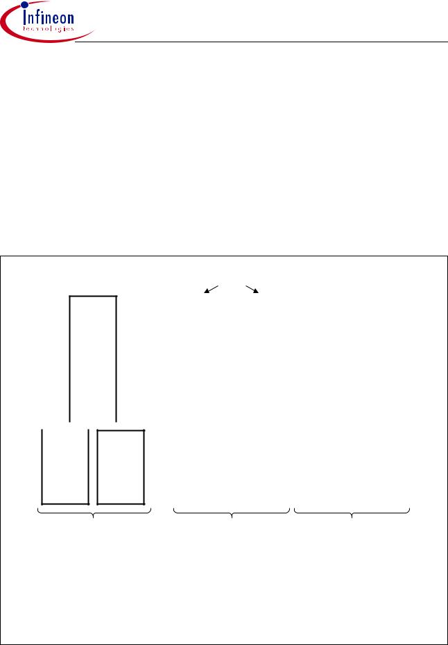
C505/C505C/C505A/C505CA
Memory Organization
The C505 CPU manipulates operands in the following four address spaces:
– On-chip program memory :16K byte ROM (C505(C)(A)-2R) or
32K byte ROM (C505A-4R/C505CA-4R) or
32K byte OTP (C505A-4E/C505CA-4E)
–Totally up to 64K byte internal/external program memory
–up to 64 Kbyte of external data memory
–256 bytes of internal data memory
–Internal XRAM data memory :256 byte (C505/C505C)
1K byte (C505A/C505CA)
– a 128 byte special function register area
Figure 5 illustrates the memory address spaces of the C505 versions.
Alternatively
FFFF H
Ext.
4000 H /  8000 H 3FFF H /
7FFF H
|
Int. |
|
|
Ext. |
||
|
|
|
|
|
|
|
(EA = |
1) |
(EA = 0) |
||||
0000H
"Code Space"
"Data Space" F700H to FFFFH:
|
|
|
|
|
|
FFFFH |
|
|
|
|||
|
|
|
|
Internal |
|
|
|
|||||
|
|
|
|
|
|
|
|
|
|
|
||
|
|
|
|
XRAM |
See table below |
|
|
|
||||
Ext. |
|
|
|
|
|
|
|
|||||
|
|
Unused |
for detailed |
|
|
|
||||||
Data |
|
|
Area |
Data Memory |
|
|
|
|||||
Memory |
|
|
|
|
partitioning |
|
|
|
||||
|
|
Int. CAN |
|
|
|
|||||||
|
|
|
|
|
|
|
||||||
|
|
|
|
|
|
|
|
|
|
|
||
|
|
|
|
Contr. |
|
|
|
|
|
|
|
|
|
|
|
|
(256 Byte) |
F700 H |
|
|
|
||||
|
|
|
|
|
|
|
|
|
||||
|
|
|
|
|
F6FF H |
|
Direct |
|||||
|
|
|
|
|
|
Indirect |
|
|||||
|
|
|
|
|
|
|
||||||
|
|
|
|
|
|
|
|
|||||
|
|
|
|
|
|
|
Addr. |
|
Addr. |
|||
|
|
|
|
|
|
|
|
|
FF H |
|
|
FF H |
|
|
Ext. |
|
|
Internal |
|
Special |
|||||
|
|
|
|
|
|
|
||||||
|
|
|
|
|
Function |
|
||||||
|
|
|
|
RAM |
|
|
||||||
|
|
Data |
|
|
|
|
||||||
|
|
|
|
|
|
Regs. |
|
|||||
|
|
|
|
|
|
|
|
|
||||
|
|
Memory |
|
|
|
|
80 H |
|
|
80 H |
||
|
|
|
|
|
|
|
|
|||||
|
|
|
|
|
|
|
|
|
|
|
7F H |
|
|
|
|
|
|
|
|
|
|
Internal |
|
||
|
|
|
|
|
|
|
|
|
|
|
|
|
|
|
|
|
|
|
|
|
|
RAM |
|
|
|
|
|
|
|
|
0000 H |
|
|
|
|
|
00 H |
|
|
|
|
|
|
|
|
|
|
|
|||
|
"Data Space" |
|
"Internal Data Space" |
|||||||||
|
|
|
|
|
|
|
|
|
|
|
MCB03632 |
|
Device |
CAN Area |
Unused Area |
XRAM Area |
||||||
|
|
|
|
|
|
|
|
|
|
C505 |
|
|
|
F700H |
|
FEFFH |
FF00H |
|
FFFFH |
|
|
|
|
|
|||||
C505C |
F700H |
|
F7FFH |
F800H |
|
FEFFH |
FF00H |
|
FFFFH |
|
|
|
|||||||
C505A |
|
|
|
F700H |
|
FBFFH |
FC00H |
|
FFFFH |
|
|
|
|
|
|||||
C505CA |
F700H |
|
F7FFH |
F800H |
|
FBFFH |
FC00H |
|
FFFFH |
|
|
|
|||||||
Figure 5
C505 Memory Map Memory Map
Data Sheet |
13 |
12.00 |
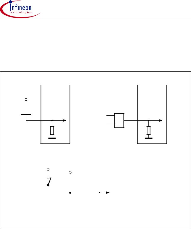
C505/C505C/C505A/C505CA
Reset and System Clock
The reset input is an active high input at pin RESET. Since the reset is synchronized internally, the RESET pin must be held high for at least two machine cycles (12 oscillator periods) while the oscillator is running. A pulldown resistor is internally connected to VSS to allow a power-up reset with an external capacitor only. An automatic reset can be obtained when VDD is applied by connecting the RESET pin to VDD via a capacitor. Figure 6 shows the possible reset circuitries.
|
|
|
a) |
b) |
||
|
|
|
|
|
|
|
VDD |
|
C505 |
|
C505 |
||
|
C505C |
|
C505C |
|||
|
|
|
|
C505A |
|
C505A |
|
|
|
|
|||
|
+ |
|
C505CA |
|
C505CA |
|
|
|
|
|
|
||
|
|
|
|
|
|
|
RESET |
RESET |
|
& |
|
|
|
|
|
|
|
c) |
|||||||
|
|
|
|
|
|
|
|
|
|
|
|
|
|
|
VDD |
|
|
VDD |
|
|
C505 |
||||||||
|
|
|
|
|
C505C |
|||||||||
|
|
|
|
|
|
|
|
C505A |
||||||
|
|
|
|
|
|
|
||||||||
|
|
|
|
+ |
|
C505CA |
||||||||
|
|
|||||||||||||
|
|
|
|
|
|
|
|
RESET |
||||||
|
|
|
|
|
|
|
|
|||||||
|
|
|
|
|
|
|
|
|
|
|
|
|
|
|
|
|
|
|
|
|
|
|
|
|
|
|
|
|
|
|
|
|
|
|
|
|
|
|
|
|
|
|
|
|
|
|
|
|
|
|
|
|
|
|
|
|
|
|
|
|
|
|
|
|
|
|
|
|
|
|
|
|
|
|
Figure 6
Reset Circuitries
Data Sheet |
14 |
12.00 |
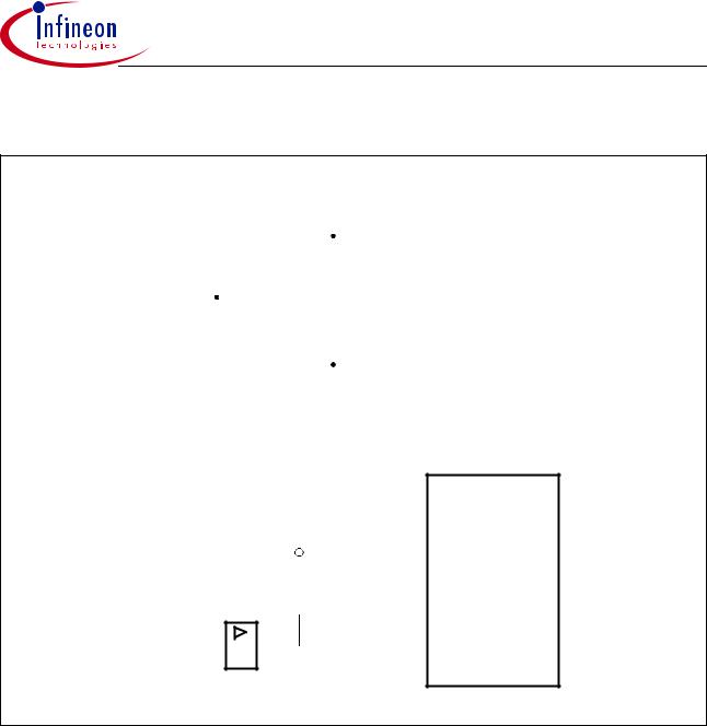
C505/C505C/C505A/C505CA
Figure 7 shows the recommended oscillator circuits for crystal and external clock operation.
|
|
C |
XTAL2 |
|||||
|
|
|
|
|
|
|
|
|
|
|
|
|
|
|
|
|
|
|
|
|
|
|
|
|
|
C505 |
|
|
|
|
|
|
|
|
|
|
2-20 |
|
|
|
C505C |
|||
|
|
|
|
|||||
|
|
|
|
|||||
|
MHz |
|
|
|
C505A |
|||
|
|
|
|
|||||
|
|
C |
|
|
C505CA |
|||
|
|
|
|
|
||||
|
|
|
|
|
|
|
|
XTAL1 |
|
|
|
|
|
|
|
|
|
|
|
|
|
|
|
|
|
|
|
|
|
|
|
|
|
|
|
|
|
|
|
|
|
|
|
|
C = 20pF ± 10pF for crystal operation
C = 20 pF ± 10pF for crystal operation
|
|
|
N.C. |
|
XTAL2 |
|
|
|
|
||
VDD |
|
C505 |
|||
|
|
|
|
|
C505C |
|
|
|
|
||
|
|
|
|
|
C505A |
|
|
|
|
||
|
|
|
|
|
C505CA |
|
|
|
|
|
|
External
Clock 


 XTAL1
XTAL1
Signal
Figure 7
Recommended Oscillator Circuitries
Data Sheet |
15 |
12.00 |
C505/C505C/C505A/C505CA
Multiple Datapointers
As a functional enhancement to the standard 8051 architecture, the C505 contains eight 16-bit datapointers instead of only one datapointer. The instruction set uses just one of these datapointers at a time. The selection of the actual datapointer is done in the special function regsiter DPSEL. Figure 8 illustrates the datapointer addressing mechanism.
- |
- |
- |
- |
- |
.2 |
.1 |
|
.0 |
|
|
|
|
|
|
|
|
|
|
|
|
|
|
|
|
|
|
|
DPSEL(92 H) |
|
|
|
|
|
|
|
DPTR7 |
|||||
|
|
|
|
|
|
|
|||||||
DPSEL |
|
|
Selected |
|
|
|
|
||||||
|
|
|
|
|
|
||||||||
|
|
|
|
|
|
||||||||
|
|
|
|
|
Data- |
|
|
|
|
|
|
||
|
|
|
|
|
|
|
|
|
|
|
|||
.2 |
|
.1 |
.0 |
|
pointer |
|
|
|
|
|
|
||
|
|
|
|
|
|
|
|
||||||
0 |
|
0 |
0 |
|
DPTR 0 |
|
|
|
|
DPTR0 |
|
||
|
|
|
|
|
|
|
|||||||
|
|
|
|
|
|
|
|||||||
|
|
|
|
|
|
|
|||||||
|
|
|
|
|
|
|
|||||||
0 |
|
0 |
1 |
|
DPTR 1 |
|
|
|
|
|
|||
|
|
|
|
DPH(83H) |
DPL(82H) |
|
|||||||
0 |
|
1 |
0 |
|
DPTR 2 |
|
|
|
|||||
0 |
|
1 |
1 |
|
DPTR 3 |
|
|
|
|
|
|
||
1 |
|
0 |
0 |
|
DPTR 4 |
|
|
|
|
|
External Data Memory |
||
1 |
|
0 |
1 |
|
DPTR 5 |
|
|
|
|
|
|||
|
|
|
|
|
|
|
|
||||||
1 |
|
1 |
0 |
|
DPTR 6 |
|
|
|
|
|
MCD00779 |
||
|
|
|
|
|
|
|
|
||||||
1 |
|
1 |
1 |
|
DPTR 7 |
|
|
|
|
|
|
||
Figure 8
External Data Memory Addressing using Multiple Datapointers
Data Sheet |
16 |
12.00 |
C505/C505C/C505A/C505CA
Enhanced Hooks Emulation Concept
The Enhanced Hooks Emulation Concept of the C500 microcontroller family is a new, innovative way to control the execution of C500 MCUs and to gain extensive information on the internal operation of the controllers. Emulation of on-chip ROM based programs is possible, too.
Each production chip has built-in logic for the supprt of the Enhanced Hooks Emulation Concept. Therefore, no costly bond-out chips are necessary for emulation. This also ensure that emulation and production chips are identical.
The Enhanced Hooks TechnologyTM 1), which requires embedded logic in the C500 allows the C500 together with an EH-IC to function similar to a bond-out chip. This simplifies the design and reduces costs of an ICE-system. ICE-systems using an EH-IC and a compatible C500 are able to emulate all operating modes of the different versions of the C500 microcontrollers. This includes emulation of ROM, ROM with code rollover and ROMless modes of operation. It is also able to operate in single step mode and to read the SFRs after a break.
|
|
|
|
ICE-System Interface |
||
|
|
|
to Emulation Hardware |
|||
SYSCON |
|
RESET |
RSYSCON |
|
|
|
|
EA |
|
|
|||
PCON |
|
RPCON |
|
EH-IC |
||
TCON |
|
ALE |
RTCON |
|
|
|
|
PSEN |
|
|
|
||
|
|
|
|
|
|
|
|
C500 |
Port 0 |
Enhanced Hooks |
|||
|
MCU |
|
Interface Circuit |
|||
|
|
Port 2 |
|
|
|
|
Optional |
Port 3 |
Port 1 |
RPort 2 |
RPort 0 |
TEA |
TALE TPSEN |
I/O Ports |
||||||
|
|
|
Target System Interface |
|
|
MCS02647 |
Figure 9
Basic C500 MCU Enhanced Hooks Concept Configuration
Port 0, port 2 and some of the control lines of the C500 based MCU are used by Enhanced Hooks Emulation Concept to control the operation of the device during emulation and to transfer informations about the programm execution and data transfer between the external emulation hardware (ICE-system) and the C500 MCU.
1)“Enhanced Hooks Technology“is a trademark and patent of Metalink Corporation licensed to Infineon Technologies.
Data Sheet |
17 |
12.00 |

C505/C505C/C505A/C505CA
Special Function Registers
The registers, except the program counter and the four general purpose register banks, reside in the special function register area. The special function register area consists of two portions : the standard special function register area and the mapped special function register area. Five special function register of the C505 (PCON1,P1ANA, VR0, VR1, VR2) are located in the mapped special function register area. For accessing the mapped special function register area, bit RMAP in special function register SYSCON must be set. All other special function registers are located in the standard special function register area which is accessed when RMAP is cleared (“0“).
The registers and data locations of the CAN controller (CAN-SFRs) are located in the external data memory area at addresses F700H to F7FFH..
Special Function Register SYSCON (Address B1H) |
|
|
Reset Value : XX100X01B |
|||||||||
(C505CA only) |
|
|
|
|
|
|
|
Reset Value : XX100001B |
||||
Bit No. |
MSB |
|
|
|
|
|
|
|
|
LSB |
||
|
|
7 |
6 |
5 |
4 |
3 |
2 |
1 |
0 |
|
||
B1H |
|
– |
– |
EALE |
RMAP |
CMOD |
CSWO |
XMAP1 |
|
XMAP0 |
SYSCON |
|
|
1) |
|
||||||||||
The functions of the shaded bits are not described here. 1) This bit is only available in the C505CA.
Bit |
Function |
|
|
|
|
RMAP |
Special function register map bit |
|
|
RMAP = 0 : The access to the non-mapped (standard) special function register |
|
|
|
area is enabled. |
|
RMAP = 1 : The access to the mapped special function register area is enabled. |
|
|
|
|
CSWO |
CAN Controller switch-off bit |
|
|
CSWO = 0 |
: CAN Controller is enabled (default after reset). |
|
CSWO = 1 |
: CAN Controller is switched off. |
|
|
|
As long as bit RMAP is set, mapped special function register area can be accessed. This bit is not cleared by hardware automatically. Thus, when non-mapped/mapped registers are to be accessed, the bit RMAP must be cleared/set respectively by software.
All SFRs with addresses where address bits 0-2 are 0 (e.g. 80H, 88H, 90H, 98H, ..., F8H, FFH) are bitaddressable.
The 52 special function registers (SFRs) in the standard and mapped SFR area include pointers and registers that provide an interface between the CPU and the other on-chip peripherals. The SFRs of the C505 are listed in Table 3 and Table 4. In Table 3 they are organized in groups which refer to the functional blocks of the C505. The CAN-SFRs (applicable for the C505C and C505CA only) are also included in Table 3. Table 4 illustrates the contents of the SFRs in numeric order of their addresses. Table 5 list the CAN-SFRs in numeric order of their addresses.
Data Sheet |
18 |
12.00 |

C505/C505C/C505A/C505CA
Table 3
Special Function Registers - Functional Blocks
Block |
Symbol |
Name |
Address |
Contents after |
||||||
|
|
|
|
Reset |
|
|
|
|
||
|
|
|
|
|
|
|
|
|
||
CPU |
ACC |
Accumulator |
E0H 1) |
00H |
|
|
|
|
||
|
B |
B-Register |
F0H 1) |
00H |
|
|
|
|
||
|
DPH |
Data Pointer, High Byte |
83H |
00H |
|
|
|
|
||
|
DPL |
Data Pointer, Low Byte |
82H |
00H |
|
|
|
|
||
|
DPSEL |
Data Pointer Select Register |
92 |
XXXXX000 |
B |
3) |
||||
|
|
|
H |
|
|
|
|
|
||
|
PSW |
Program Status Word Register |
D0H 1) |
00H |
|
|
|
|
||
|
SP |
Stack Pointer |
81H |
07H |
|
|
|
|
||
|
SYSCON2) |
System Control Register |
B1H |
XX100X01B 3) 6) |
||||||
|
|
|
FC |
XX100001B 3) 7) |
||||||
|
VR0 4) |
Version Register 0 |
C5 |
H |
|
|
|
|
||
|
|
|
H |
|
|
|
|
|
|
|
|
VR1 4) |
Version Register 1 |
FD |
05 |
H |
|
|
|
|
|
|
|
|
H |
|
|
|
|
|
||
|
VR2 4) |
Version Register 2 |
FEH |
5) |
|
|
|
|
|
|
A/D- |
ADCON0 2) |
A/D Converter Control Register 0 |
D8H 1) |
00X00000B 3) |
||||||
Converter |
ADCON1 |
A/D Converter Control Register 1 |
DC |
01XXX000 |
B |
3) |
||||
|
|
A/D Converter Data Reg. (C505/C505C) |
H |
00H |
|
|
||||
|
ADDAT |
D9H |
|
|
|
|
||||
|
ADST |
A/D Converter Start Reg. (C505/C505C) |
DAH |
XXH 3) |
|
|
|
|
||
|
ADDATH |
A/D Converter High Byte Data Register |
D9H |
00H |
|
|
|
|
||
|
|
(C505A/C505CA) |
|
|
|
|
|
|
|
|
|
ADDATL |
A/D Converter Low Byte Data Register |
DAH |
00XXXXXXB 3) |
||||||
|
|
(C505A/C505CA) |
|
|
|
|
|
|
|
|
|
P1ANA 2) 4) |
Port 1 Analog Input Selection Register |
90 |
FF |
H |
|
|
|
|
|
|
|
|
H |
|
|
|
|
|
|
|
Interrupt |
IEN0 2) |
Interrupt Enable Register 0 |
A8H 1) |
00H |
|
|
|
|
||
System |
IEN1 2) |
Interrupt Enable Register 1 |
B8H 1) |
00H |
|
|
|
|
||
|
IP0 2) |
Interrupt Priority Register 0 |
A9H |
00H |
|
|
|
|
||
|
IP1 |
Interrupt Priority Register 1 |
B9H |
XX000000B 3) |
||||||
|
TCON 2) |
Timer Control Register |
88 1) |
00 |
H |
|
|
|
|
|
|
|
|
H |
|
|
|
|
|
||
|
T2CON 2) |
Timer 2 Control Register |
C8H 1) |
00X00000B |
|
|
||||
|
SCON 2) |
Serial Channel Control Register |
98 1) |
00 |
H |
|
|
|
|
|
|
|
|
H |
|
|
|
|
|
||
|
IRCON |
Interrupt Request Control Register |
C0H 1) |
00H |
|
|
|
|
||
XRAM |
XPAGE |
Page Address Register for Extended on-chip |
91H |
00H |
|
|
|
|
||
|
|
XRAM and CAN Controller |
|
|
|
|
|
|
|
|
|
SYSCON2) |
System Control Register |
B1H |
XX100X01B 3) 6) |
||||||
|
|
|
|
XX100001B 3) 7) |
||||||
1)Bit-addressable special function registers
2)This special function register is listed repeatedly since some bits of it also belong to other functional blocks.
3)“X“means that the value is undefined and the location is reserved
4)This SFR is a mapped SFR. For accessing this SFR, bit RMAP in SFR SYSCON must be set.
5)The content of this SFR varies with the actual step of the C505 (eg. 01H for the first step)
6)C505 / C505A/C505C only
7)C505CA only
Data Sheet |
19 |
12.00 |

C505/C505C/C505A/C505CA
Table 3
Special Function Registers - Functional Blocks (cont’d)
Block |
Symbol |
Name |
Address |
Contents after |
||||||
|
|
|
|
Reset |
|
|
||||
|
|
|
|
|
|
|
|
|||
Ports |
P0 |
Port 0 |
80H 1) |
FFH |
|
|
|
|||
|
P1 |
Port 1 |
90H 1) |
FFH |
|
|
|
|||
|
P1ANA 2) 4) |
Port 1 Analog Input Selection Register |
90 1) |
FF |
H |
|
|
|
||
|
|
|
H |
|
|
|
|
|
||
|
P2 |
Port 2 |
A0H 1) |
FFH |
|
|
|
|||
|
P3 |
Port 3 |
B0H 1) |
FFH |
|
|
|
|||
|
P4 |
Port 4 |
E8H 1) |
XXXXXX11B |
|
|||||
Serial |
ADCON0 2) |
A/D Converter Control Register 0 |
D8H 1) |
00X00000B 3) |
||||||
Channel |
PCON 2) |
Power Control Register |
87 |
00 |
H |
|
|
|
||
|
SBUF |
|
H |
|
|
|
|
|||
|
Serial Channel Buffer Register |
99 |
XX |
H |
3) |
|
|
|||
|
|
|
H |
|
|
|
|
|
|
|
|
SCON |
Serial Channel Control Register |
98H 1) |
00H |
|
|
|
|||
|
SRELL |
Serial Channel Reload Register, low byte |
AAH |
D9H |
|
|
|
|||
|
SRELH |
Serial Channel Reload Register, high byte |
BAH |
XXXXXX11B 3) |
||||||
Timer 0/ |
TCON |
Timer 0/1 Control Register |
88H 1) |
00H |
|
|
|
|||
Timer 1 |
TH0 |
Timer 0, High Byte |
8CH |
00H |
|
|
|
|||
|
TH1 |
Timer 1, High Byte |
8DH |
00H |
|
|
|
|||
|
TL0 |
Timer 0, Low Byte |
8AH |
00H |
|
|
|
|||
|
TL1 |
Timer 1, Low Byte |
8BH |
00H |
|
|
|
|||
|
TMOD |
Timer Mode Register |
89H |
00H |
|
|
|
|||
Compare/ |
CCEN |
Comp./Capture Enable Reg. |
C1H |
00H 3) |
|
|
||||
Capture |
CCH1 |
Comp./Capture Reg. 1, High Byte |
C3H |
00H |
|
|
|
|||
Unit / |
CCH2 |
Comp./Capture Reg. 2, High Byte |
C5H |
00H |
|
|
|
|||
Timer 2 |
CCH3 |
Comp./Capture Reg. 3, High Byte |
C7H |
00H |
|
|
|
|||
|
CCL1 |
Comp./Capture Reg. 1, Low Byte |
C2H |
00H |
|
|
|
|||
|
CCL2 |
Comp./Capture Reg. 2, Low Byte |
C4H |
00H |
|
|
|
|||
|
CCL3 |
Comp./Capture Reg. 3, Low Byte |
C6H |
00H |
|
|
|
|||
|
CRCH |
Reload Register High Byte |
CBH |
00H |
|
|
|
|||
|
CRCL |
Reload Register Low Byte |
CAH |
00H |
|
|
|
|||
|
TH2 |
Timer 2, High Byte |
CDH |
00H |
|
|
|
|||
|
TL2 |
Timer 2, Low Byte |
CCH |
00H |
|
|
|
|||
|
T2CON |
Timer 2 Control Register |
C8H 1) |
00X00000B 3) |
||||||
|
IEN0 2) |
Interrupt Enable Register 0 |
A8H 1) |
00H |
|
|
|
|||
|
IEN1 2) |
Interrupt Enable Register 1 |
B8H 1) |
00H |
|
|
|
|||
Watchdog |
WDTREL |
Watchdog Timer Reload Register |
86H |
00H |
|
|
|
|||
|
IEN0 2) |
Interrupt Enable Register 0 |
A8H 1) |
00H |
|
|
|
|||
|
IEN1 2) |
Interrupt Enable Register 1 |
B8H 1) |
00H |
|
|
|
|||
|
IP0 2) |
Interrupt Priority Register 0 |
A9H |
00H |
|
|
|
|||
Pow. Save |
PCON 2) |
Power Control Register |
87 |
00 |
H |
|
|
|
||
|
|
|
H |
|
|
|
|
|||
Modes |
PCON1 4) |
Power Control Register 1 |
88 1) |
0XX0XXXX |
B |
3) |
||||
|
|
|
H |
|
|
|
|
|
|
|
1)Bit-addressable special function registers
2)This special function register is listed repeatedly since some bits of it also belong to other functional blocks.
3)“X“means that the value is undefined and the location is reserved
4)SFR is located in the mapped SFR area. For accessing this SFR, bit RMAP in SFR SYSCON must be set.
Data Sheet |
20 |
12.00 |

C505/C505C/C505A/C505CA
Table 3
Special Function Registers - Functional Blocks (cont’d)
Block |
Symbol |
Name |
Address |
Contents after |
||||
|
|
|
|
|
Reset |
|||
|
|
|
|
|
|
|
||
CAN |
CR |
Control Register |
F700H |
|
01H |
|
||
Controller |
SR |
Status Register |
F701 |
|
XX |
H |
3) |
|
|
IR |
Interrupt Register |
H |
|
XX |
|
||
|
F702 |
|
H |
3) |
||||
(C505C/ |
|
|
H |
|
|
|
||
BTR0 |
Bit Timing Register Low |
F704 |
|
UU |
H |
3) |
||
C505CA |
BTR1 |
Bit Timing Register High |
H |
|
|
|
|
|
F705H |
|
0UUUUUUUB 3) |
||||||
only) |
GMS0 |
Global Mask Short Register Low |
F706 |
|
UU |
H |
3) |
|
|
|
|
H |
|
|
|
|
|
|
GMS1 |
Global Mask Short Register High |
F707H |
|
UUU11111B 3) |
|||
|
UGML0 |
Upper Global Mask Long Register Low |
F708 |
|
UU |
H |
3) |
|
|
UGML1 |
Upper Global Mask Long Register High |
H |
|
UU |
|
||
|
F709 |
|
H |
3) |
||||
|
LGML0 |
|
H |
|
UU |
|
||
|
Lower Global Mask Long Register Low |
F70A |
|
H |
3) |
|||
|
|
|
H |
|
|
|
|
|
|
LGML1 |
Lower Global Mask Long Register High |
F70BH |
|
UUUUU000B 3) |
|||
|
UMLM0 |
Upper Mask of Last Message Register Low |
F70C |
|
UU |
H |
3) |
|
|
UMLM1 |
|
H |
|
UU |
|
||
|
Upper Mask of Last Message Register High |
F70D |
|
H |
3) |
|||
|
LMLM0 |
|
H |
|
UU |
|
||
|
Lower Mask of Last Message Register Low |
F70E |
|
H |
3) |
|||
|
|
|
H |
|
|
|
|
|
|
LMLM1 |
Lower Mask of Last Message Register High |
F70FH |
|
UUUUU000B 3) |
|||
|
|
Message Object Registers : |
|
|
|
|
|
|
|
MCR0 |
Message Control Register Low |
F7n0 |
5) |
UU |
H |
3) |
|
|
|
|
H |
|
|
|
|
|
|
MCR1 |
Message Control Register High |
F7n1 |
5) |
UU |
H |
3) |
|
|
|
|
H |
|
|
|
|
|
|
UAR0 |
Upper Arbitration Register Low |
F7n2 |
5) |
UU |
H |
3) |
|
|
|
|
H |
|
|
|
|
|
|
UAR1 |
Upper Arbitration Register High |
F7n3 |
5) |
UU |
H |
3) |
|
|
|
|
H |
|
|
|
|
|
|
LAR0 |
Lower Arbitration Register Low |
F7n4 |
5) |
UU |
H |
3) |
|
|
|
|
H |
|
|
|
|
|
|
LAR1 |
Lower Arbitration Register High |
F7n5H 5) |
UUUUU000B 3) |
||||
|
MCFG |
Message Configuration Register |
F7n6H 5) |
UUUUUU00B3) |
||||
|
DB0 |
Message Data Byte 0 |
F7n7 |
5) |
XX |
H |
3) |
|
|
|
|
H |
|
|
|
||
|
DB1 |
Message Data Byte 1 |
F7n8 |
5) |
XX |
H |
3) |
|
|
|
|
H |
|
|
|
||
|
DB2 |
Message Data Byte 2 |
F7n9 |
5) |
XX |
H |
3) |
|
|
|
|
H |
|
|
|
||
|
DB3 |
Message Data Byte 3 |
F7nA |
5) |
XX |
H |
3) |
|
|
|
|
H |
|
|
|
||
|
DB4 |
Message Data Byte 4 |
F7nB |
5) |
XX |
H |
3) |
|
|
|
|
H |
|
|
|
||
|
DB5 |
Message Data Byte 5 |
F7nC |
5) |
XX |
H |
3) |
|
|
|
|
H |
|
|
|
||
|
DB6 |
Message Data Byte 6 |
F7nD |
5) |
XX |
H |
3) |
|
|
|
|
H |
|
|
|
||
|
DB7 |
Message Data Byte 7 |
F7nE |
5) |
XX |
H |
3) |
|
|
|
|
H |
|
|
|
||
1)Bit-addressable special function registers
2)This special function register is listed repeatedly since some bits of it also belong to other functional blocks.
3)“X“means that the value is undefined and the location is reserved. “U“means that the value is unchanged by a reset operation. “U“values are undefined (as “X“) after a power-on reset operation
4)SFR is located in the mapped SFR area. For accessing this SFR, bit RMAP in SFR SYSCON must be set.
5)The notation “n“(n= 1 to F) in the message object address definition defines the number of the related message object.
Data Sheet |
21 |
12.00 |

C505/C505C/C505A/C505CA
Table 4
Contents of the SFRs, SFRs in numeric order of their addresses
Addr |
Register |
Content |
Bit 7 |
Bit 6 |
Bit 5 |
Bit 4 |
Bit 3 |
Bit 2 |
Bit 1 |
Bit 0 |
||||||||
|
|
|
after |
|
|
|
|
|
|
|
|
|
|
|
|
|
||
|
|
|
Reset1) |
|
|
|
|
|
|
|
|
|
|
|
|
|
||
80 |
2) |
P0 |
FF |
H |
.7 |
.6 |
|
|
.5 |
.4 |
.3 |
.2 |
|
|
.1 |
.0 |
|
|
H |
|
|
|
|
|
|
|
|
|
|
|
|
|
|
|
|
|
|
81H |
|
SP |
07H |
.7 |
.6 |
|
|
.5 |
.4 |
.3 |
.2 |
|
|
.1 |
.0 |
|
||
82H |
|
DPL |
00H |
.7 |
.6 |
|
|
.5 |
.4 |
.3 |
.2 |
|
|
.1 |
.0 |
|
||
83H |
|
DPH |
00H |
.7 |
.6 |
|
|
.5 |
.4 |
.3 |
.2 |
|
|
.1 |
.0 |
|
||
86H |
|
WDTREL |
00H |
WDT |
.6 |
|
|
.5 |
.4 |
.3 |
.2 |
|
|
.1 |
.0 |
|
||
|
|
|
|
|
|
PSEL |
|
|
|
|
|
|
|
|
|
|
|
|
|
|
|
|
|
|
|
|
|
|
|
|
|||||||
87H |
|
PCON |
00H |
SMOD |
PDS |
IDLS |
SD |
GF1 |
GF0 |
PDE |
IDLE |
|||||||
88 |
2) |
TCON |
00 |
H |
TF1 |
TR1 |
TF0 |
TR0 |
IE1 |
IT1 |
IE0 |
IT0 |
||||||
H |
|
|
|
|
|
|
|
|
|
|
|
|
|
|
|
|
||
88 |
3) |
PCON1 |
0XX0- |
EWPD |
– |
– |
WS |
– |
– |
– |
– |
|||||||
H |
|
|
XXXXB |
|
|
|
|
|
|
|
|
|
|
|
|
|
||
|
|
|
|
|
|
|
|
|
|
|
|
|
|
|
|
|||
89H |
|
TMOD |
00H |
GATE |
|
|
|
|
|
|
|
|
|
|
|
|
||
|
C/T |
|
M1 |
M0 |
GATE |
C/T |
M1 |
M0 |
||||||||||
8AH |
|
TL0 |
00H |
.7 |
.6 |
|
|
.5 |
.4 |
.3 |
.2 |
|
|
.1 |
.0 |
|
||
8BH |
|
TL1 |
00H |
.7 |
.6 |
|
|
.5 |
.4 |
.3 |
.2 |
|
|
.1 |
.0 |
|
||
8CH |
|
TH0 |
00H |
.7 |
.6 |
|
|
.5 |
.4 |
.3 |
.2 |
|
|
.1 |
.0 |
|
||
8DH |
|
TH1 |
00H |
.7 |
.6 |
|
|
.5 |
.4 |
.3 |
.2 |
|
|
.1 |
.0 |
|
||
90 |
2) |
P1 |
FF |
|
T2 |
CLK- |
T2EX |
.4 |
INT6 |
INT5 |
INT4 |
|
|
|||||
H |
.INT3 |
|||||||||||||||||
H |
|
|
|
|
|
OUT |
|
|
|
|
|
|
|
|
|
|||
|
|
|
|
|
|
|
|
|
|
|
|
|
|
|
|
|||
|
|
|
|
|
|
|
|
|
|
|
|
|
|
|||||
90 |
3) |
P1ANA |
FF |
H |
EAN7 |
EAN6 |
EAN5 |
EAN4 |
EAN3 |
EAN2 |
EAN1 |
EAN0 |
||||||
H |
|
|
|
|
|
|
|
|
|
|
|
|
|
|
|
|
|
|
91H |
|
XPAGE |
00H |
.7 |
.6 |
|
|
.5 |
.4 |
.3 |
.2 |
|
|
.1 |
.0 |
|
||
92H |
|
DPSEL |
XXXX- |
– |
– |
– |
– |
– |
.2 |
|
|
.1 |
.0 |
|
||||
|
|
|
X000B |
|
|
|
|
|
|
|
|
|
|
|
|
|
||
98 |
2) |
SCON |
00 |
H |
SM0 |
SM1 |
SM2 |
REN |
TB8 |
RB8 |
TI |
RI |
||||||
H |
|
|
|
|
|
|
|
|
|
|
|
|
|
|
|
|
||
99H |
|
SBUF |
XXH |
.7 |
.6 |
|
|
.5 |
.4 |
.3 |
.2 |
|
|
.1 |
.0 |
|
||
A0H2) |
P2 |
FFH |
.7 |
.6 |
|
|
.5 |
.4 |
.3 |
.2 |
|
|
.1 |
.0 |
|
|||
A8H2) |
IEN0 |
00H |
EA |
WDT |
ET2 |
ES |
ET1 |
EX1 |
ET0 |
EX0 |
||||||||
A9H |
|
IP0 |
00H |
OWDS |
WDTS |
.5 |
.4 |
.3 |
.2 |
|
|
.1 |
.0 |
|
||||
AAH |
SRELL |
D9H |
.7 |
.6 |
|
|
.5 |
.4 |
.3 |
.2 |
|
|
.1 |
.0 |
|
|||
1)X means that the value is undefined and the location is reserved
2)Bit-addressable special function registers
3)SFR is located in the mapped SFR area. For accessing this SFR, bit RMAP in SFR SYSCON must be set.
Data Sheet |
22 |
12.00 |

C505/C505C/C505A/C505CA
Table 4
Contents of the SFRs, SFRs in numeric order of their addresses (cont’d)
Addr |
Register |
Content |
Bit 7 |
Bit 6 |
Bit 5 |
Bit 4 |
Bit 3 |
Bit 2 |
Bit 1 |
Bit 0 |
||||
|
|
after |
|
|
|
|
|
|
|
|
|
|
|
|
|
|
Reset1) |
|
|
|
|
|
|
|
|
|
|
|
|
B0H2) |
P3 |
FFH |
|
|
|
|
T1 |
T0 |
|
|
|
|
TxD |
RxD |
RD |
WR |
INT1 |
INT0 |
|||||||||||
B1H |
SYSCON |
XX10- |
– |
– |
EALE |
RMAP |
CMOD |
– |
XMAP1 |
XMAP0 |
||||
|
3) |
0X01B |
|
|
|
|
|
|
|
|
|
|
|
|
|
|
|
|
|
|
|
|
|
|
|
|
|
|
|
B1H |
SYSCON |
XX10- |
– |
– |
EALE |
RMAP |
CMOD |
CSWO |
XMAP1 |
XMAP0 |
||||
|
4) |
0001B |
|
|
|
|
|
|
|
|
|
|
|
|
|
|
|
|
|
|
|
|
|
|
|
|
|
|
|
B8H 2) |
IEN1 |
00H |
EXEN2 |
SWDT |
EX6 |
EX5 |
EX4 |
EX3 |
ECAN |
EADC |
||||
B9H |
IP1 |
XX00- |
– |
– |
.5 |
.4 |
.3 |
|
.2 |
|
.1 |
.0 |
||
|
|
0000B |
|
|
|
|
|
|
|
|
|
|
|
|
BAH |
SRELH |
XXXX- |
– |
– |
– |
– |
– |
– |
.1 |
.0 |
||||
|
|
XX11B |
|
|
|
|
|
|
|
|
|
|
|
|
C0H2) |
IRCON |
00H |
EXF2 |
TF2 |
IEX6 |
IEX5 |
IEX4 |
IEX3 |
SWI |
IADC |
||||
C1H |
CCEN |
00H |
COCA |
COCAL |
COCA |
COCAL |
COCA |
COCAL |
COCA |
COCAL |
||||
|
|
|
H3 |
3 |
|
H2 |
2 |
H1 |
1 |
|
H0 |
0 |
||
|
|
|
|
|
|
|
|
|
|
|
|
|
|
|
C2H |
CCL1 |
00H |
.7 |
|
.6 |
|
.5 |
.4 |
.3 |
|
.2 |
|
.1 |
.0 |
C3H |
CCH1 |
00H |
.7 |
|
.6 |
|
.5 |
.4 |
.3 |
|
.2 |
|
.1 |
.0 |
C4H |
CCL2 |
00H |
.7 |
|
.6 |
|
.5 |
.4 |
.3 |
|
.2 |
|
.1 |
.0 |
C5H |
CCH2 |
00H |
.7 |
|
.6 |
|
.5 |
.4 |
.3 |
|
.2 |
|
.1 |
.0 |
C6H |
CCL3 |
00H |
.7 |
|
.6 |
|
.5 |
.4 |
.3 |
|
.2 |
|
.1 |
.0 |
C7H |
CCH3 |
00H |
.7 |
|
.6 |
|
.5 |
.4 |
.3 |
|
.2 |
|
.1 |
.0 |
C8H2) |
T2CON |
00X0- |
T2PS |
I3FR |
– |
T2R1 |
T2R0 |
T2CM |
T2I1 |
T2I0 |
||||
|
|
0000B |
|
|
|
|
|
|
|
|
|
|
|
|
CAH |
CRCL |
00H |
.7 |
|
.6 |
|
.5 |
.4 |
.3 |
|
.2 |
|
.1 |
.0 |
CBH |
CRCH |
00H |
.7 |
|
.6 |
|
.5 |
.4 |
.3 |
|
.2 |
|
.1 |
.0 |
CCH |
TL2 |
00H |
.7 |
|
.6 |
|
.5 |
.4 |
.3 |
|
.2 |
|
.1 |
.0 |
CDH |
TH2 |
00H |
.7 |
|
.6 |
|
.5 |
.4 |
.3 |
|
.2 |
|
.1 |
.0 |
D0H2) |
PSW |
00H |
CY |
AC |
F0 |
RS1 |
RS0 |
OV |
F1 |
P |
||||
D8H2) |
ADCON0 |
00X0- |
BD |
CLK |
– |
BSY |
ADM |
MX2 |
MX1 |
MX0 |
||||
|
|
0000B |
|
|
|
|
|
|
|
|
|
|
|
|
1)X means that the value is undefined and the location is reserved
2)Bit-addressable special function registers
3)C505 /C505C/C505A only
4)C505CA only
Data Sheet |
23 |
12.00 |
 Loading...