


ICST AV9155C-36CN20, AV9155C-36CM20, AV9155C-23CN20, AV9155C-23CM20, AV9155C-02CN20 Datasheet
...
Integrated |
AV9155C |
Circuit
Systems, Inc.
Low Cost 20-Pin Frequency Generator
General Description
The AV9155C is a low cost frequency generator designed specifically for desktop and notebook PC applications with either 3.3V or 5.0V power supply voltage. Its CPU clocks provide all necessary CPU frequencies for 286, 386 and 486 systems, including support for the latest speeds of processors. The device uses a 14.318 MHz crystal to generate the CPU and all peripheral clocks for integrated desktop motherboards.
The dual 14.318 MHz clock outputs allows one output for the system and one to be the input to an ICS graphics frequency generator such as the AV9194.
The CPU clock offers the unique feature of smooth, glitchfree transitions from one frequency to the next, making this ideal device to use whenever slowing the CPU speed. The AV9155C makes a gradual transition between frequencies, so that it obeys the Intel cycle-to-cycle timing specification for 486 systems. The simultaneous 2X and 1X CPU clocks offer controlled skew to within 1.5ns (max) of each other.
ICS offers several versions of the AV9155C. The different devices are shown below:
Features
•Compatible with 286, 386, and 486 CPUs
•Supports turbo modes
•Generates communications clock, keyboard clock, floppy disk clock, system reference clock, bus clock and CPU clock
•Output enable tristates outputs
•Up to 100 MHz at 5V or 3.3V
•20-pin DIP or SOIC
•All loop filter components internal
•Skew-controlled 2X and 1X CPU clocks
•Power-down option
ICS has been shipping motherboard frequency generators since April 1990, and is the leader in the area of multiple output clocks on a single chip. The AV9155C is a third generation device, and uses ICS’s patented analog CMOS phase-locked loop technology for low phase jitter. ICS offers a broad family of frequency generators for motherboards, graphics and other applications, including cost-effective versions with only one or two output clocks. Consult ICS for all of your clock generation needs.
PART |
DESCRIPTION |
|
|
AV9155C-01 |
Motherboard clock generator with 16 MHz BUS CLK |
|
|
AV9155C-02 |
Motherboard clock generator with 32 MHz BUS CLK |
|
|
AV9155C-23 |
Includes PentiumÔ frequencies |
|
|
AV9155C-36 |
Features a special 40 MHz SCSI clock |
|
|
Block Diagram
Pentium is a trademark of Intel Corporation.
AV9155C Rev F 12/13/00
AV9155C
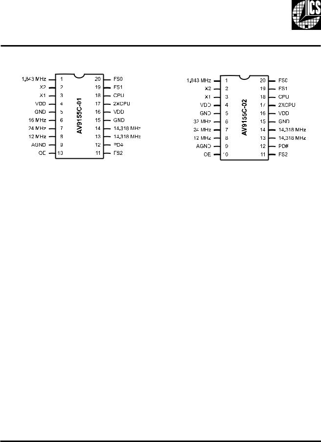
Pin Configuration
20-Pin DIP or SOIC |
20-Pin DIP or SOIC |
Pin Descriptions for AV9155C-01, -02
PIN |
PIN NAME |
TYPE |
DESCRIPTION |
|
NUMBER |
||||
|
|
|
||
|
|
|
|
|
1 |
1.843 MHz |
Output |
1.84 MHz clock output. |
|
|
|
|
|
|
2 |
X2 |
Output |
Crystal connection. |
|
|
|
|
|
|
3 |
X1 |
Input |
Crystal connection. |
|
|
|
|
|
|
4 |
VDD |
- |
Digital power supply (3.3V or 5.0V). |
|
|
|
|
|
|
5 |
GND |
- |
Digital Ground. |
|
|
|
|
|
|
6 |
16 MHz/32 MHz |
Output |
16 MHz (-01) or 32 MHz (-02) clock output. |
|
|
|
|
|
|
7 |
24 MHz |
Output |
24 MHz floppy disk/combination I/O clock output. |
|
|
|
|
|
|
8 |
12 MHz |
Output |
12 MHz keyboard clock output. |
|
|
|
|
|
|
9 |
AGND |
- |
Analog ground (original version). |
|
|
|
|
|
|
10 |
OE |
Input |
Output enable. Tristates all outputs when low. (Has internal pull-up.) |
|
11 |
FS2 |
Input |
CPU clock frequency select #2. (Has internal pull-up.) |
|
|
|
|
|
|
12 |
PD# |
Input |
Power-down. Shuts off entire chip when low. (Has internal pull-up.) |
|
|
|
|
|
|
13 |
14.318 MHz |
Output |
14.318 MHz reference clock output. |
|
|
|
|
|
|
14 |
14.318 MHz |
Output |
14.318 MHz reference clock output. |
|
|
|
|
|
|
15 |
GND |
- |
Digital ground. |
|
|
|
|
|
|
16 |
VDD |
- |
Digital power supply (3.3V or 5.0V). |
|
|
|
|
|
|
17 |
2XCPU |
Output |
2X CPU clock output. |
|
|
|
|
|
|
18 |
CPU |
Output |
1X CPU clock output. |
|
|
|
|
|
|
19 |
FS1 |
Input |
CPU clock frequency select #1. (Has internal pull-up.) |
|
|
|
|
|
|
20 |
FS0 |
Input |
CPU clock frequency select #0. (Has internal pull-up.) |
|
|
|
|
|
2

AV9155C
Functionality - AV9155C-01
(Using 14.318 MHz input.All frequencies in MHz.)
CLOCK#2CPUand2XCPU
FS2 |
FS1 |
FS0 |
2XCPU |
CPU |
(Pin 11) |
(Pin 19) |
(Pin 20) |
(Pin 17) |
(Pin 18) |
|
|
|
|
|
0 |
0 |
0 |
8 |
4 |
0 |
0 |
1 |
16 |
8 |
0 |
1 |
0 |
32 |
16 |
0 |
1 |
1 |
40 |
20 |
1 |
0 |
0 |
50 |
25 |
1 |
0 |
1 |
66.66 |
33.33 |
1 |
1 |
0 |
80* |
40* |
1 |
1 |
1 |
100* |
50* |
|
|
|
|
|
*VDD minimum 3.15V.
PERIPHERAL CLOCKS
COMMCLK |
BUSCLK |
FDCLK |
KBCLK |
(Pin 1) |
(Pin 6) |
(Pin 7) |
(Pin 8) |
|
|
|
|
1.843 |
16 |
24 |
12 |
|
|
|
|
REFERENCE CLOCKS
REFCLK1 |
REFCLK2 |
(Pin 13) |
(Pin 14) |
|
|
14.318 |
14.318 |
|
|
Functionality - AV9155C-02
(Using 14.318 MHz input.All frequencies in MHz.)
CLOCK#2CPUand2XCPU
FS2 |
FS1 |
FS0 |
2XCPU |
CPU |
(Pin 11) |
(Pin 19) |
(Pin 20) |
(Pin 17) |
(Pin 18) |
|
|
|
|
|
0 |
0 |
0 |
8 |
4 |
0 |
0 |
1 |
16 |
8 |
0 |
1 |
0 |
32 |
16 |
0 |
1 |
1 |
40 |
20 |
1 |
0 |
0 |
50 |
25 |
1 |
0 |
1 |
66.66 |
33.33 |
1 |
1 |
0 |
80* |
40* |
1 |
1 |
1 |
100* |
50* |
|
|
|
|
|
* VDD minimum 3.15V
PERIPHERAL CLOCKS
COMMCLK |
BUSCLK |
FDCLK |
KBCLK |
(Pin 1) |
(Pin 6) |
(Pin 7) |
(Pin 8) |
|
|
|
|
1.843 |
32 |
24 |
12 |
|
|
|
|
REFERENCE CLOCKS
REFCLK1 |
REFCLK2 |
(Pin 13) |
(Pin 14) |
|
|
14.318 |
14.318 |
|
|
Frequency Transitions |
Using an Input Clock as Reference |
A key feature of the AV9155C is its ability to provide smooth, glitch-free frequency transitions on the CPU and 2XCPU clocks when the frequency select pins are changed. These frequency transitions do not violate the Intel 486 specification of less than 0.1% frequency change per clock period.
The AV9155C is designed to accept a 14.318 MHz crystal as the input reference. With some external changes, it is possible to use a crystal oscillator or clock input. Please see application note AN04 for details on driving the AV9155C with a clock.
3
AV9155C
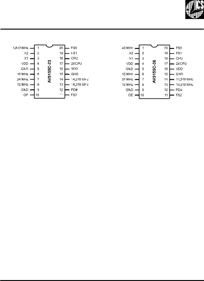
Pin Configuration
20-Pin DIP or SOIC |
20-Pin DIP or SOIC |
Pin Descriptions for AV9155C-23, -36
PIN |
PIN |
TYPE |
DESCRIPTION |
|
NUMBER |
NAME |
|||
|
|
|||
|
|
|
|
|
1 |
1.843/40 MHz |
Output |
1.84 MHz (-23)/40 MHz SCSI (-36) clock output. |
|
|
|
|
|
|
2 |
X2 |
Output |
Crystal connection. |
|
|
|
|
|
|
3 |
X1 |
Input |
Crystal connection. |
|
|
|
|
|
|
4 |
VDD |
- |
Digital power supply (3.3V or 5.0V). |
|
|
|
|
|
|
5 |
GND |
- |
Digital ground. |
|
|
|
|
|
|
6 |
16 MHz/15 MHz |
Output |
16 MHz (-23)/15 MHz (-36) clock output. |
|
|
|
|
|
|
7 |
24 MHz |
Output |
24 MHz floppy disk/combination I/O clock output. |
|
|
|
|
|
|
8 |
12 MHz |
Output |
12 MHz keyboard clock output. |
|
|
|
|
|
|
9 |
AGND |
- |
Analog ground (original version). |
|
|
|
|
|
|
10 |
OE |
Input |
Output enable. Tristates all outputs when low. (Has internal pull-up.) |
|
|
|
|
|
|
11 |
FS2 |
Input |
CPU clock frequency select #2. (-23 has internal pull-up.) |
|
|
|
|
|
|
12 |
PD# |
Input |
Power-down. Shuts off entire chip when low. (Has internal pull-up.) |
|
|
|
|
|
|
13 |
14.318 MHz |
Output |
14.318 MHz reference clock output. |
|
|
|
|
|
|
14 |
14.318 MHz |
Output |
14.318 MHz reference clock output. |
|
|
|
|
|
|
15 |
GND |
- |
Digital ground. |
|
|
|
|
|
|
16 |
VDD |
- |
Digital power supply (3.3V or 5.0V). |
|
|
|
|
|
|
17 |
2XCPU |
Output |
2X CPU clock output. |
|
|
|
|
|
|
18 |
CPU |
Output |
1X CPU clock output. |
|
|
|
|
|
|
19 |
FS1 |
Input |
CPU clock frequency select #1. (-23 has internal pull-up.) |
|
|
|
|
|
|
20 |
FS0 |
Input |
CPU clock frequency select #0. (-23 has internal pull-up.) |
4

AV9155C
Functionality - AV9155C-23
(Using 14.318 MHz input.All frequencies in MHz.)
CLOCK#2CPUand2XCPU
FS2 |
FS1 |
FS0 |
2XCPU |
CPU |
(Pin 11) |
(Pin 19) |
(Pin 20) |
(Pin 17) |
(Pin 18) |
|
|
|
|
|
0 |
0 |
0 |
75* |
37.5* |
0 |
0 |
1 |
32 |
16 |
0 |
1 |
0 |
60 |
30 |
0 |
1 |
1 |
40 |
20 |
1 |
0 |
0 |
50 |
25 |
1 |
0 |
1 |
66.66 |
33.33 |
1 |
1 |
0 |
80* |
40* |
1 |
1 |
1 |
52 |
26 |
|
|
|
|
|
*VDDminimum3.15V
Functionality - AV9155C-36
(Using 14.318 MHz input.All frequencies in MHz.)
CLOCK#2CPUand2XCPU
FS2 |
FS1 |
FS0 |
2XCPU |
CPU |
(Pin 11) |
(Pin 19) |
(Pin 20) |
(Pin 17) |
(Pin 18) |
|
|
|
|
|
0 |
0 |
0 |
8 |
4 |
0 |
0 |
1 |
16 |
8 |
0 |
1 |
0 |
60 |
30 |
0 |
1 |
1 |
40 |
20 |
1 |
0 |
0 |
50 |
25 |
1 |
0 |
1 |
66.66 |
33.33 |
1 |
1 |
0 |
80* |
40* |
1 |
1 |
1 |
100* |
50* |
*VDDminimum3.15V
PERIPHERAL CLOCKS
COMMCLK |
BUSCLK (Pin |
FDCLK |
KBCLK |
(Pin 1) |
6) |
(Pin 7) |
(Pin 8) |
|
|
|
|
1.843 |
16 |
24 |
12 |
|
|
|
|
REFERENCE CLOCKS
REFCLK1 |
REFCLK2 |
(Pin 13) |
(Pin 14) |
|
|
14.318 |
14.318 |
|
|
PERIPHERAL CLOCKS
SCSICLK |
BUSCLK (Pin |
FDCLK |
KBCLK |
(Pin 1) |
6) |
(Pin 7) |
(Pin 8) |
|
|
|
|
40 |
15 |
24 |
12 |
|
|
|
|
REFERENCE CLOCKS
REFCLK1 |
REFCLK2 |
(Pin 13) |
(Pin 14) |
|
|
14.318 |
14.318 |
|
|
5
 Loading...