


ICSI IC62LV5128L-55HI, IC62LV5128L-55T, IC62LV5128L-55TI, IC62LV5128L-70B, IC62LV5128L-70BI Datasheet
...IC62LV5128L
IC62LV5128LL
Document Title
512Kx8 bit Low Voltage and Ultra Low Power CMOS Static RAM
Revision History
Revision No |
History |
Draft Date |
Remark |
|
0A |
Initial Draft |
May 1,2001 |
Preliminary |
|
0B |
1. |
Change for tPWE: 45 to 40 ns for 55 ns product |
August 31,2001 |
|
|
|
: 60 to 40 ns for 70 ns product |
|
|
|
2. |
Change for VCC: 2.2-3.6V to 2.7-3.6V |
|
|
3.1Change for ICC test conditiomn: VCC=Max. to 3V
3.2Change for ICC: 30 to 25mA for 55 ns product
25 to 20mA for 70 ns porduct
20 to 15 mA for 100 ns product
4.1Change for VDR Min. : 1.2 to 1.5V
4.2Change for IDR test condition: VCC=1.2 to 1.5V and IDR 5. Change for tHZCE 25 to 20 ns for 55 ns product
6. Change for tHZWE 33 to 30 ns for 70 ns product
The attached datasheets are provided by ICSI. Integrated Circuit Solution Inc reserve the right to change the specifications and products. ICSI will answer to your questions about device. If you have any questions, please contact the ICSI offices.
Integrated Circuit Solution Inc. |
1 |
LPSR012-0B 08/31/2001
IC62LV5128L
IC62LV5128LL
512K x 8 LOW POWER and LOW VCC CMOS STATIC RAM
FEATURES
•Access times of 55, 70, 100 ns
•CMOS Low power operation:
—60 mW (typical) operation
—3 µW (typical) standby
•Low data retention voltage: 1.5V (min.)
•Output Enable (OE) and Chip Enable (CE) inputs for ease in applications
•TTL compatible inputs and outputs
•Fully static operation:
—No clock or refresh reguired
•Single 2.7V-3.6V power supply
•Available in the 32-pin 8*20mm TSOP-1, 32-pin 8*13.4mm TSOP-1 and 48-pin 6*8mm TF-BGA
DESCRIPTION
The ICSI IC62LV5128L and IC62LV5128LL is a low voltage, 524,288 words by 8 bits, CMOS SRAM. It is fabricated using ICSI's low voltage, six transistor (6T), CMOS technology. The device is targeted to satisfy the demands of the state-of-the-art technologies such as cell phones and pagers.
When CE is HIGH (deselected), the device assumes a standby mode at which the power dissipation can be reduced down with CMOS input levels. Additionally, easy memory expansion is provided by using Chip Enable and Output Enable inputs, CE and OE. The active LOW Write Enable ( WE) controls both writing and reading of the memory.
The IC62LV5128L and IC62LV5128LL are available in 32-pin 8*20mm TSOP-1, 8*13.4mm TSOP-1 and 48-pin 6*8mm TFBGA.
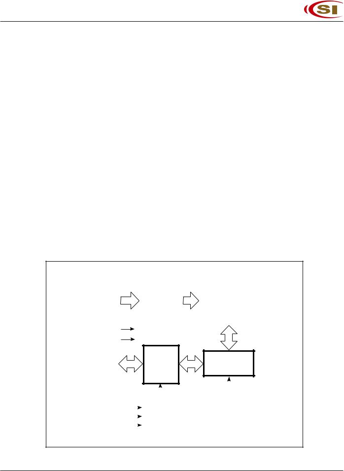
FUNCTIONAL BLOCK DIAGRAM
A0-A18 |
DECODER |
|
512K x 8 |
|
MEMORY ARRAY |
||
|
|
|
|
|
|
|
|
VCC
GND
I/O
I/O0-I/O7 DATA COLUMN I/O
CIRCUIT
|
|
|
|
|
|
|
|
|
|
|
|
|
|
|
|
|
|
|
|
|
|
|
|
|
|
|
CE |
|
|
CONTROL |
|
||||
|
|
|||||||
|
|
|
|
|
|
|
||
OE |
|
|
|
|||||
|
|
CIRCUIT |
|
|||||
|
|
|
|
|
|
|
||
WE |
|
|
|
|
|
|||
|
|
|
|
|||||
|
|
|
|
|
|
|
|
|
ICSI reserves the right to make changes to its products at any time without notice in order to improve design and supply the best possible product. We assume no responsibility for any errors which may appear in this publication. © Copyright 2000, Integrated Circuit Solution Inc.
2 |
Integrated Circuit Solution Inc. |
LPSR012-0B 08/31/2001

IC62LV5128L
IC62LV5128LL
PIN CONFIGURATIONS
32-Pin 8*20mm TSOP-1, 8*13.4mm STSOP-1
|
|
|
|
|
|
|
|
|
|
|
A11 |
1 |
32 |
|
OE |
||||||
|
A9 |
|
2 |
31 |
|
A10 |
||||
|
|
|||||||||
|
|
|
|
|
|
|
|
|
|
|
|
A8 |
|
3 |
30 |
|
CE |
||||
|
|
|||||||||
A13 |
|
4 |
29 |
|
I/O7 |
|||||
|
|
|||||||||
|
|
|
|
|
28 |
|
I/O6 |
|||
WE |
|
5 |
|
|||||||
|
|
|||||||||
A17 |
|
6 |
|
27 |
|
I/O5 |
||||
|
|
|||||||||
|
|
|
||||||||
A15 |
|
7 |
|
26 |
|
I/O4 |
||||
|
|
|||||||||
Vcc |
|
8 |
|
25 |
|
I/O3 |
||||
|
|
|||||||||
A18 |
|
9 |
|
24 |
|
GND |
||||
|
|
|||||||||
A16 |
|
10 |
|
23 |
|
I/O2 |
||||
|
|
|
||||||||
A14 |
|
11 |
22 |
|
I/O1 |
|||||
|
|
|||||||||
A12 |
|
12 |
21 |
|
I/O0 |
|||||
|
|
|||||||||
|
A7 |
|
13 |
20 |
|
A0 |
||||
|
|
|||||||||
|
A6 |
|
14 |
19 |
|
A1 |
||||
|
|
|||||||||
|
A5 |
|
15 |
18 |
|
A2 |
||||
|
|
|||||||||
|
A4 |
|
16 |
17 |
|
A3 |
||||
|
|
|||||||||
|
|
|
|
|
|
|
|
|
|
|
PIN DESCRIPTIONS
A0-A18 |
Address Inputs |
|
|
CE |
Chip Enable Input |
|
|
OE |
Output Enable Input |
|
|
WE |
Write Enable Input |
|
|
I/O0-I/O7 |
Data Input/Output |
|
|
NC |
No Connection |
|
|
Vcc |
Power |
|
|
GND |
Ground |
|
|
48-Pin 6*8mm TF-BGA
|
1 |
2 |
3 |
4 |
5 |
6 |
A |
A0 |
A1 |
NC |
A3 |
A6 |
A8 |
B |
I/O4 |
A2 |
WE |
A4 |
A7 |
I/O0 |
C |
I/O5 |
|
NC |
A5 |
|
I/O1 |
D |
GND |
|
|
|
|
Vcc |
E |
Vcc |
|
|
|
|
GND |
F |
I/O6 |
|
A18 |
A17 |
|
I/O2 |
G |
I/O7 |
OE |
CE |
A16 |
A15 |
I/O3 |
H |
A9 |
A10 |
A11 |
A12 |
A13 |
A14 |
TRUTH TABLE
Mode |
WE |
CE |
OE |
I/O Operation |
Vcc Current |
Not Selected |
X |
H |
X |
High-Z |
ISB1, ISB2 |
|
|
|
|
|
|
Output Disabled |
H |
L |
H |
High-Z |
ICC |
|
|
|
|
|
|
Read |
H |
L |
L |
DOUT |
ICC |
Write |
L |
L |
X |
DIN |
ICC |
|
|
|
|
|
|
OPERATING RANGE
Range |
Ambient Temperature |
VCC |
Commercial |
0°C to +70°C |
2.7V - 3.6V |
|
|
|
Industrial |
–40°C to +85°C |
2.7V - 3.6V |
|
|
|
Integrated Circuit Solution Inc. |
3 |
LPSR012-0B 08/31/2001
IC62LV5128L
IC62LV5128LL
ABSOLUTE MAXIMUM RATINGS(1)
Symbol |
Parameter |
Value |
Unit |
VTERM |
Terminal Voltage with Respect to GND |
–0.5 to Vcc + 0.5 |
V |
VCC |
Vcc related to GND |
–0.3 to +4.0 |
V |
|
|
|
|
TBIAS |
Temperature Under Bias |
–40 to +85 |
°C |
|
|
|
|
TSTG |
Storage Temperature |
–65 to +150 |
°C |
PT |
Power Dissipation |
1 |
W |
Notes:
1.Stress greater than those listed under ABSOLUTE MAXIMUM RATINGS may cause permanent damage to the device. This is a stress rating only and functional operation of the device at these or any other conditions above those indicated in the operational sections of this specification is not implied. Exposure to absolute maximum rating conditions for extended periods may affect reliability.
CAPACITANCE(1)(2)
Symbol |
Parameter |
Conditions |
Max. |
Unit |
CIN |
Input Capacitance |
VIN = 0V |
6 |
pF |
|
|
|
|
|
COUT |
Output Capacitance |
VOUT = 0V |
8 |
pF |
|
|
|
|
|
Notes:
1.Tested initially and after any design or process changes that may affect these parameters.
2.Test conditions: TA = 25oC, f = 1 MHz, VCC = 3.0 V
DC ELECTRICAL CHARACTERISTICS (Over Operating Range)
Symbol |
Parameter |
Test Conditions |
Min. |
Max. |
Unit |
VOH |
Output HIGH Voltage |
VCC = Min., IOH = –1.0 mA |
2.0 |
— |
V |
VOL |
Output LOW Voltage |
VCC = Min., IOL = 2.1 mA |
— |
0.4 |
V |
|
|
|
|
|
|
VIH |
Input HIGH Voltage(1) |
|
2.2 |
VCC + 0.3 |
V |
VIL |
Input LOW Voltage(2) |
|
–0.2 |
0.4 |
V |
ILI |
Input Leakage |
GND ≤ VIN ≤ VCC |
–1 |
1 |
µA |
ILO |
Output Leakage |
GND ≤ VOUT ≤VCC |
–1 |
1 |
µA |
Notes:
1.VIH(max) =VCC +2.0V for pulse width less than 10ns.
2.VIL(min) = –2.0V for pulse width less than 10 ns.
4 |
Integrated Circuit Solution Inc. |
LPSR012-0B 08/31/2001
 Loading...