


ICSI IC62C1024AL-35WI, IC62C1024AL-45Q, IC62C1024AL-45QI, IC62C1024AL-45T, IC62C1024AL-45TI Datasheet
...IC62C1024AL
Document Title
128K x 8 Low Power CMOS SRAM
Revision History
Revision No |
History |
Draft Date |
Remark |
0A |
Initial Draft |
May 7,2002 |
|
The attached datasheets are provided by ICSI. Integrated Circuit Solution Inc reserve the right to change the specifications and products. ICSI will answer to your questions about device. If you have any questions, please contact the ICSI offices.
Integrated Circuit Solution Inc. |
1 |
ALSR009-0A 5/7/2002

IC62C1024AL
128K x 8 LOW POWER CMOS STATIC RAM
FEATURES
•High-speed access time: 35, 45, 55, 70 ns
•Low active power: 450 mW (typical)
•Low standby power: 150 µW (typical) CMOS standby
•Output Enable (OE) and two Chip Enable (CE1 and CE2) inputs for ease in applications
•Fully static operation: no clock or refresh required
DESCRIPTION
The ICSI IC62C1024AL is a low power,131,072-word by 8-bit CMOS static RAM. It is fabricated using ICSI's highperformance CMOS technology. This highly reliable process coupled with innovative circuit design techniques, yields higher performance and low power consumption devices.
When CE1 is HIGH or CE2 is LOW (deselected), the device assumes a standby mode at which the power dissipation can be reduced by using CMOS input levels.
•TTL compatible inputs and outputs
•Single 5V (±10%) power supply
Easy memory expansion is provided by using two Chip Enable inputs, CE1 and CE2. The active LOW Write Enable (WE) controls both writing and reading of the memory.
The IC62C1024L is available in 32-pin 600mil DIP, 450mil SOP and 8*20mm TSOP-1 packages.
FUNCTIONAL BLOCK DIAGRAM
A0-A16 |
DECODER |
|
512 x 2048 |
|
MEMORY ARRAY |
||
|
|
|
|
|
|
|
|
VCC
GND
I/O
I/O0-I/O7 DATA COLUMN I/O
CIRCUIT
|
|
|
|
|
|
|
|
|
|
|
|
|
|
|
|
|
|
|
|
|
|
|
|
|
|
|
|
|
|
|
|
|
|
|
|
CE1 |
CONTROL |
|
|||||||||
|
|
|
|
|
|||||||
CE2 |
|
|
|||||||||
|
|
||||||||||
|
|
|
|
|
|
|
|
|
CIRCUIT |
|
|
|
|
|
|
|
|
|
|
|
|
||
|
|
|
|
|
|
|
|
|
|
||
|
|
OE |
|
|
|
||||||
|
|
WE |
|
|
|
|
|
|
|||
|
|
|
|
||||||||
ICSI reserves the right to make changes to its products at any time without notice in order to improve design and supply the best possible product. We assume no responsibility for any errors which may appear in this publication. © Copyright 2000, Integrated Circuit Solution Inc.
2 |
Integrated Circuit Solution Inc. |
|
ALSR009-0A 5/7/2002 |
IC62C1024AL
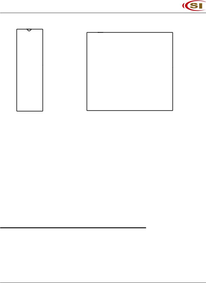
PIN CONFIGURATION |
PIN CONFIGURATION |
|
|
|
|
|
||||||||||||||||||
32-Pin SOP and DIP |
|
|
|
|
|
|
32-Pin 8x20mm TSOP-1 |
|
|
|
|
|
||||||||||||
|
|
|
|
|
|
|
|
|
|
|
|
|
|
|
|
|
|
|
|
|
|
|
|
|
|
NC |
|
1 |
32 |
|
|
VCC |
|
|
|
|
|
|
|
|
|
|
|
|
|
||||
|
|
|
|
|
|
|
|
|
|
|
|
|
|
|
|
|
||||||||
|
A16 |
|
2 |
31 |
|
|
A15 |
|
|
|
A11 |
|
1 |
32 |
|
OE |
||||||||
|
|
|
|
|
|
|
|
A9 |
|
2 |
31 |
|
A10 |
|||||||||||
|
A14 |
|
3 |
30 |
|
|
CE2 |
|
|
|
|
|
|
|||||||||||
|
|
|
|
|
|
|
|
|
|
|
|
|
|
|
|
|
||||||||
|
|
|
|
|
|
|
|
A8 |
|
3 |
30 |
|
CE1 |
|||||||||||
|
|
|
|
|
|
|
|
|
|
|
|
|
|
|
|
|
|
|||||||
|
A12 |
|
4 |
29 |
|
|
WE |
|
|
|
|
|
|
|
|
29 |
|
I/O7 |
||||||
|
|
|
|
|
|
|
A13 |
4 |
|
|||||||||||||||
|
A7 |
|
5 |
28 |
|
|
A13 |
|
|
|
|
|||||||||||||
|
|
|
|
|
|
|
|
|
|
|
|
28 |
|
I/O6 |
||||||||||
|
A6 |
|
6 |
27 |
|
|
A8 |
|
|
|
WE |
5 |
|
|||||||||||
|
|
|
|
|
|
|
|
|
|
|
|
27 |
|
I/O5 |
||||||||||
|
A5 |
|
7 |
26 |
|
|
A9 |
|
|
|
CE2 |
6 |
|
|||||||||||
|
|
|
|
|
|
|
|
|
|
|
|
26 |
|
I/O4 |
||||||||||
|
A4 |
|
8 |
25 |
|
|
A11 |
|
|
|
A15 |
7 |
|
|||||||||||
|
|
|
|
|
|
|
VCC |
|
8 |
25 |
|
I/O3 |
||||||||||||
|
A3 |
|
9 |
24 |
|
|
|
|
|
|
|
|
|
|
|
|
||||||||
|
|
|
|
|
OE |
|
|
|
|
|
|
|
NC |
|
9 |
24 |
|
GND |
||||||
|
|
|
|
23 |
|
|
A10 |
|
|
|
|
|
|
|||||||||||
|
A2 |
|
10 |
|
|
|
|
|
A16 |
|
10 |
23 |
|
I/O2 |
||||||||||
|
|
|
|
22 |
|
|
|
|
|
|
|
|
|
|
|
|
||||||||
|
A1 |
|
11 |
|
|
|
CE1 |
|
|
|
|
A14 |
|
11 |
22 |
|
I/O1 |
|||||||
|
|
|
|
21 |
|
|
I/O7 |
|
|
|
|
|
||||||||||||
|
A0 |
|
12 |
|
|
|
|
|
A12 |
|
12 |
21 |
|
I/O0 |
||||||||||
|
I/O0 |
|
13 |
20 |
|
|
I/O6 |
|
|
|
|
|
||||||||||||
|
|
|
|
|
|
|
|
A7 |
|
13 |
20 |
|
A0 |
|||||||||||
|
|
|
|
|
|
|
|
|
|
|||||||||||||||
|
|
|
|
|
||||||||||||||||||||
|
I/O1 |
|
14 |
19 |
|
|
I/O5 |
|
|
|
|
A6 |
|
14 |
19 |
|
A1 |
|||||||
|
|
|
|
|
|
|
|
|
|
|||||||||||||||
|
|
|
|
|
||||||||||||||||||||
|
I/O2 |
|
15 |
18 |
|
|
I/O4 |
|
|
|
|
A5 |
|
15 |
18 |
|
A2 |
|||||||
|
|
|
|
|
|
|
|
|
|
|||||||||||||||
|
GND |
|
16 |
17 |
|
|
I/O3 |
|
|
|
|
A4 |
|
16 |
17 |
|
A3 |
|||||||
|
|
|
|
|
|
|
|
|
|
|||||||||||||||
|
|
|
|
|
|
|
|
|
|
|
|
|
|
|
|
|
|
|
|
|
|
|
|
|
PIN DESCRIPTIONS |
|
|
|
|
|
|
|
|
|
|
|
|
|
|
|
|
|
|
||||||
|
A0-A16 |
|
Address Inputs |
|
|
|
|
|
|
|
|
|
|
|
|
|||||||||
|
|
|
|
|
|
|
|
|
|
|
|
|
|
|
|
|||||||||
|
CE1 |
|
Chip Enable 1 Input |
|
|
|
|
|
|
|
|
|
|
|
|
|||||||||
|
|
|
|
|
|
|
|
|
|
|
|
|
|
|
|
|||||||||
|
CE2 |
|
Chip Enable 2 Input |
|
|
|
|
|
|
|
|
|
|
|
|
|||||||||
|
|
|
|
|
|
|
|
|
|
|
|
|
|
|
|
|||||||||
|
OE |
|
Output Enable Input |
|
|
|
|
|
|
|
|
|
|
|
|
|||||||||
|
|
|
|
|
|
|
|
|
|
|
|
|
|
|
|
|||||||||
|
WE |
|
Write Enable Input |
|
|
|
|
|
|
|
|
|
|
|
|
|||||||||
|
|
|
|
|
|
|
|
|
|
|
|
|
|
|
||||||||||
|
I/O0-I/O7 |
Input/Output |
|
|
|
|
|
|
|
|
|
|
|
|
||||||||||
|
|
|
|
|
|
|
|
|
|
|
|
|
|
|
|
|
|
|
|
|
|
|||
|
Vcc |
|
Power |
|
|
|
|
|
|
|
|
|
|
|
|
|
|
|
|
|
|
|||
|
|
|
|
|
|
|
|
|
|
|
|
|
|
|
|
|
|
|
|
|
|
|||
|
GND |
|
Ground |
|
|
|
|
|
|
|
|
|
|
|
|
|
|
|
|
|
|
|||
|
|
|
|
|
|
|
|
|
|
|
|
|
|
|
|
|
|
|
|
|
|
|
|
|
OPERATING RANGE
Range |
Ambient Temperature |
VCC |
Commercial |
0°C to + 70°C |
5V ± 10% |
|
|
|
Industrial |
–40°C to + 85°C |
5V ± 10% |
|
|
|
TRUTH TABLE
Mode |
WE |
CE1 |
CE2 |
OE |
I/O Operation |
Vcc Current |
Not Selected |
X |
H |
X |
X |
High-Z |
ISB1, ISB2 |
(Power-down) |
X |
X |
L |
X |
High-Z |
ISB1, ISB2 |
|
|
|
|
|
|
|
Output Disabled |
H |
L |
H |
H |
High-Z |
ICC |
|
|
|
|
|
|
|
Read |
H |
L |
H |
L |
DOUT |
ICC |
Write |
L |
L |
H |
X |
DIN |
ICC |
|
|
|
|
|
|
|
Integrated Circuit Solution Inc. |
3 |
ALSR009-0A 5/7/2002
 Loading...