


 Loading...
0.8– 6 GHz 3V Downconverter
Technical Data
Features
•+0 dBm Input IP3 at 1.9 GHz
•Single +3V Supply
•8.5 dB SSB Noise Figure at
1.9GHz
•9.0 dB Conversion Gain at
1.9GHz
•Ultra-miniature Package
Applications
•Downconverter for PCS, PHS, ISM, WLL, and other Wireless Applications
Simplified Schematic
Surface Mount Package
SOT-363 (SC-70)
Pin Connections and
Package Marking
LO 1 |
|
|
|
|
91 |
|
|
|
|
6 |
IF and Vd |
|
|
|
|
|
|
|
|
|
|||||
GND |
2 |
|
|
|
|
|
|
5 |
GND |
|||
|
|
|
|
|
|
|||||||
RF |
3 |
|
|
|
|
|
|
|
|
SOURCE |
||
|
|
|
|
|
|
|
|
|
4 |
|||
|
|
|
|
|
|
|
|
|
|
|
|
BYPASS |
|
|
|
|
|
|
|
|
|
|
|
|
|
Note:
1. Package marking provides orientation and identification.
|
IF and Vd |
|
6 |
LO |
|
1 |
|
|
SOURCE |
|
BYPASS |
RF |
4 |
3 |
|
|
GROUND |
|
2, 5 |
7-135
IAM-91563
Description
Hewlett-Packard’s IAM-91563 is an economical 3V GaAs MMIC mixer used for frequency down-conver- sion. RF frequency coverage is from 0.8 to 6 GHz and IF coverage is from 50 to 700 MHz. Packaged in the SOT-363 package, this
4.0Ê sq. mm. package requires half the board space of a SOT-143 and only 15% the board space of an SO-8 package.
At 1.9 GHz, the IAM-91563 provides 9 dB of conversion gain, thus eliminating an RF or IF gain stage normally needed with a lossy mixer. LO drive power is nominally only -5 dBm, eliminating an LO buffer amplifier. The 8.5 dB noise figure is low enough to allow the system to use a low cost LNA. The -6 dBm Input IP3 provides adequate system linearity for most commercial applications, but is adjustable to 0 dBm.
The circuit uses GaAs PHEMT technology with proven reliability, and uniformity. The MMIC consists of a cascode FET structure that provides unbalanced gm modulation type mixing. An onchip LO buffer amp drives the mixer while bias circuitry allows a single +3V supply (through a choked IF port). The LO port is internally matched to 50 Ω. The RF and IF ports are high impedance and require external match-
ing networks.
5965-9973E

IAM-91563 Absolute Maximum Ratings
|
|
|
Absolute |
Symbol |
Parameter |
Units |
Maximum[1] |
Vd |
Device Voltage, RF output to ground |
V |
6.0 |
VRF, VLO |
RF voltage or LO voltage to ground |
V |
+0.5,-1.0 |
Pin |
CW RF Input Power |
dBm |
+13 |
Tch |
Channel Temperature |
°C |
150 |
TSTG |
Storage Temperature |
°C |
-65to150 |
IAM-91563 Electrical Specifications, TC = 25°C, Vd = 3V
Thermal Resistance[2]:
θch-c =310°C/W
Notes:
1.Permanent damage may occur if any of these limits are exceeded.
2.TC = 25°C (TC is defined to be the temperature at the package pins where contact is made to the circuit board).
Symbol |
Parameters and Test Conditions |
Units |
Min. |
Typ. |
Max. |
Std Dev[2] |
||
|
|
|
|
|
|
|
|
|
Gtest |
Gain in test circuit[1] |
RF=1890GHz,IF=250MHz |
dB |
4.0 |
9.0 |
|
|
|
NFtest |
Noise Figure in test circuit[1] |
RF=1890GHz,IF=250MHz |
dB |
|
8.5 |
11.0 |
|
|
Id |
Device Current |
|
|
mA |
6.0 |
9.0 |
12.0 |
|
|
|
|
|
|
|
|
|
|
NF |
Noise Figure (RF & IF with external matching, |
f = 0.9 GHz |
dB |
|
7.0 |
|
|
|
|
IF=250 MHz, LO power=-5 dBm) |
|
f = 1.9 GHz |
|
|
8.5 |
|
0.5 |
|
|
|
f = 2.4 GHz |
|
|
11.0 |
|
|
|
|
|
f = 4.0 GHz |
|
|
16.5 |
|
|
|
|
|
f = 6.0 GHz |
|
|
18.0 |
|
|
|
|
|
|
|
|
|
|
|
Gc |
Conversion gain (RF and IF with external matching, |
f = 0.9 GHz |
dB |
|
11.0 |
|
|
|
|
IF=250 MHz, LO power=-5 dBm) |
|
f = 1.9 GHz |
|
|
9.0 |
|
1.5 |
|
|
|
f = 2.4 GHz |
|
|
7.7 |
|
|
|
|
|
f = 4.0 GHz |
|
|
4.6 |
|
|
|
|
|
f = 6.0 GHz |
|
|
1.7 |
|
|
|
|
|
|
|
|
|
|
|
P1 dB |
Output power @ 1 dB compression (RF and IF with |
f = 0.9 GHz |
dBm |
|
-6.7 |
|
|
|
|
external matching, IF=250 MHz, LO power =-5 dBm) |
f = 1.9 GHz |
|
|
-8.0 |
|
1.3 |
|
|
|
|
f = 2.4 GHz |
|
|
-8.7 |
|
|
|
|
|
f = 4.0 GHz |
|
|
-15.0 |
|
|
|
|
|
f = 6.0 GHz |
|
|
-17.8 |
|
|
|
|
|
|
|
|
|
|
|
RLRF |
RF port return loss |
f = 0.5 - 6.0 GHz |
dB |
|
-1.7 |
|
0.2 |
|
|
|
|
|
|
|
|
|
|
RLLO |
LO port return loss |
f = 0.5 - 6.0 GHz |
dB |
|
-9.4 |
|
0.3 |
|
RLIF |
IF port return loss |
f = 50 - 700 MHz |
dB |
|
-3.7 |
|
0.2 |
|
|
|
|
|
|
|
|
|
|
IP3 |
Input Third Order Intercept Point |
RF = 1.9 GHz, IF = 250 MHz |
dBm |
|
-6.0 |
|
1.3 |
|
|
Id = 9.0 mA, LO power = -5 dBm |
|
|
|
|
|
|
|
IP3 |
Input Third Order Intercept Point |
RF = 1.9 GHz, IF = 250 MHz |
dBm |
|
0 |
|
1.1 |
|
|
Id = 15 mA, LO power = -2 dBm |
|
|
|
|
|
|
|
ISOLL-R |
LO-RF Isolation |
|
RF = 1.9 GHz |
dB |
|
18 |
|
|
|
|
|
|
|
|
|
|
|
ISOLR-I |
RF-IF Isolation (No Match) |
|
|
dB |
|
2 |
|
|
|
|
|
|
|
|
|
|
|
ISOLL-I |
LO-IF Isolation (No Match) |
|
|
dB |
|
4 |
|
|
Notes:
1.Guaranteed specifications are 100% tested in the circuit in Figure 18 in the Applications Information section.
2.Standard deviation number is based on measurement of at least 500 parts from three non-consecutive wafer lots during the initial characterization of this product, and is intended to be used as an estimate for distribution of the typical specification.
7-136

IAM-91563TypicalPerformance, TC = 25°C, Vd =3.0 V, RF=1890 MHz, LO = -5 dBm, IF=250 MHz, unless otherwise stated.
7-137
IAM-91563TypicalPerformance,TC = 25°C, Vd=3.0 V, RF=1890 MHz, LO = -5 dBm, IF=250 MHz,
unless otherwise stated.
SSB NOISE FIGURE (dB)
12
10
8
6
4
2
TA = +85°C
TA = +25°C
TA = -40°C
0 100 200 300 400 500 600 700
IF FREQUENCY (MHz)
CONVERSION GAIN (dB)
12
10
8
6
4
2
TA = 3.3V
TA = 3.0V
TA = 2.7V
0 100 200 300 400 500 600 700
IF FREQUENCY (MHz)
CONVERSION GAIN (dB)
12 |
|
|
|
|
|
|
|
|
|
|
|
|
|
|
|
|
|
|
|
|
|
|
|
|
|
|
|
|
|
|
|
|
|
|
|
10 |
|
|
|
|
|
|
|
|
|
|
|
|
|
|
|
|
|
|
|
|
|
|
|
|
|
|
|
|
|
|
|
|
|
|
|
8 |
|
|
|
|
|
|
|
|
|
|
|
|
|
|
|
|
|
|
|
|
|
|
|
|
|
|
|
|
|
|
|
|
|
|
|
6 |
|
|
|
|
|
|
|
|
|
|
|
|
|
|
|
||
|
|
|
|
|
|
T |
A = +85°C |
|
|
|
|
||||||
|
|
|
|
|
|
|
|
|
|
|
|||||||
|
|
|
|
|
|
|
|
TA = +25°C |
|
|
|
|
|||||
|
|
|
|
|
|
|
|
|
|
|
|
||||||
4 |
|
|
|
|
|
|
|
T |
A = -40°C |
|
|
|
|
|
|
||
|
|
|
|
|
|
|
|
|
|
|
|
|
|||||
|
|
|
|
|
|
|
|
|
|
|
|
|
|||||
2 |
|
|
|
|
|
|
|
|
|
|
|
|
|
|
|
|
|
|
|
|
|
|
|
|
|
|
|
|
|
|
|
|
|
|
|
0 |
100 |
200 |
300 |
400 |
500 |
600 |
700 |
||||||||||
IF FREQUENCY (MHz)
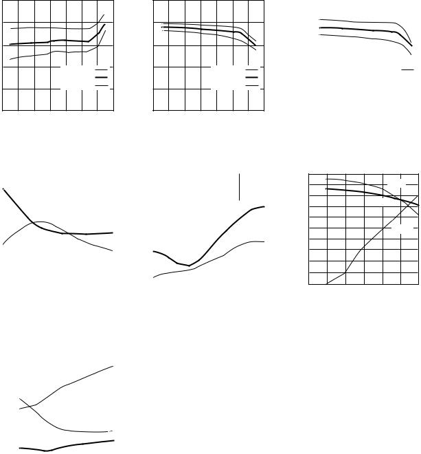
Figure 10. SSB Noise Figure vs. Frequency and Temperature.
Figure 11. Conversion Gain vs. Frequency and Supply Voltage.
Figure 12. Conversion Gain vs. Frequency and Temperature.
|
|
14 |
|
|
|
|
|
|
|
|
|
|
|
|
|
|
|
|
|
|
|
|
|
|
|
|
|
|
|
|
|
|
|
|
|
|
|
|
|
|
|
|
|
|
|
|
|
|
|
|
|
|
12 |
|
NF |
|
|
|
|
|
|
|
|
|
|
|
|
GAINCONVERSIONand |
FIGURENOISE(dB) |
|
|
|
|
|
|
|
|
|
|
|
|
|
|
|
|
|
|
|
|
|
|
|
|
|
|
|
|
|
|||
10 |
|
|
|
|
|
|
|
|
|
|
|
|
|
|
||
|
|
|
|
|
|
|
|
|
|
|
|
|
|
|
|
|
|
|
8 |
|
|
|
|
|
|
|
|
|
|
|
|
|
|
|
|
|
|
|
|
|
|
|
|
|
|
|
|
|
|
|
|
|
|
|
|
|
|
|
|
|
|
|
|
|
|
|
|
|
|
|
|
|
|
|
|
|
|
|
|
GAIN |
|
|
|
|
|
|
6 |
|
|
|
|
|
|
|
|
|
|
|
|
|
|
|
|
|
|
|
|
|
|
|
|
|
|
|
|
|
|
|
|
|
|
|
|
|
|
|
|
|
|
|
|
|
|
|
|
|
|
4 |
|
|
|
|
|
|
|
|
|
|
|
|
|
|
|
|
|
|
|
|
|
|
|
|
|
|
|
|
|
|
|
|
|
-10 -9 -8 -7 -6 -5 -4 -3 -2 -1 |
||||||||||||||
LO POWER (dBm)
Figure 13. Available Conversion Gain and Noise Figure vs. LO Drive Power.
(dBm) |
0 |
|
|
|
|
|
|
|
|
|
|
|
|
|
|
|
|
|
|
|
|
||
-2 |
|
|
|
|
|
|
IP |
3 |
|
|
|
3 |
|
|
|
|
|
|
|
|
|
|
|
IP |
-4 |
|
|
|
|
|
|
|
|
|
|
INPUT |
|
|
|
|
|
|
|
|
|
|
|
-6 |
|
|
|
|
|
|
|
|
|
|
|
and |
|
|
|
|
|
|
|
|
|
|
|
|
|
|
|
|
|
|
|
|
|
||
|
|
|
|
|
|
|
|
|
|
|
|
dB |
-8 |
|
|
|
|
|
|
P1 dB |
|
|
|
1 |
|
|
|
|
|
|
|
|
|||
P |
|
|
|
|
|
|
|
|
|
|
|
|
-10 |
|
|
|
|
|
|
|
|
|
|
|
|
|
|
|
|
|
|
|
|
|
|
|
-10 -9 -8 |
-7 -6 -5 -4 -3 -2 -1 |
|||||||||
LO POWER (dBm)
Figure 14. One dB Compression and Input Third Order Intercept vs. LO Drive Power.
|
0 |
|
|
|
|
|
|
|
-2 |
|
|
|
|
RF-IF |
|
Match) |
-4 |
|
|
|
|
|
|
-6 |
|
|
|
LO-IF |
|
||
|
|
|
|
|
|
||
No |
-8 |
|
|
|
|
|
|
(dB, |
-10 |
|
|
|
|
LO-RF |
|
ISOLATION |
-12 |
|
|
|
|
|
|
-14 |
|
|
|
|
|
|
|
-16 |
|
|
|
|
|
|
|
|
|
|
|
|
|
|
|
|
-18 |
|
|
|
|
|
|
|
-20 |
|
|
|
|
|
|
|
0 |
1 |
2 |
3 |
4 |
5 |
6 |
|
|
|
RF FREQUENCY (GHz) |
|
|||
Figure 15. Isolation (LO-RF, RF-IF, LO-IF) vs. Frequency with no RF and IF Matching Networks.
ISOLATION (dB)
0 |
|
|
|
|
|
|
|
|
|
|
|
|
|
|
|
|
|
|
|
|
|
|
|
|
|
|
|
|
|
|
|
|
|
-4 |
|
|
|
|
|
|
|
|
RF-LO |
|
|
|
|
|
||
|
|
|
|
|
|
|
|
|
|
|
|
|
||||
-8 |
|
|
|
|
|
|
|
|
|
|
|
|
|
|
|
|
|
|
|
|
|
|
|
|
|
|
|
|
|
|
|
|
|
-12 |
|
|
|
|
|
|
|
|
|
|
|
|
|
|
|
|
|
|
|
|
|
|
|
|
|
|
|
|
|
|
|
|
|
-16 |
|
|
|
|
|
|
|
|
|
|
|
|
|
|
|
|
|
|
|
|
|
|
|
|
|
|
|
|
|
|
|
|
|
-20 |
|
|
|
|
|
|
|
|
|
|
|
|
|
|
|
|
|
|
|
|
|
|
|
|
|
|
|
|
|
|
|
|
|
-24 |
|
|
|
|
|
|
|
|
|
|
|
|
|
|
|
|
|
|
|
|
|
|
|
RF-IF |
|
|
|
|
|
|
|||
|
|
|
|
|
|
|
|
|
|
|
|
|
||||
|
|
|
|
|
|
|
|
|
|
|
|
|
||||
-28 |
|
|
|
|
|
|
|
|
|
|
|
|
|
|
|
|
|
|
|
|
|
|
|
|
|
|
|
|
|
|
|
|
|
-32 |
|
|
|
|
|
|
|
|
|
|
|
|
|
|
|
|
|
|
|
|
|
|
|
|
|
|
|
|
|
|
|
|
|
|
|
|
|
|
|
|
|
|
|
|
|
|
|
|
|
|
-36 |
|
|
|
|
|
|
|
|
LO-IF |
|
|
|
|
|||
|
|
|
|
|
|
|
|
|
|
|
|
|||||
-40 |
|
|
|
|
|
|
|
|
|
|
|
|
|
|
|
|
|
|
|
|
|
|
|
|
|
|
|
|
|
|
|
|
|
0 |
1 |
2 |
3 |
|
4 |
|
|
5 |
6 |
|||||||
RF FREQUENCY (GHz)
Figure 16. Isolation (RF-LO, RF-IF, LO-IF) vs. Frequency with RF and IF Matching Networks.
7-138
IAM-91563 Typical Reflection Coefficients, TC = 25°C, ZO = 50 Ω, Vd =3 V
Frequency (GHz) |
RF (Mag) |
RF (Ang) |
LO (Mag) |
LO (Ang) |
IF (Mag) |
IF (Ang) |
0.1 |
|
|
0.43 |
-1 |
0.64 |
-8 |
0.2 |
|
|
0.39 |
-6 |
0.63 |
-9 |
0.3 |
|
|
0.39 |
-8 |
0.63 |
-10 |
0.4 |
|
|
0.39 |
-9 |
0.63 |
-10 |
0.5 |
|
|
0.39 |
-10 |
0.62 |
-11 |
0.6 |
|
|
0.39 |
-11 |
0.62 |
-12 |
0.7 |
|
|
0.40 |
-14 |
0.62 |
-13 |
0.8 |
0.91 |
-18 |
0.39 |
-14 |
|
|
0.9 |
0.91 |
-21 |
0.39 |
-16 |
|
|
1 |
0.91 |
-23 |
0.38 |
-17 |
|
|
1.1 |
0.92 |
-25 |
0.39 |
-17 |
|
|
1.2 |
0.91 |
-28 |
0.39 |
-19 |
|
|
1.3 |
0.88 |
-29 |
0.40 |
-22 |
|
|
1.4 |
0.87 |
-32 |
0.39 |
-22 |
|
|
1.5 |
0.85 |
-33 |
0.39 |
-24 |
|
|
1.6 |
0.84 |
-34 |
0.39 |
-25 |
|
|
1.7 |
0.83 |
-35 |
0.39 |
-26 |
|
|
1.8 |
0.82 |
-37 |
0.39 |
-27 |
|
|
1.9 |
0.82 |
-37 |
0.38 |
-29 |
|
|
2 |
0.81 |
-39 |
0.39 |
-29 |
|
|
2.1 |
0.81 |
-40 |
0.38 |
-31 |
|
|
2.2 |
0.81 |
-41 |
0.38 |
-31 |
|
|
2.3 |
0.81 |
-42 |
0.37 |
-32 |
|
|
2.4 |
0.81 |
-44 |
0.37 |
-33 |
|
|
2.5 |
0.80 |
-45 |
0.36 |
-34 |
|
|
2.6 |
0.80 |
-45 |
0.36 |
-35 |
|
|
2.7 |
0.81 |
-46 |
0.35 |
-36 |
|
|
2.8 |
0.81 |
-48 |
0.35 |
-36 |
|
|
2.9 |
0.81 |
-50 |
0.34 |
-37 |
|
|
3 |
0.82 |
-51 |
0.34 |
-37 |
|
|
3.1 |
0.83 |
-53 |
0.33 |
-38 |
|
|
3.2 |
0.83 |
-55 |
0.33 |
-39 |
|
|
3.3 |
0.83 |
-56 |
0.32 |
-39 |
|
|
3.4 |
0.85 |
-59 |
0.32 |
-40 |
|
|
3.5 |
0.86 |
-61 |
0.31 |
-40 |
|
|
3.6 |
0.87 |
-64 |
0.32 |
-42 |
|
|
3.7 |
0.85 |
-67 |
0.31 |
-42 |
|
|
3.8 |
0.83 |
-71 |
0.30 |
-45 |
|
|
3.9 |
0.83 |
-71 |
0.30 |
-43 |
|
|
4 |
0.82 |
-73 |
0.29 |
-46 |
|
|
4.1 |
0.83 |
-76 |
0.29 |
-45 |
|
|
4.2 |
0.83 |
-79 |
0.28 |
-47 |
|
|
4.3 |
0.84 |
-82 |
0.29 |
-48 |
|
|
4.4 |
0.84 |
-85 |
0.27 |
-49 |
|
|
4.5 |
0.84 |
-87 |
0.28 |
-50 |
|
|
4.6 |
0.85 |
-91 |
0.26 |
-51 |
|
|
4.7 |
0.84 |
-95 |
0.28 |
-52 |
|
|
4.8 |
0.85 |
-97 |
0.25 |
-52 |
|
|
4.9 |
0.85 |
-100 |
0.27 |
-54 |
|
|
5 |
0.85 |
-103 |
0.25 |
-54 |
|
|
5.1 |
0.86 |
-106 |
0.27 |
-57 |
|
|
5.2 |
0.85 |
-108 |
0.25 |
-56 |
|
|
5.3 |
0.84 |
-113 |
0.27 |
-58 |
|
|
5.4 |
0.84 |
-115 |
0.25 |
-58 |
|
|
5.5 |
0.84 |
-117 |
0.27 |
-61 |
|
|
5.6 |
0.83 |
-121 |
0.25 |
-61 |
|
|
5.7 |
0.83 |
-123 |
0.27 |
-64 |
|
|
5.8 |
0.81 |
-125 |
0.25 |
-65 |
|
|
5.9 |
0.81 |
-128 |
0.26 |
-67 |
|
|
6 |
0.80 |
-130 |
0.24 |
-65 |
|
|
7-139
Loading...