

HP ARMADA E500, ARMADA V300 User Manual

Notice
The information in this guide is subject to change without notice.
COMPAQ COMPUTER CORPORATION SHALL NOT BE LIABLE FOR
TECHNICAL OR EDITORIAL ERRORS OR OMISSIONS CONTAINED HEREIN;
NOR FOR INCIDENTAL OR CONSEQUENTIAL DAMAGES RESULTING FROM
THE FURNISHING, PERFORMANCE, OR USE OF THIS MATERIAL.
This guide contains information protected by copyright. No part of this guide may be
photocopied or reproduced in any form without prior written consent from Compaq
Computer Corporation.
© 2000 Compaq Computer Corporation.
All rights reserved. Printed in, U.S.A., U.K., Singapore, and Taiwan.
Compaq, Armada, and ROMPaq are registered in the U.S. Patent and
Trademark Office.
Microsoft, MS-DOS, Windows, Windows NT, and other names of Microsoft products
mentioned herein are trademarks or registered trademarks of Microsoft Corporation.
Intel, Pentium, and Celeron are trademarks of Intel Corporation. Imation and SuperDisk
are trademarks of Imation Corporation. CardWare is a registered trademark of Unicore
Software, Inc.
All other product names mentioned herein may be trademarks or registered trademarks
of their respective companies.
Software described herein is furnished under a license agreement or nondisclosure
agreement. The software may be used or copied only in accordance with the terms of
the agreement.
Technical Reference Guide
Compaq Armada E500 and Armada V300 Series
First Edition March 2000
Part Number 11QY-0200A-WWEN
Compaq Computer Corporation

preface
EFERENCE DOCUMENTS
R
The following reference documentation and web addresses provide information for the
Compaq Armada E500 and Armada V300 computers:
Compaq Specification
■
#333116,
#353918,
#342609,
#387046,
#290725,
#353924,
#258896,
■
Compaq Armada E500 and Armada V300 Maintenance and Service Guide
■
Microsoft Operating System Manual
■
Synaptics Touchpad Interfacing Guide
Compaq Web site at http://www.compaq.com
■
Modem commands at http://www.compaq.com/support/portables
■
ATI Rage Mobility-P Video Controller
TI PCI1450 Cardbus Controller
ESS 1978SF Maestro-2E Audio Controller
SMSC MSIO, SMSC37N971, Tikki
Flash ROM,512k x 8, 60ns, 5V
ESS 1920 Audio Codec
Li-Ion Battery Specification
2HAB=?A
LEE

ONTENTS
C
chapter 1
S
YSTEM ARCHITECTURE
Standard Features.............................................................................................................................1-2
External Ports/Connectors ...............................................................................................................1-4
Power Management..........................................................................................................................1-4
System Architecture.........................................................................................................................1-5
Mechanical..................................................................................................................................... 1-11
Docking Support............................................................................................................................1-11
Security Features............................................................................................................................1-12
chapter 2
P
ROCESSOR
Host Bus (Northbridge)....................................................................................................................2-1
ISA Bus (Southbridge)...................................................................................................................2-10
Clocks............................................................................................................................................. 2-16
chapter 3
S
YSTEM MEMORY
Base System Memory ...................................................................................................................... 3-1
System Memory Expansion............................................................................................................. 3-2
, C
ACHE AND SYSTEM SUPPORT
chapter 4
PC C
ARD INTERFACE
Functional Description.....................................................................................................................4-1
CardBus Controller..........................................................................................................................4-1
System Block Diagram .................................................................................................................... 4-3
PCI Interface .................................................................................................................................... 4-3
PC Card Applications Overview......................................................................................................4-4
Programmable Interrupt Subsystem.................................................................................................4-6
Power Management Overview.......................................................................................................4-10
Table of Contents
EEE

chapter 5
S
I/O C
UPER
ONTROLLER
8051 Microcontroller.......................................................................................................................5-3
Real-Time Clock and CMOS RAM.................................................................................................5-4
Diskette Controller...........................................................................................................................5-4
Parallel Port......................................................................................................................................5-5
GPIO Usage .....................................................................................................................................5-6
2
I
C Controller...................................................................................................................................5-6
Serial UARTs...................................................................................................................................5-7
Shared Flash ROM Interface ...........................................................................................................5-7
Keyboard Scan................................................................................................................................. 5-8
PS/2 Serial Mouse/Keyboard Interfaces..........................................................................................5-8
chapter 6
A
UDIO SUBSYSTEM
Functional Description.....................................................................................................................6-1
Features ............................................................................................................................................ 6-3
Power Management..........................................................................................................................6-3
WaveCache ......................................................................................................................................6-5
Audio Docking Solution.................................................................................................................. 6-6
ES1921 Audio CODEC ................................................................................................................... 6-6
Functional Description.....................................................................................................................6-8
Digital Interface ............................................................................................................................. 6-11
Power Management........................................................................................................................6-14
Audio Linear Amplifier LM4873..................................................................................................6-15
chapter 7
V
IDEO/GRAPHICS SUBSYSTEM
General Features...............................................................................................................................7-1
Video Interface................................................................................................................................. 7-2
Bus Interface .................................................................................................................................... 7-3
Power Management..........................................................................................................................7-3
Video Controller Clock Generation.................................................................................................7-3
Flat Panel Support............................................................................................................................7-4
CRT.................................................................................................................................................. 7-4
2D Acceleration ............................................................................................................................... 7-4
3D Acceleration ............................................................................................................................... 7-5
TV Out .............................................................................................................................................7-5
Simultaneous Scan Mode................................................................................................................. 7-7
Video Mode Support........................................................................................................................7-7
Video Memory............................................................................................................................... 7-11
Zoomed Video................................................................................................................................7-11
Motion Video Acceleration............................................................................................................7-12
chapter 8
K
EYBOARD/POINTING DEVICE SUBSYSTEM
Internal Keyboard ............................................................................................................................8-1
Touchpad Interface ..........................................................................................................................8-1
EasyPoint IV (Pointing Stick)..........................................................................................................8-2
EL
Table of Contents

Hotkeys ............................................................................................................................................8-2
External Keyboard/Mouse Communications...................................................................................8-3
chapter 9
P
OWER SUPPLY
DC/DC Converter ............................................................................................................................9-2
Smart Battery ...................................................................................................................................9-3
Display Inverter................................................................................................................................ 9-4
External AC Adapter........................................................................................................................ 9-4
Power Management Controller........................................................................................................9-5
chapter 10
M
ASS STORAGE
Hard Drive Subsystem...................................................................................................................10-1
Diskette Drive Subsystem..............................................................................................................10-3
CD-ROM Module..........................................................................................................................10-3
DVD-ROM Module....................................................................................................................... 10-3
SuperDisk LS-120 Drive Subsystem.............................................................................................10-4
chapter 11
I
NTERNAL MODEM
Combination Card Overview (Lucent Chipset).............................................................................11-1
Global Mini-PCI Modem Card (Lucent Chipset)........................................................................11-10
Table of Contents
L

appendix A
D
OCKING
Docking Sequence........................................................................................................................... A-1
Docking Interface............................................................................................................................ A-1
appendix B
P
OWER CONSERVATION
Power Management States...............................................................................................................B-1
Processor Power Management.........................................................................................................B-3
Processor Thermal Management......................................................................................................B-4
Secondary Cache Power Management ............................................................................................B-4
PCI Bus Power Management...........................................................................................................B-4
Video Power Management...............................................................................................................B-5
Hard Drive and Bay Power Management........................................................................................B-5
MSIO Super I/O Power Management..............................................................................................B-5
Audio Power Management ..............................................................................................................B-5
..........................................................................................................................................................I-1
I
NDEX
LE
Table of Contents
chapter
1
YSTEM ARCHITECTURE
S
The Compaq Armada E500 and Armada V300 Series offer Intel Mobile Pentium II, III
or Celeron Processors with 32-bit or 64-bit architecture, MMX technology, and level-2
cache memory. Both Armada E500 and Armada V300 Series provide desktop
functionality and connectivity through optional expansion bases or convenience bases.
Depending on the Armada E500 computer model, the following processors are used:
a 366- or 400-MHz Intel Mobile Pentium II Processor with 256-KB integrated L2
■
cache, or
a 450-, 500-, or 600-MHz Intel Mobile Pentium III Processor with 256-KB
■
integrated L2 cache.
Depending on the Armada V300 computer model, a 400- or 466-MHz Intel Celeron
Processor with 128-KB integrated L2 cache is used.
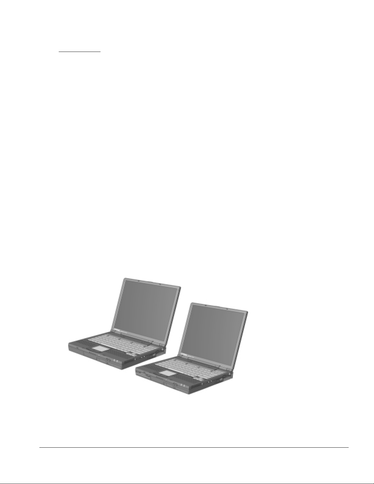
The computers, shown in Figure 1-1, dock with the Compaq ArmadaStation EM
(Armada E500 only), Armada MiniStation E/EX (Armada E500 only), Convenience
Base or Port Replicator.
Figure 1-1.
Compaq Armada E500 and Armada V300 Personal Computers
System Architecture
1-1

Standard Features
The computers have the following features:
The following processors are available, varying by computer model:
■
The Armada E500 features an Intel Mobile Pentium III 450-, 500-, or 600-MHz
■
Processor or Intel Mobile Pentium II 366- or 400-MHz Processor, with 256-KB
integrated cache.
The Armada V300 features an Intel Celeron 400- or 466-MHz Processor, both
■
with 128-KB integrated L2 cache.
ATI Mobility P video controller, with 8-MB (Armada E500) and 4-MB (Armada
■
V300) SGRAM (synchronous graphics)
The following standard memory is available, varying by computer model:
■
The Armada E500 is equipped with 64-MB high-performance Syncheronous
■
DRAM (SDRAM), expandable to 512 MB.
The Armada V300 is equipped with 64- or 32-MB high-performance SDRAM,
■
expandable to 512 MB.
Microsoft Windows 95, Window 98 or Windows NT Workstation 4.0 preinstalled
■
The following displays are available, varying by computer model:
■
The Armada E500 features a 15-inch or 14.1-inch, XGA, TFT (1024 × 768) or
■
12.1-inch, SVGA, TFT (800 × 600) display, both with over 16.8 million colors.
The Armada V300 features a 14.1-inch XGA TFT (1024 × 768), 12.1-inch
■
SVGA TFT (800 × 600), or 12.1-inch SVGA STN (800 × 600) display, all with
over 16.8 million colors.
The following keyboards are available, varying by computer model:
■
The Armada E500 provides a TouchPad or pointing stick keyboard.
■
The Armada V300 is equipped with a TouchPad keyboard.
■
Mini PCI 56K V.90 modem, optional Mini PCI V.90 modem plus 10/100 NIC
■
combination card.
The following PC Card features are available, varying by computer model:
■
The Armada E500 features two Type II PC Card slots with support for both
■
32-bit CardBus and 16-bit PC Cards; Zoomed video is supported in the
bottom slot.
The Armada V300 features one Type II PC Card slot with support for both
■
32-bit CardBus and 16-bit PC Cards.
External AC adapter with power cord
■
The following battery packs are available, varying by computer model:
■
The Armada E500 supports a 9- or 6-cell Lithium Ion (Li-ion) primary
■
battery pack in the battery bay or DualBay, and a 6-cell Li-ion MultiBay battery
pack in the MultiBay; supporting up to three battery packs in the computer at
one time.
1-2
System Architecture
The Armada V300 supports a 9- or 6-cell Li-ion primary battery pack in the
■
battery bay and a 6-cell Li-ion MultiBay battery pack in the MultiBay.

The following hard drives are available, varying by computer model:
■
The Armada E500 supports a 12.0-, 6.0-, or 4.3-GB high-capacity SMART hard
■
drives with DriveLock security and Prefailure Warranty.
The Armada V300 supports a 6.0- or 4.3-GB high-capacity SMART hard drives
■
with DriveLock security and Prefailure Warranty.
Flexible MultiBay that accommodates a 24X MAX CD-ROM drive, DVD-ROM
■
drive, SuperDisk LS-120 drive, 6-cell Li-ion MultiBay battery pack, or secondary
hard drive (when used with a Hard Drive MultiBay Adapter).
Armada E500 provides a DualBay that accommodates a diskette drive or a second
■
battery pack.
Connectors for parallel, serial, audio in/out, external monitor, universal serial bus,
■
external keyboard, and AC power.
Stereo speakers providing Compaq PremierSound 16-bit stereo sound.
■
Energy Star-compliant power saving features.
■
Security features, including power-on, keyboard, setup, and DriveLock passwords.
■
Desktop expandability available with the optional Compaq Armada Station EM and
■
Compaq Convenience Base.
System Architecture
1-3

External Ports/Connectors
Standard 176-pin Armada docking connector
■
Fast IR port
■
One or two CardBus slots with support for Zoomed Video
■
Audio connectors for speaker or headphones out, and microphone in
■
PS/2 port for mouse or external keyboard with support for Y–cable for two devices
■
RJ-11 modem jack with internal connection to modem slot, depending on model
■
RJ-45 Ethernet jack with internal connection to the combination modem/LAN slot,
■
depending on model
One standard 15-pin VGA connector with support for DDC-2B monitor detection
■
One standard 9-pin serial port connector
■
One standard 25-pin parallel port connector with support for ECP, EPP,
■
bidirectional, and standard mode
One low-power USB port with standard Type–A connector
■
Power Management
Advanced Power Management (APM) version 1.2 compliant
■
Advanced Configuration and Power Management (ACPI) version 1.0 compliant
■
Support for Suspend (S1), Suspend-to-RAM (S3), and Suspend-to-Disk (S4)
■
Power management settings can be customized by the user
■
Hotkeys for setting performance level versus battery life
■
Smart batteries that provide an accurate battery power gauge
■
Dock device power management
■
Active Thermal Feedback (ATF) support
■
Lid switch suspend/resume
■
Power/Suspend button with system override
■
1-4
System Architecture

System Architecture
The system architecture is shown in Figure 1-2.
Coppermine or
Dixon CPU
4/8MB
SDRAM
Video ATI
Mobility-P
SVGA LCD
Display
CRT
Figure 1-2.
Base SODIMM
User SODIMM
Mini-PCI Modem
ESS Audio
HDD
CD
AC97
USB Port
Flash ROM
Keyboard
Infrared
Touchpad
440BX
North Bridge
PCI BusAGP Bus
PIIX4
PCI-IDE
South Bridge
USB Control
PCI-ISA
Tikki MSIO
PS/2
Serial
Parallel
Floppy
ROM
Compaq Armada E500 and Armada V300 Block Diagram
RJ-11
RJ-45
Cardbus
Controller
TI1225
Slot1
Slot2
Docking
Station
Moon PCI-PCI
Bridge
AC97
USB
Floppy
Serial
Parallel
PS/2
The system is made up of four main buses: the host bus, the AGP bus, the PCI bus, and
the ISA bus. The Intel 440BX chipset controls all four buses. The 82440 interfaces the
host bus to the AGP and PCI buses and is referred to as the Northbridge. The PIIX4E,
used with the PII, or the PIIX4M, used with the PIII, interfaces from the PCI bus to the
ISA bus and is referred to as the Southbridge.
The host bus is connected to:
Celeron, Pentium II, or Pentium III processor
■
Secondary cache (L2)
■
Northbridge chipset (82440BX)
■
System Architecture
1-5

The AGP bus is connected to:
Northbridge chipset (82440BX)
■
Video controller (ATI RAGE Mobility-P)
■
System SDRAM
■
The PCI bus is connected to:
Northbridge chipset (82440BX)
■
Southbridge chipset (PIIX4M)
■
CardBus controller
■
Audio subsystem
■
The ISA bus is connected to:
Southbridge chipset (PIIX4M)
■
Flash ROM
■
Super I/O controller (MSIO)
■
CPU
Armada E500:
366- or 400-MHz Intel Mobile Pentium II Processor
■
450-, 500-, or 600-MHz Intel Mobile Pentium III Processor
■
Armada V300:
400- or 466-MHz Intel Celeron Processor with 128-KB integrated L2 cache
■
Chipset
Intel 82440BX Northbridge
Support for all Intel Mobile Pentium II and Pentium III Processors
■
Unbuffered and registered SDRAM support (×-1-1-1 access at 66 to 100 MHz)
■
Enhanced SDRAM Open Page Architecture support for 16- and 64-Mbit DRAM
■
devices with 2-, 4-, and 8-Kbyte page sizes
PCI bus interface
■
PCI revision 2.1, 3.3-volt, 33-MHz interface compliant
■
PCI Parity Generation support
■
Data streaming support from PCI to DRAM
■
Delayed transaction support for PCI-DRAM reads
■
1-6
System Architecture

AGP interface
■
Integrated DRAM controller supports single AGP-66/133 compliant device (3.3
■
volt)
AGP Specification revision 1.0 compliant
■
AGP data/transaction flow optimized arbitration mechanism
■
AGP side–band interface for efficient request pipelining
■
AGP specific data buffering
■
Supports concurrent CPU, AGP, and PCI transactions to main memory
■
AGP high-priority transaction support
■
Advanced power management features
■
Supports Standby (S1), Suspend-to-DRAM (S3), and Suspend-to-Disk (S4)
■
Static stop clock support
■
Dynamic power-down of idle DRAM rows
■
SDRAM self-refresh power-down support in suspend mode
■
Stop clock grant and halt special cycle translation (host to PCI Bus)
■
Advanced Configuration and Power Interface (ACPI)–compliant power
■
management
492-pin BGA package
■
3.3-volt core and mixed 3.3-volt and GTL I/O
■
Interfaces directly to the PIIX4M
■
Intel PIIX4M Southbridge
3.3-volt with 5-volt tolerance
■
PCI-to-ISA bridge
■
Supports full ISA or Extended I/O (EIO) bus in positive decode or subtractive
■
decode
Supports PCI DMA with three PC/PCI channels and Distributed DMA
■
protocols (simultaneously)
Supports serialized IRQ protocol
■
PCI revision 2.1 specification compliant
■
Built-in real-time clock with wake-on-alarm capability (ACPI/OnNow compliant)
■
SMBus interface
■
System Architecture
1-7

Advanced Power Management support
■
3.3-volt operation with 5-volt tolerant buffers
■
Power-On Suspend (S1), Suspend-to-DRAM (S3), Suspend-to-Disk (S4), and
■
Soft-Off (S5) System States
All registers readable and restorable for proper resume from zero-volt suspend
■
Global and local device management
■
Supports thermal alarm
■
Support for external microcontroller
■
Full support for ACPI revision 1.0 specification and OS directed power
■
management
Integrated IDE controller with Ultra-DMA-33 support
■
Integrated 12 × 32-bit buffer for IDE PCI burst transfers
■
Two hot-swappable USB channels with legacy keyboard/mouse support
■
324-pin mBGA package
■
DRAM
64-MB synchronous DRAM (SDRAM) memory onboard
■
Two SO-DIMMs (Bank 1 and 2)
■
All DRAM is 3.3-volt 66-MHz or faster self-refreshing SDRAM
■
PCI Bus Devices
All internal PCI buses and PCI components operate at 3.3 volt.
NOTE:
CardBus controllers
■
TI225
Support for Zoomed Video slot
■
Support for serialized ISA IRQs
■
Supports two PC Card/CardBus slots (one PC Card slot for Aramada V300) with
■
hot removal/insertion
Burst transfers to maximize data throughput on the PCI/CardBus bus
■
Supports distributed DMA and PC/PCI DMA
■
Supports ring indicate
■
1-8
System Architecture

Video Controller
■
ATI RAGE Mobility-P
32-bit wide memory-mapped registers
■
Advanced Graphics Platform (AGP) 2X bus with sideband support; 133-MHz
■
throughput
Floating-Point Setup Engine for high-performance 3D and CAD
■
Motion compensation for full-screen MPEG-2 video without external acceleration
■
hardware
4 or 8-MB, 3.3-volt 125-MHz video SDRAM
■
Support for Zoomed Video
■
Built-in support for LVDS data bus to LCD display
■
Built-in NTSC and PAL video output (composite)
■
Simultaneous display of CRT+LCD+TV including separate images
■
DDC 2B support for external monitors
■
Advanced power management features (automatic power-down, standby, and
■
panel-off)
Audio
■
ESS Maestro 2E/ES1921 CODEC
Hot docking 6-pin interface to expansion audio mixer (ES978)
■
Monophonic full duplex using two DMA channels
■
Self-timed joystick port
■
I2S interface to internal stereo D/A for external ZV port
■
Complete general interrupt mapping, including sharing of all interrupts
■
Stereo 16-bit, Wavetable and FM synthesizers, MPU-401 MIDI support
■
ISA Bus Devices
All internal ISA buses and ISA components operate at 3.3-volt.
NOTE:
BIOS ROM
■
Intel 28F004BV
4-MB boot block flash ROM
■
System Architecture
1-9

SMC Super I/O Controller
■
SMC FDC37N97X
Simultaneous support for three PS/2 ports (1 internal + 2 external)
■
Advanced infrared communications controller
■
ACPI Embedded Controller Interface
■
High-performance, embedded 8051 keyboard and system controller
■
Low Suspend current in sleep mode
■
System power plane control and power sequencing
■
Battery management interface for charging and smart battery fuel gauge
■
Active thermal interface for CPU thermal management
■
1.44-MB Super I/O FDC controller
■
IEEE 1284 parallel port
■
Serial infrared support: IrDA version 1.1 (4 Mbps)
■
Full Plug-and-Play support
■
High speed NS16550A-compatible UART with 16-byte send/receive FIFOs
■
Real-time clock
■
■
Modem/LAN
Mini-PCI Modem or Combination Modem/NIC Card
Internal Mini-PCI Type-1B slot
■
Flexible method of supporting an internal modem or modem/LAN combo card
■
with the least amount of difficulty surrounding European modem approvals
Slot supports only Compaq-approved cards
■
1-10
System Architecture

Power Subsystem
System DC/DC
■
Based on the MAX1630
■
Provides a stable 3.3 to 5.0 volts from a DC source of 9 V to 19 V
■
AC Cube
■
Provides 18.5 volts DC +/- 3.75% at 100 to 240 volts AC
■
50 watts output
■
6 or 9-cell Li-ion battery in dedicated bay; only Armada E500 and Armada V300-
■
specific batteries can be inserted into the primary bay due to mechanical keying
Mechanical
Size: 9.9-in (252 mm) × 12.36-in (314 mm) × 1.65-in (42 mm)
■
Weight: 5,5 to 7.5 pounds (2.6 to 3.2 kg)
■
Construction: 2.3 mm wall thickness using polycarbonate
■
Features:
■
One MultiBay for SuperDisk LS-120 drive, DVD-ROM drive or second hard
■
drive; one DualBay that can be used for a diskette drive/battery on the Armada
E500; one fixed diskette drive on the Armada V300
Removable main hard drive
■
Easy-to-access memory upgrades
■
Ergonomic design
■
Docking Support
ArmadaStation EM Support (Armada E500 only)
One serial port
■
One parallel port
■
Two PS/2 ports to connect an external keyboard and a pointing device
■
One XGA CRT port (replicates computer port)
■
Three PCI slots for Compaq-approved PCI add-in cards
■
Dual MultiBays
■
One half-height bay
■
An additional dual-channel, PCI-based IDE controller, to connect HDD, CD-ROM,
■
DVD-ROM,or other peripherals
Audio line-in, microphone-in, speaker/headphones-out
■
Additional audio speaker
■
Two USB ports
■
System Architecture
1-11

Convenience Base
One serial port
■
One parallel port, with support for an Armada 4100/7800-compatible diskette drive
■
option (Note: The Armada E500 and Armada V300 do not support this, but the
Convenience Base does.)
Two PS/2 ports to connect one for an external keyboard and a pointing device
■
One XGA CRT port (replicates computer port)
■
One PCI slot capable of supporting Compaq-approved LAN adapters
■
Audio line-in, microphone-in, speaker/headphones-out
■
Two USB ports
■
Port Replicator
One serial port
■
Two PS/2 ports to connect an external keyboard and a pointing device
■
One XGA CRT port (replicates computer port)
■
Audio line-out
■
One USB port
■
DC power-in (pass through)
■
Security Features
These security management features customize system security:
Power-On and Setup Passwords—prevent unauthorized access to information and
■
computer configuration.
DriveLock—prevents unauthorized access to hard drives.
■
Device disabling—prevents unauthorized data transfer through modems, serial ports,
■
parallel ports, and infrared ports on the computer and an optional docking station.
QuickLock/QuickBlank—locks the keyboard and clears the screen.
■
Ownership Tag—displays ownership information during system restart.
■
1-12
System Architecture

chapter
2
PROCESSOR, CACHE, AND
SYSTEM SUPPORT
Host Bus (Northbridge)
The Armada E500 and Armada V300 computers use the Intel Pentium II, Pentium III,
and Celeron Processors, respectively. The Pentium Processors feature:
450-, 500-, or 600-MHz CPU with 100-MHz SDRAM bus for PIII, 66MHz for PII
Integrated L2 cache running at processor speed
MMX-2 instruction set
SpeedStep desktop operation (PIII)
Pentium II or III CPU/Cache
The computers use the Intel Pentium II or III Processor technology housed in a BGA
package. The PII and PIII differ in substantial ways (66-MHz bus instead of a 100MHz bus, integrated GTL resistors) so that a common PII and PIII printed circuit board
is impossible. A general feature list is as follows:
Full SMI (System Management Interrupt)
Fully static (support Stop grant and Stop clock states)
66- (PII) or 100-MHz (PIII) bus interface to the system
32-bit address bus
64-bit data bus
256-KB on-chip cache (Armada E500 PII and PIII); 128-KB on-chip cache (Armada
V300)
Capability of executing two instructions per clock through two pipelined integer
units
Multimedia extension (MMX) register set
Processor, Cache, and System Support 2-1

The PII Processor has integrated 256 K L2 cache on the die designed using 0.18 micron
process technology. It is offered at 400- and 466-MHz with 66-MHz system bus speed.
It’s core design consists of an integrated L2 cache controller and a 64-bit high
performance system bus. The on-die L2 cache complements the system bus by
providing critical data faster, improving performance, and reducing total system power
consumption. The PII Processor’s 64-bit wide low power GTL+ system bus is
compatible with the 440BX PCIset and provides a glueless, point to point interface for
an I/O bridge/memory controller.
The Intel Pentium III Processor also implements 0.18 micron process technology with
Katmai New Instructions. It has a 100 MHz bus and uses the PIIX4M and 440BX
chipset with 100 MHz SDRAM.
The new Intel SpeedStep technology allows the PIII Processor to run at either notebook
or desktop frequencies. At the higher frequency, a higher voltage must also be run. For
the Armada E500, the notebook frequency is 500 MHz at 8 watts, and the desktop
frequency is 650 MHz at 14 watts. The high power mode may be operated under
battery or AC power, but the battery life will be lower and the acoustic noise higher
than operation in the normal notebook mode.
The Intel PII and PIII Processors are fully compatible with the entire installed base of
applications for DOS, Windows, OS/2, and UNIX. Superscalar architecture, branch
prediction, and separate code and data caches all provide increased performance over
previous X86 Processors. Reduced voltage operation and enhanced power management
features are provided.
82440BX
The Intel 440BX PCI-based chipset is optimized for portable systems with stringent
form-factor and power-consumption requirements. It consists of two components–the
82440BX and the PIIX4M. The 82440BX is referred to as the Northbridge (control
between the PCI bus and the CPU and AGP buses). The PIIX4M is referred to as the
Southbridge (control between the PCI bus and the ISA bus). The remainder of this
section involves the 82440BX.
The 82440BX integrates the CPU, AGP, PCI, and DRAM bus interfaces. This includes
the DRAM controller, AGP bus arbiter, PCI bus arbiter, power management, and the
host (CPU) interface.
The 82440BX’s data buffer steers and buffers data between the four interfaces: 64-bit
CPU, 64-bit DRAM, 32-bit AGP, and 32-bit PCI. The data flow can be CPU-to-PCI,
CPU-to-AGP, CPU-to-DRAM, AGP-to-DRAM, or PCI-to-DRAM.
2-2 Processor, Cache, and System Support

Power Planes
The 82440BX supports suspend modes: Power-On-Suspend (POS), Suspend-To-RAM
(STR) and Suspend-To-Disk (STD). The 82440BX maintains leakage control so that
back powering of other system functions cannot occur in Suspend. Table 2-1 lists the
82440BX power planes.
Table 2-1
82440BX Power Planes
Plane VCC OPTIONS Selection Description
VCC 3.3 V BXVCC3 Main power pin at 3.3 V
VCCAGP 3.3 V BXVCC3 AGP bus power
GTLREFA,B 0.55 VTT VBXGTLREF GTL buffer voltage reference input
VTTA,B CPU selected VBXGTL GTL threshold (clamp) voltage
REFVCC5 3.3 V BXVCC3 PCI 5 V tolerant level (not used)
Reset Interface
The 82440BX reset function is an integral part of the Suspend/Resume functions. The
82440BX supports the normal reset function in a desktop platform, as well as various
power-up reset and resume reset functions in the mobile platform.
The PIIX4M integrates the system reset logic for the system. The PIIX4M generates
PCIRST# and RSTDRV during power up (PWROK), when a hard reset is initiated
through the RC register, and during certain power management resume operations.
The 440BX chipset has two separate reset inputs: RCIN# and PWROK; and four reset
outputs: PCIRST#, CPURST#, SUS_STAT#, and INIT#.
PWROK: An RC delay from the enabling of SYSVCC3. During the period when
RCRST# is de-asserted and PWROK is not yet asserted, RSTDRV and CPURST# are
asserted. When PWROK becomes asserted, RSTDRV and CPURST de-assert, causing
a system reset.
Processor, Cache, and System Support 2-3

Table 2-2
440BX Reset Outputs
Signal Assert w/
PCIRST#
PCIRST# - PCI bus, 82440BX, NB,
CPURST# Always CPU 82440BX CPU reset signal.
RSTDRV Always ISA bus / X-Bus
SUSSTAT# N/A PIIX4M Only SUSSTAT# signals a Suspend
INIT# No CPU PIIX4M CPU soft reset generated by
System Devices or
Buses Affected
PIIX4M
devices
Source Description
PIIX4M Used in power-up sequence,
resume from STR or STD.
PIIX4M ISA bus reset. Directly derived
from PCIRST#. Resides in PIIX4M
main voltage well.
mode entry/exit. This signal
originates from the PIIX4M
Suspend voltage well.
PIIX4M.
CPURST# is generated by the 82440BX in the following instances:
CPURST# is always asserted if PCIRST# is asserted.
CPURST# is asserted during resume sequence from POS (CRst_En= 1).
The 82440BX de-asserts CPURST# 1 ms after detecting the rising edge of PCIRST#.
The CPURST# is synchronous to the host bus clock.
The PCIRST# must be asserted when the system resumes from low power mode, in
which power is removed, including resume from Suspend-to-RAM or Suspend-to-Disk
and power-up sequence. In these cases, CPURST# is activated with the assumption that
CPU power is removed to enforce correct resume sequence.
When resuming from POS, the PCIRST# and CPURST# typically are not used to speed
up the resume sequence. In this case, the option to reset the CPU is available by using
the CRst_En configuration bit option.
When a soft reset is initiated, the PIIX4M drives SUSTAT# to the 82440BX. This
forces the 82440BX to switch to a Suspend refresh state. The 82440BX cannot accept
BIOS attempts to execute cycles to DRAM because it believes it is in a Suspend state.
After coming out of reset, software must set the Normal refresh enable bit (bit 4, Power
Management Control register at Offset 7Ah) in the 82440BX before accessing
memory.
2-4 Processor, Cache, and System Support

Power-On Configuration
The 440BX chipset uses power-on registers to define system configuration variables
that must be set by hardware options. All signals used to select power-on options are
connected to either internal pull-down or pull-up resistors of minimum 50 K/maximum
150 K ohms. These resistors select a default mode on the signal during reset.
To enable different modes, external pull-up or pull-down resistors (the opposite of the
internal resistors) of approximately 10 K ohm can be connected to particular signals.
These resistors are connected to the +3.3-volt power supply. During normal operation
of the 82440BX–including while it is in Suspend mode–the paths from GND or + 3.3
volts to the internal strapping resistors are disabled to effectively disable the resistors.
In these cases, the MAB# lines are driven by the 82440BX to a valid voltage level.
Table 2-3 lists the Power-On options that are loaded into the 82440BX during cold
reset. The 82440BX is required to float all the signals connected to straps during cold
reset and keep them floated for a minimum of four host clocks after the end of cold
reset sequence.
Table 2-3
82440BX Power-On Options During Cold Reset
Line Setting Description Notes
MAB13# - Reserved
MAB12# 0 Host frequency select 0 ***= 60/66 MHz, 1 **= 100 MHz
MAB11# 1 In-order queue depth enable 0 = non-pipelined, 1 ** = pipelined (8-deep)
MAB10 0 Quick start select 0 ** = normal mode, 1 = Quick start mode
MAB9# 0 AGP disable 0 ** = AGP enabled, 1 = AGP disabled
MAB8# - Reserved
MAB7# 0 Memory module configuration 0 ** = normal (BX), 1 = 430TX-compatible
MAB6# 1 Host bus buffer mode select 0 ** = desktop GTL+, 1 = mobile GTL+
**
default selection *** default on P-II versions ** default on P-III versions
When resuming from Suspend, even while PCIRST# is active, the MAB# lines remain
driven by the 82440BX and the strapping latches maintain the value stored during the
cold reset.
Processor, Cache, and System Support 2-5

Clock Interface
The 82440BX requires two clock inputs which are CPUCLK (66 or 100 MHz) and
PCICLK_440BX (33 MHz). The CPUCLK signal is buffered and driven DCLKOUT.
During certain conditions the CPUCLK signals may be stopped and restarted. The
CPUCLK can be stopped in the sleep and deep-sleep modes and restarted when a
primary activity is detected. The CPUCLK signal is driven in the On and POS states.
CPU Interface
The 82440BX Northbridge supports the Intel Mobile Pentium II/III Processor
technology.
CPU address pipelining is supported. The ×-1-1-1 CPU writes can be supported up to
100 MHz. Write buffers exist for CPU-to-DRAM, CPU-to-AGP, and CPU-to-PCI
cycles. Read re-ordering is supported for these buffers.
DRAM Controller
The DRAM controller supported by the 82440BX allows up to four 64-bit SDRAM
banks for 512 MB. The DRAM controller supports synchronous DRAM (SDRAM).
For specifics on the computer’s main memory, refer to the “System Memory” chapter
in this document.
Secondary Cache (L2)
The Pentium II/III Processors support a 128/256-KB on-chip cache. The Processor
module handles all control for the L2 cache. No external cache control logic or tag
RAM memory is used.
PCI Bus
The PCI bus is a 32-bit, multiplexed address/data bus used for high-speed components.
The PCI bus operates at half or one third of the CPU external clock rate. The PCI bus is
clocked at 33 MHz. Bursting is supported from PCI bus masters into main memory.
PCI Slot Assignment
The PCI bus supports three cycle types: Memory, I/O, and Configuration.
Configuration cycles are used to access the configuration registers in each PCI device.
The only “address” associated with configuration cycles is an index into the
configuration space composed of 256 32-bit registers. Selection of each PCI device is
achieved by assigning each device a unique PCI slot number. This is accomplished in
hardware by connecting the IDSEL pin of each device to a unique AD signal
(AD0 - AD31); the same function is accomplished in the chipset by programming a
decode that corresponds to the AD line.
PCI Bus Arbiter Scheme
The 440BX chipset supports up to five PCI master devices. One is dedicated to the
PCI-to-ISA bridge in the PIIX4M. Because the PIIX4M acts for ISA and DMA
masters, which do not support a preempt mechanism, the PIIX4M is not preemptable.
2-6 Processor, Cache, and System Support

PCI Bus Power Management
The PCI Bus Power Management Interface Specification (PCIPM) establishes the
infrastructure required to let the operating system control the power of PCI functions.
This is done by defining a standard PCI interface and operations to manage the power
of PCI functions on the bus. The PCI bus and the PCI functions can be assigned one of
four software visible power management states, which result in varying levels of power
savings.
The four power management states of PCI functions are: D0 (Fully On state), D1 and
D2 (intermediate states), and D3 (Off state). Similarly, bus power states of the PCI bus
are B0–B3. The bus power states B0–B3 are derived from the device power state of the
upstream bridge device.
For the operating system to manage the device power states on the PCI bus, the PCI
function should support four power management operations. The four operations are:
Capabilities reporting
Power status reporting
Setting the power state
System wake-up
The operating system identifies the capabilities of the PCI function by traversing the
new capabilities list. The presence of new capabilities is indicated by a 1b in bit 4 of
the PCI status register (PCI offset 06h). When software determines that the device has
a capabilities list by seeing that bit 4 of the PCI status register is set, it will read the
capability pointer register at PCI offset 14h. This value in the register points the
location in PCI configuration space of the capabilities linked list.
The first byte of each capability register block is required to be a unique ID of that
capability. The PCI power management has been assigned an ID of 01h. The next byte
is a pointer to the next pointer item in the list of capabilities. If there are no more items
in the list, the next item pointer should be set to 0. The registers following the next
item pointer are specific to the function’s capability.
The power management capabilities (PMC) register is a static read-only register that
provides information on the capabilities of the function, related to power management.
The PMCSR register enables control of power management states and
enables/monitors power management events. The data register is an optional register
that provides a mechanism for state-dependent power measurements such as power
consumed or heat dissipation.
Processor, Cache, and System Support 2-7

PIIX4M PCI Functions
While the primary function of the PIIX4M is to provide a bridge between the PCI and
ISA buses, it also contains PCI devices and control logic. This section defines these
PCI functions.
Distributed DMA and Serialized IRQ (DDMA) Support
Direct Access Memory (DMA) is an open standard that supports legacy devices on the
PCI bus. The standard defines a method for supporting legacy DMA over the PCI bus
with no additional signals. It also specifies a one-signal serialized IRQ scheme that
allows ISA IRQ and PCI INTA-D to be sent over the signal pin interface.
The DMA standard specifies one “Master DMA” in the system. Each slave DMA
device is assigned a base address at which to respond. The master DMA keeps a record
of each slave DMA's base address. When accesses are performed to the standard DMA
I/O space, the master DMA does a PCI retry, then gains control of the PCI bus and
sends the cycle out itself to the assigned slave I/O addresses. The DMA slaves perform
the actual DMA transfers themselves as standard PCI master cycles.
The serialized IRQ scheme uses a single pin interface (SERIRQ) that connects to each
device supporting the scheme. Devices that support the SERIRQ scheme can generate
IRQ15-IRQ0 and INTA-INTD.
PCI-IDE Controller
The PIIX4M includes a high-speed dual channel IDE interface that supports IDE
devices, providing an interface for IDE hard disks, as well as other ATAPI-compliant
IDE devices such as CD-ROMs. The IDE controller resides on the PCI bus and does
not consume any ISA DMA resources.
Each IDE channel uses sixteen 32-bit buffers for optimal transfers. The IDE interface
supports PIO IDE transfers up to 14 Mbytes/s and Bus Master IDE transfers up to
33 Mbytes/s (Ultra-DMA-33 compatible). Each IDE device can have independent
timings.
The IDE pins of the PIIX4M are configured to the industry-standard Primary Master
and Primary Slave (two devices). The computer models use the dual channel
configuration with “legacy” resource allocation:
Table 2-4
PIIX4M Configuration
Resource Primary IDE Secondary IDE
Base I/O Address 1F0h 170h
IRQ 14 15
2-8 Processor, Cache, and System Support

AGP Bus
The 82440BX supports a dedicated 66 MHz Accelerated Graphics Port (AGP) video
bus. Like the PCI bus, the AGP bus is a 32-bit, multiplexed address/data bus, but it
operates at 66 MHz–full or 2/3-CPU bus speeds, with bursting support into main
memory. The AGP bus can only have two devices on it: the PCI-to-AGP bridge and the
video controller.
Devices on the AGP bus can run in two modes:
1X speed – 66 MHz; one data window per clock pulse
2X speed – 66 MHz; data windows on both rising and falling clock edge; 133 MHz
throughput
The computer supports both modes of operation and is compatible with the AGP
Specification, revision 1.0.
Operation in 2X mode can reach peak transfer bandwidths in excess of 500 MB/s. (In
comparison, PCI graphics controllers are limited to a peak bandwidth of 132 MB/s,
which they must share with other PCI devices.) In addition, the video system supports
AGP’s pipelined sideband protocol, which improves the sustained bandwidth of data
transfers, further enhancing video performance.
From a system-architecture point of view, the AGP bus looks exactly like a secondary
PCI bus, and the AGP interface in the 82440BX appears to include a standard
PCI-to-PCI bridge.
The main “behind-the-scene” differences are:
The graphics controller is in sole possession of this bus, so bus arbitration is
minimized.
The AGP bus has a direct aperture into system DRAM, allowing quick access to
large blocks of memory for 3D texture maps.
Processor, Cache, and System Support 2-9

ISA Bus (Southbridge)
PIIX4M (82371EB)
The PIIX4M serves as the Southbridge, providing the following functions:
Bridge between the PCI and ISA buses
Logic to support master and slave cycles on both PCI and ISA buses
Master power management controller for the 440BX chipset
Mechanism to generate up to 53 general-purpose I/Os
Power Planes
The PIIX4M has a flexible power plane structure to support a wide variety of system
configurations. Four independent power planes are used, plus a reference signal for
communication to the ISA and PCI buses.
Table 2-5
PIIX4 Power Planes
VCC options Selection Description
VCC 3.3 V + 3.3 V Core voltage supply
VCCRTC 3.3 V + RTCVCC RTC/CMOS logic power
VCCSUS 3.3 V +3 VCC Suspend Well logic supply
VCCUSB 3.3 V + 3.3 V USB logic supply
VREF 5 V or 3.3 V + 5 V External logic voltage reference
Clock Interface
Four clock signals are inputs to the PIIX4M:
PCICLK_PIIX is used to create all PCI control signals. The PIIX4 also supplies the
SYSCLK output for ISA devices derived from PCICLK_PIIX.
USBCLK is used to derive all of the signals for the USB host adapter.
32 KHz is used to control the on-board RTC.
14 MHZ_PIIX4 is used to control the 8254-compatible timer in the PIIX4M.
Reset Interface
PCIRST# is used as the master reset signal for the PIIX4.
System Management Mode (SMM)
The PIIX4M provides a flexible System Management Mode (SMM) interface for both
software and hardware. It can generate an SMI from many sources including:
Power management events
Timer time-outs
Software triggered events
2-10 Processor, Cache, and System Support

The SMM base address is defined as 000D0000H-000EFFFFH. The physical memory
space used for SMM memory is at 000A0000H-000BFFFFH in DRAM.
SMRAM accesses are always marked as write-through to the L1 cache. SMRAM
cannot be accessible by PCI or AGP masters.
Power Management Controller
The PIIX4M has the following power management functions designed to maximize
system battery life:
Enhanced clock control
Local and global monitoring support and PMI generation for 14 individual on-board
and system devices
Advanced primary and secondary activity monitors
Low-power states to provide battery conservation: power-on suspend,
suspend-to-DRAM, and suspend-to-disk. These states and how they are applied to
are discussed elsewhere in this document
Hardware-based thermal management permitting software-independent entrance to
low-power states
Full support for the Advanced Configuration and Power Interface (ACPI)
Specification
Power management input from the Super I/O
PCI-to-ISA Cycle Translation
The PIIX4M has three physical address spaces: Memory, Input/Output, and
configuration address spaces. A positive decoding scheme is implemented in PIIX4.
ISA Bus Interface
Although the computer is a PCI-based system, areas of ISA bus support are still
required in the notebook and peripherals. To provide ISA bus support in the PCI
system, a PCI-to-ISA bridge must be used to translate between the ISA and PCI buses.
The PIIX4M provides this function.
The PIIX4 provides byte-swap logic, I/O recovery support, wait-state generation, and
SYSCLK generation.
The PIIX4 can be configured as both a PCI-to-ISA bridge and as a positive decode
bridge for PCI functions, such as the IDE controller and USB bus.
Processor, Cache, and System Support 2-11

General Purpose Input/Output (GPIO) Usage
The PIIX4M provides up to 22 general purpose input (GPI) signals. These GPIs can be
used to directly monitor system logic and external inputs. The read-only registers that
store the state of these inputs are located in the PIIX4. See the 82371AB (PIIX4)
design guide and 82371EB (PIIX4M) addendum for further information.
The PIIX4 also provides up to 31 general purpose output (GPO) signals. These GPOs
can be used to directly monitor and control system logic. The read/write registers that
store and change the state of these outputs are located in the PIIX4. See the 82371AB
(PIIX4) design guide and 82371EB (PIIX4M) addendum for further information.
Some of these GPI and GPO pins are multiplexed with other PIIX4 functions.
Depending on the PIIX4 features used, some of the GPIOs may not be available to the
system.
The SMSC 37N971 Super I/O Controller provides eight general purpose input pins, ten
general purpose outputs, and 22 general purpose I/O pins. Improvements on these pins
are made for system management flexibility. The GPIO pins are controlled by the
8051, so that host access to them is through the mailbox registers. The host processor
also has access to 16 GPIO pins that are in the PXII4. All of the GPIO pins that are
located on the MSIO are as shown in Table 2-6.
Table 2-6
General Purpose Input Outputs (GPIOs)
Signal Pin Description Location Comment
STANDBY_SW
#_3
DCPRES_5 149 DC present indication for
LID_SW#_3 150 LID switch button IN2(EE3) Input
PWR_GOOD#_
3
ARB_IDLED_3 152 PLD output for notify idle IN4(SE00) Input
ERDY_5 153 Expansion Base Ready IN5(SE01) Input
EBOXS#_5
ACPRES_5 155 AC Power Present IN7(EE1) Input
RUNSCI_3 70 Runtime SCI OUT0 Output, ( initialized as “1” in
VGER_CLKEN#_3 71 Expansion clock enable for
RSMRST#_3 72 Resume reset to PXII4 OUT2 Output
ADPTR_EN_5 74 Enable the AC-adapter OUT3 Output (initialized as “1” in
PCSPKC#_3 75 PC Speaker OUT4 Output
148 Standby switch button IN0(EE4) Input
IN1(EE2) Input
battery charge
151 Power Good signal from
DC/DC
154 Expansion base present
(short pin)
Vger type docking station.
IN3(GPWAKE) Input from DC/DC, used for
wakeup event initiated by PXII4
from STR. (RTC and RI).
IN6(SE05) Input
VCC1 init routine.)
OUT1 Output, (initialized as “1” in
VCC1 init routine)
VCC1 init routine)
Continued
2-12 Processor, Cache, and System Support
 Loading...