


 Loading...
Hitachi HD6433694, HD6433693G, HD6433694G, H8-3693, H8-3694 User Manual
...Hitachi Single-Chip Microcomputer
H8/3694 Series
H8/3694
HD6433694G, HD6433694
H8/3693
HD6433693G, HD6433693
H8/3692
HD6433692G, HD6433692
H8/3691
HD6433691G, HD6433691
H8/3690
HD6433690G, HD6433690
H8/3694F-ZTATTM
HD64F3694G, HD64F3694
Hardware Manual
ADE-602-252
Rev. 1.0 07/11/01 Hitachi, Ltd.

Rev. 1.0, 07/01, page ii of xxiv

Cautions
1.Hitachi neither warrants nor grants licenses of any rights of Hitachi’s or any third party’s patent, copyright, trademark, or other intellectual property rights for information contained in this document. Hitachi bears no responsibility for problems that may arise with third party’s rights, including intellectual property rights, in connection with use of the information contained in this document.
2.Products and product specifications may be subject to change without notice. Confirm that you have received the latest product standards or specifications before final design, purchase or use.
3.Hitachi makes every attempt to ensure that its products are of high quality and reliability. However, contact Hitachi’s sales office before using the product in an application that demands especially high quality and reliability or where its failure or malfunction may directly threaten human life or cause risk of bodily injury, such as aerospace, aeronautics, nuclear power, combustion control, transportation, traffic, safety equipment or medical equipment for life support.
4.Design your application so that the product is used within the ranges guaranteed by Hitachi particularly for maximum rating, operating supply voltage range, heat radiation characteristics, installation conditions and other characteristics. Hitachi bears no responsibility for failure or damage when used beyond the guaranteed ranges. Even within the guaranteed ranges, consider normally foreseeable failure rates or failure modes in semiconductor devices and employ systemic measures such as fail-safes, so that the equipment incorporating Hitachi product does not cause bodily injury, fire or other consequential damage due to operation of the Hitachi product.
5.This product is not designed to be radiation resistant.
6.No one is permitted to reproduce or duplicate, in any form, the whole or part of this document without written approval from Hitachi.
7.Contact Hitachi’s sales office for any questions regarding this document or Hitachi semiconductor products.
Rev. 1.0, 07/01, Page iii of xxiv

Rev. 1.0, 07/01, page iv of xxiv

Preface
The H8/3694 Series is a single-chip microcomputer made up of the high-speed H8/300H CPU as its core, and the peripheral functions required to configure a system. The H8/300H CPU has an instruction set that is compatible with the H8/300 CPU.
Target Users: This manual was written for users who will be using the H8/3694 Series in the
|
design of application systems. Target users are expected to understand the |
|
fundamentals of electrical circuits, logical circuits, and microcomputers. |
Objective: |
This manual was written to explain the hardware functions and electrical |
|
characteristics of the H8/3694 Series to the target users. |
|
Refer to the H8/300H Series Programming Manual for a detailed description of the |
|
instruction set. |
Notes on reading this manual:
∙In order to understand the overall functions of the chip
Read the manual according to the contents. This manual can be roughly categorized into parts on the CPU, system control functions, peripheral functions and electrical characteristics.
∙In order to understand the details of the CPU's functions Read the H8/300H Series Programming Manual.
∙In order to understand the details of a register when its name is known
Read the index that is the final part of the manual to find the page number of the entry on the register. The addresses, bits, and initial values of the registers are summarized in section 19, Internal I/O Registers.
Example: |
Bit order: |
The MSB is on the left and the LSB is on the right. |
Related Manuals: |
The latest versions of all related manuals are available from our web site. |
|
|
Please ensure you have the latest versions of all documents you require. |
|
|
http://www.hitachi.co.jp/Sicd/English/Products/micome.htm |
|
Notes:
When using on-chip emulator (E10T) for H8/3694 program development and debugging, the following restrictions must be noted.
1.The NMI pin is reserved for the E10T, and cannot be used.
2.Pins P85, P86, and P87 cannot be used. (In order to use these pins, additional hardware must be provided on the user board.)
3.Area H’7000 to H’7FFF is used by the E10T, and is not available to the user.
4.Area H’F780 to H’FB7F must on no account be accessed.
Rev. 1.0, 07/01, Page v of xxiv

5.When the E10T is used, address breaks can be set as available to the user, or for use by the E10T. If address breaks are set as being used by the E10T, the address break control registers must not be accessed.
6.When the E10T is used, NMI is an input/output pin (open-drain in output mode), P85 and P87 are input pins, and P86 is an output pin.
H8/3694 Series manuals:
Manual Title |
ADE No. |
H8/3694 Series Hardware Manual |
This manual |
|
|
H8/300H Series Programming Manual |
ADE-602-053 |
|
|
User's manuals for development tools:
Manual Title |
ADE No. |
C/C++ Compiler, Assembler, Optimized Linkage Editor User's Manual |
ADE-702-246 |
|
|
Simulator/Debugger User's Manual (Windows) |
ADE-702-037 |
|
|
Simulator/Debugger User's Manual (UNIX) |
ADE-702-085 |
|
|
Hitachi Debugging Interface User's Manual |
ADE-702-212 |
|
|
Hitachi Embedded Workshop User's Manual |
ADE-702-201 |
|
|
H8S, H8/300 Series Hitachi Embedded Workshop, Hitachi Debugging |
ADE-702-231 |
Interface User’s Manual |
|
|
|
Application Notes:
Manual Title |
ADE No. |
|
|
H8/300H Series CPU Guide |
ADE-502-033 |
|
|
H8/300H Series On-Chip I/O Ports Guide |
ADE-502-036 |
|
|
H8/300H Technical Q & A |
ADE-502-038 |
|
|
H8S, H8/300 Series C/C++ Compiler Guide |
ADE-502-044 |
|
|
Rev. 1.0, 07/01, page vi of xxiv

|
|
Contents |
|
Section 1 Overview........................................................................................................... |
......... 1 |
||
1.1 |
Overview.................................................................................................................... |
....... 1 |
|
1.2 |
Internal Block Diagram..................................................................................................... |
2 |
|
1.3 |
Pin Arrangement ............................................................................................................. .. |
3 |
|
1.4 |
Pin Functions ............................................................................................................... ..... |
5 |
|
Section 2 |
CPU................................................................................................... |
7 |
|
2.1 |
Address Space and Memory Map ..................................................................................... |
8 |
|
2.2 |
Register Configuration ...................................................................................................... |
10 |
|
|
2.2.1 |
General Registers ................................................................................................. |
11 |
|
2.2.2 |
Program Counter (PC) ......................................................................................... |
12 |
|
2.2.3 |
Condition-Code Register (CCR) .......................................................................... |
12 |
2.3 |
Data Formats ..................................................................................................................... |
14 |
|
|
2.3.1 General Register Data Formats ............................................................................ |
14 |
|
|
2.3.2 |
Memory Data Formats ......................................................................................... |
16 |
2.4 |
Instruction Set ................................................................................................................... |
17 |
|
|
2.4.1 Table of Instructions Classified by Function ....................................................... |
17 |
|
|
2.4.2 |
Basic Instruction Formats .................................................................................... |
26 |
2.5 |
Addressing Modesand Effective Address Calculation ...................................................... |
28 |
|
|
2.5.1 |
Addressing Modes ............................................................................................... |
28 |
|
2.5.2 |
Effective Address Calculation ............................................................................. |
30 |
2.6 |
Basic Bus Cycle ................................................................................................................ |
33 |
|
|
2.6.1 Access to On-Chip Memory (RAM, ROM)......................................................... |
33 |
|
|
2.6.2 |
On-Chip Peripheral Modules ............................................................................... |
34 |
2.7 |
CPU States ........................................................................................................................ |
35 |
|
2.8 |
Usage Notes ...................................................................................................................... |
36 |
|
|
2.8.1 Notes on Data Access to Empty Areas ................................................................ |
36 |
|
|
2.8.2 |
EEPMOV Instruction........................................................................................... |
36 |
|
2.8.3 |
Bit Manipulation Instruction ................................................................................ |
36 |
Section 3 |
Exception Handling .......................................................................... |
43 |
|
3.1 |
Exception Sources and Vector Address ............................................................................ |
43 |
|
3.2 |
Register Descriptions ........................................................................................................ |
45 |
|
|
3.2.1 Interrupt Edge Select Register 1(IEGR1) ............................................................ |
45 |
|
|
3.2.2 Interrupt Edge Select Register 2(IEGR2) ............................................................ |
46 |
|
|
3.2.3 Interrupt Enable Register 1(IENR1) .................................................................... |
47 |
|
|
3.2.4 Interrupt Flag Register 1(IRR1) ........................................................................... |
48 |
|
|
3.2.5 Wakeup Interrupt Flag Register(IWPR) .............................................................. |
49 |
|
3.3 |
Reset |
................................................................................................................................. |
50 |
3.4 |
Interrupt Exception Handling............................................................................................ |
50 |
|
Rev. 1.0, 07/01, Page vii of xxiv

3.4.1 |
External Interrupts ............................................................................................... |
50 |
3.4.2 |
Internal Interrupts ................................................................................................ |
51 |
3.4.3 |
Interrupt Handling Sequence ............................................................................... |
52 |
3.4.4 |
Interrupt Response Time...................................................................................... |
53 |
3.5 Usage Notes ...................................................................................................................... |
55 |
|
3.5.1 |
Interrupts after Reset............................................................................................ |
55 |
3.5.2 Notes on Stack Area Use ..................................................................................... |
55 |
|
3.5.3 Notes on Rewriting Port Mode Registers............................................................. |
55 |
|
Section 4 Address Break.................................................................................... |
57 |
|
4.1 |
Register Descriptions ........................................................................................................ |
57 |
|
4.1.1 Address Break Control Register(ABRKCR) ....................................................... |
58 |
|
4.1.2 Address Break Status Register(ABRKSR) .......................................................... |
59 |
|
4.1.3 Break Address Registers (BARH, BARL)........................................................... |
59 |
|
4.1.4 Break Data Registers (BDRH, BDRL) ................................................................ |
60 |
4.2 |
Operation .......................................................................................................................... |
60 |
Section 5 Clock Pulse Generators ..................................................................... |
63 |
||
5.1 |
System Clock Generator ................................................................................................... |
63 |
|
|
5.1.1 Connecting a Crystal Oscillator ........................................................................... |
64 |
|
|
5.1.2 Connecting a Ceramic Oscillator ......................................................................... |
65 |
|
|
5.1.3 External Clock Input Method............................................................................... |
65 |
|
5.2 |
Subclock Generator........................................................................................................... |
65 |
|
|
5.2.1 Connecting a 32.768-kHz Crystal Oscillator ....................................................... |
66 |
|
|
5.2.2 Pin Connection when Not Using Subclock .......................................................... |
66 |
|
5.3 |
Prescalers .......................................................................................................................... |
67 |
|
|
5.3.1 |
Prescaler S............................................................................................................ |
67 |
|
5.3.2 |
Prescaler W .......................................................................................................... |
67 |
5.4 |
Usage Notes ...................................................................................................................... |
67 |
|
|
5.4.1 |
Note on Oscillators .............................................................................................. |
67 |
|
5.4.2 Notes on Board Design ........................................................................................ |
68 |
|
Section 6 |
Power-down Modes ........................................................................... |
69 |
|
6.1 |
Register Descriptions ........................................................................................................ |
69 |
|
|
6.1.1 System Control Register 1(SYSCR1) .................................................................. |
69 |
|
|
6.1.2 System Control Register 2(SYSCR2) .................................................................. |
71 |
|
|
6.1.3 Module Standby Control Register 1(MSTCR1) .................................................. |
72 |
|
6.2 |
Mode Transitions and States of the LSI ............................................................................ |
73 |
|
|
6.2.1 |
Sleep Mode .......................................................................................................... |
76 |
|
6.2.2 |
Standby Mode ...................................................................................................... |
77 |
|
6.2.3 |
Subsleep Mode..................................................................................................... |
77 |
|
6.2.4 |
Subactive Mode ................................................................................................... |
78 |
6.3 |
Operating Frequency in the Active Mode ......................................................................... |
78 |
|
Rev. 1.0, 07/01, page viii of xxiv

6.4 |
Direct Transition ............................................................................................................... |
78 |
|
|
6.4.1 |
Direct transition from the active mode to the subactive mode ............................. |
78 |
|
6.4.2 |
Direct transition from the subactive mode to the active mode ............................. |
79 |
6.5 |
Module Standby Function ................................................................................................. |
79 |
|
Section 7 |
ROM ................................................................................................. |
81 |
|
7.1 |
Block Configuration.......................................................................................................... |
81 |
|
7.2 |
Register Descriptions ........................................................................................................ |
82 |
|
|
7.2.1 Flash Memory Control Register 1 (FLMCR1)..................................................... |
83 |
|
|
7.2.2 Flash Memory Control Register 2 (FLMCR2)..................................................... |
84 |
|
|
7.2.3 Erase Block Register 1 (EBR1)............................................................................ |
84 |
|
|
7.2.4 Flash Memory Power Control Register(FLPWCR) ............................................. |
85 |
|
|
7.2.5 Flash Memory Enable Register(FENR) ............................................................... |
85 |
|
7.3 |
On-Board Programming Modes ........................................................................................ |
86 |
|
|
7.3.1 |
Boot Mode ........................................................................................................... |
86 |
|
7.3.2 Programming/Erasing in User Program Mode..................................................... |
89 |
|
7.4 |
Flash Memory Programming/Erasing ............................................................................... |
90 |
|
|
7.4.1 |
Program/Program - Verify ..................................................................................... |
90 |
|
7.4.2 |
Erase/Erase - Verify ............................................................................................... |
92 |
|
7.4.3 Interrupt Handling when Programming/Erasing Flash Memory.......................... |
93 |
|
7.5 |
Program/Erase Protection ................................................................................................. |
95 |
|
|
7.5.1 |
Hardware Protection ............................................................................................ |
95 |
|
7.5.2 |
Software Protection .............................................................................................. |
95 |
|
7.5.3 |
Error Protection .................................................................................................... |
95 |
7.6 |
Programmer Mode ............................................................................................................ |
96 |
|
|
7.6.1 |
Socket Adapter ..................................................................................................... |
96 |
|
7.6.2 |
Programmer Mode Commands ............................................................................ |
96 |
|
7.6.3 |
Memory Read Mode ............................................................................................ |
98 |
|
7.6.4 |
Auto - Program Mode ............................................................................................ |
100 |
|
7.6.5 |
Auto - Erase Mode ................................................................................................. |
102 |
|
7.6.6 |
Status Read Mode ................................................................................................ |
104 |
|
7.6.7 |
Status Polling ....................................................................................................... |
105 |
|
7.6.8 Programmer Mode Transition Time..................................................................... |
106 |
|
|
7.6.9 Notes on Memory Programming.......................................................................... |
106 |
|
7.7 |
Power-Down States for Flash Memory ............................................................................. |
107 |
|
Section 8 |
RAM ................................................................................................. |
109 |
|
Section 9 |
I/O Ports ............................................................................................ |
111 |
|
9.1 |
Port 1 |
................................................................................................................................. |
111 |
|
9.1.1 ..............................................................................Port Mode Register 1(PMR1) |
112 |
|
|
9.1.2 ............................................................................Port Control Register 1(PCR1) |
113 |
|
|
9.1.3 .................................................................................Port Data Register 1(PDR1) |
113 |
|
Rev. 1.0, 07/01, Page ix of xxiv

|
9.1.4 Port Pull-Up Control Register 1(PUCR1)............................................................ |
114 |
|
|
9.1.5 |
Pin Functions ....................................................................................................... |
114 |
9.2 |
Port 2................................................................................................................................. |
|
116 |
|
9.2.1 Port Control Register 2(PCR2) ............................................................................ |
116 |
|
|
9.2.2 Port Data Register 2(PDR2)................................................................................. |
117 |
|
|
9.2.3 |
Pin Functions ....................................................................................................... |
117 |
9.3 |
Port 5................................................................................................................................. |
|
118 |
|
9.3.1 Port Mode Register 5(PMR5) .............................................................................. |
119 |
|
|
9.3.2 Port Control Register 5(PCR5) ............................................................................ |
120 |
|
|
9.3.3 Port Data Register 5(PDR5)................................................................................. |
120 |
|
|
9.3.4 Port Pull-up Control Register 5(PUCR5)............................................................. |
121 |
|
|
9.3.5 |
Pin Functions ....................................................................................................... |
121 |
9.4 |
Port 7................................................................................................................................. |
|
123 |
|
9.4.1 Port Control Register 7(PCR7) ............................................................................ |
124 |
|
|
9.4.2 Port Data Register 7(PDR7)................................................................................. |
124 |
|
|
9.4.3 |
Pin Functions ....................................................................................................... |
125 |
9.5 |
Port 8................................................................................................................................. |
|
126 |
|
9.5.1 Port Control Register 8(PCR8) ............................................................................ |
126 |
|
|
9.5.2 Port Data Register 8(PDR8)................................................................................. |
127 |
|
|
9.5.3 |
Pin Functions ....................................................................................................... |
127 |
9.6 |
Port B ................................................................................................................................ |
|
129 |
|
9.6.1 Port Data Register B(PDRB) ............................................................................... |
130 |
|
Section 10 |
Timer A............................................................................................ |
131 |
|
10.1 |
Features ............................................................................................................................. |
131 |
|
10.2 |
Input/Output Pins .............................................................................................................. |
132 |
|
10.3 |
Register Descriptions ........................................................................................................ |
132 |
|
|
10.3.1 Timer Mode Register A(TMA)............................................................................ |
133 |
|
|
10.3.2 Timer Counter A (TCA) ...................................................................................... |
134 |
|
10.4 |
Operation .......................................................................................................................... |
134 |
|
|
10.4.1 |
Interval Timer Operation ..................................................................................... |
134 |
|
10.4.2 Clock Time Base Operation................................................................................. |
134 |
|
|
10.4.3 |
Clock Output........................................................................................................ |
134 |
10.5 |
Usage Note........................................................................................................................ |
135 |
|
Section 11 Timer V............................................................................................ |
137 |
|
11.1 |
Features ............................................................................................................................. |
137 |
11.2 |
Input/Output Pins .............................................................................................................. |
138 |
11.3 |
Register Descriptions ........................................................................................................ |
139 |
|
11.3.1 Timer Counter V (TCNTV) ................................................................................. |
139 |
|
11.3.2 Time Constant Registers A and B (TCORA, TCORB)........................................ |
139 |
|
11.3.3 Timer Control Register V0(TCRV0) ................................................................... |
140 |
|
11.3.4 Timer Control/Status Register V(TCSRV) .......................................................... |
142 |
Rev. 1.0, 07/01, page x of xxiv
|
11.3.5 Timer Control Register V1(TCRV1) ................................................................... |
143 |
11.4 |
Operation........................................................................................................................... |
144 |
|
11.4.1 Timer V operation................................................................................................ |
144 |
11.5 |
Timer V application examples .......................................................................................... |
146 |
|
11.5.1 Pulse Output with Arbitrary Duty Cycle.............................................................. |
146 |
|
11.5.2 Pulse Output with Arbitrary Pulse Width and Delay from TRGV Input ............. |
147 |
11.6 |
Usage Notes ...................................................................................................................... |
148 |
Section 12 |
Timer W .......................................................................................... |
151 |
|
12.1 |
Features ............................................................................................................................. |
151 |
|
12.2 |
Input/Output Pins .............................................................................................................. |
153 |
|
12.3 |
Register Descriptions ........................................................................................................ |
154 |
|
|
12.3.1 Timer Mode Register W(TMRW) ....................................................................... |
154 |
|
|
12.3.2 Timer Control Register W(TCRW) ..................................................................... |
156 |
|
|
12.3.3 Timer Interrupt Enable Register W(TIERW)....................................................... |
157 |
|
|
12.3.4 Timer Status Register W(TSRW) ........................................................................ |
157 |
|
|
12.3.5 Timer I/O Control Register 0(TIOR0) ................................................................. |
159 |
|
|
12.3.6 Timer I/O Control Register 1(TIOR1) ................................................................. |
160 |
|
|
12.3.7 |
Timer Counter (TCNT)........................................................................................ |
161 |
|
12.3.8 General Registers A to D (GRA to GRD)............................................................ |
161 |
|
12.4 |
Operation........................................................................................................................... |
162 |
|
|
12.4.1 |
Normal Operation ................................................................................................ |
162 |
|
12.4.2 |
PWM Operation ................................................................................................... |
166 |
12.5 |
Operation Timing.............................................................................................................. |
170 |
|
|
12.5.1 |
TCNT Count Timing............................................................................................ |
170 |
|
12.5.2 |
Output Compare Timing ...................................................................................... |
170 |
|
12.5.3 |
Input Capture Timing........................................................................................... |
171 |
|
12.5.4 Timing of Counter Clearing by Compare Match ................................................. |
172 |
|
|
12.5.5 |
Buffer Operation Timing ..................................................................................... |
172 |
|
12.5.6 Timing of IMFA to IMFD Flag Setting at Compare Match................................. |
173 |
|
|
12.5.7 Timing of IMFA to IMFD Setting at Input Capture ............................................ |
174 |
|
|
12.5.8 Timing of Status Flag Clearing ............................................................................ |
174 |
|
12.6 |
Usage Notes ...................................................................................................................... |
175 |
|
Section 13 Watchdog Timer ............................................................................. |
177 |
|
13.1 |
Features ............................................................................................................................. |
177 |
13.2 |
Register Descriptions ........................................................................................................ |
177 |
|
13.2.1 Timer Control/Status Register WD(TCSRWD)................................................... |
178 |
|
13.2.2 Timer Counter WD(TCWD) ................................................................................ |
179 |
|
13.2.3 Timer Mode Register WD(TMWD) .................................................................... |
179 |
13.3 |
Operation........................................................................................................................... |
180 |
Rev. 1.0, 07/01, Page xi of xxiv

Section 14 Serial Communication Interface3 (SCI3) ........................................ |
181 |
||
14.1 |
Features ............................................................................................................................. |
181 |
|
14.2 |
Input/Output Pins .............................................................................................................. |
183 |
|
14.3 |
Register Descriptions ........................................................................................................ |
183 |
|
|
14.3.1 Receive Shift Register (RSR) .............................................................................. |
184 |
|
|
14.3.2 Receive Data Register (RDR) .............................................................................. |
184 |
|
|
14.3.3 Transmit Shift Register (TSR) ............................................................................. |
184 |
|
|
14.3.4 Transmit Data Register (TDR)............................................................................. |
184 |
|
|
14.3.5 Serial Mode Register (SMR)................................................................................ |
185 |
|
|
14.3.6 Serial Control Register 3 (SCR3)......................................................................... |
186 |
|
|
14.3.7 Serial Status Register (SSR) ................................................................................ |
188 |
|
|
14.3.8 Bit Rate Register (BRR) ...................................................................................... |
190 |
|
14.4 |
Operation in Asynchronous Mode .................................................................................... |
195 |
|
|
14.4.1 |
Clock.................................................................................................................... |
195 |
|
14.4.2 |
SCI Initialization.................................................................................................. |
196 |
|
14.4.3 |
Data Transmission ............................................................................................... |
197 |
|
14.4.4 |
Serial Data Reception .......................................................................................... |
199 |
14.5 |
Operation in Clocked Synchronous Mode ........................................................................ |
203 |
|
|
14.5.1 |
Clock.................................................................................................................... |
203 |
|
14.5.2 |
SCI Initialization.................................................................................................. |
203 |
|
14.5.3 |
Serial Data Transmission ..................................................................................... |
204 |
|
14.5.4 Serial Data Reception (Clocked Synchronous Mode).......................................... |
206 |
|
|
14.5.5 Simultaneous Serial Data Transmission and Reception....................................... |
208 |
|
14.6 |
Multiprocessor Communication Function......................................................................... |
210 |
|
|
14.6.1 Multiprocessor Serial Data Transmission ............................................................ |
212 |
|
|
14.6.2 Multiprocessor Serial Data Reception ................................................................. |
213 |
|
14.7 |
Interrupts ........................................................................................................................... |
217 |
|
14.8 |
Usage Notes ...................................................................................................................... |
218 |
|
|
14.8.1 Break Detection and Processing .......................................................................... |
218 |
|
|
14.8.2 Mark State and Break Detection .......................................................................... |
218 |
|
|
14.8.3 Receive Error Flags and Transmit Operations |
|
|
|
|
(Clocked Synchronous Mode Only) .................................................................... |
218 |
|
14.8.4 |
Receive Data Sampling Timing and Reception Margin in Asynchronous Mode 219 |
|
Section 15 I2C Bus Interface 2 (IIC2)................................................................ |
221 |
|
15.1 |
Features ............................................................................................................................. |
221 |
15.2 |
Input/Output Pins .............................................................................................................. |
223 |
15.3 |
Register Descriptions ........................................................................................................ |
223 |
|
15.3.1 I2C Bus Control Register 1 (ICCR1) .................................................................... |
224 |
|
15.3.2 I2C Bus Control Register 2 (ICCR2) .................................................................... |
225 |
|
15.3.3 I2C Bus Mode Register (ICMR) ........................................................................... |
227 |
|
15.3.4 I2C Bus Interrupt Enable Register (ICIER) .......................................................... |
228 |
|
15.3.5 I2C Bus Status Register (ICSR)............................................................................ |
230 |
Rev. 1.0, 07/01, page xii of xxiv

|
15.3.6 Slave Address Register (SAR) ............................................................................. |
232 |
|
|
15.3.7 I2C Bus Transmit Data Register (ICDRT)............................................................ |
233 |
|
|
15.3.8 I2C Bus Receive Data Register (ICDRR) ............................................................. |
233 |
|
|
15.3.9 I2C Bus Shift Register (ICDRS) ........................................................................... |
233 |
|
15.4 |
Operation........................................................................................................................... |
234 |
|
|
15.4.1 |
I2C Bus Format..................................................................................................... |
234 |
|
15.4.2 |
Master Transmit Operation .................................................................................. |
235 |
|
15.4.3 |
Master Receive Operation.................................................................................... |
237 |
|
15.4.4 |
Slave Transmit Operation .................................................................................... |
239 |
|
15.4.5 |
Slave Receive Operation ...................................................................................... |
241 |
|
15.4.6 Clocked Synchronous Serial Format.................................................................... |
243 |
|
|
15.4.7 |
Noise Canceler ..................................................................................................... |
245 |
|
15.4.8 |
Example of Use.................................................................................................... |
246 |
15.5 |
Interrupt Request............................................................................................................... |
250 |
|
15.6 |
Bit Synchronous Circuit.................................................................................................... |
251 |
|
Section 16 |
A/D Converter................................................................................. |
253 |
|
16.1 |
Features ............................................................................................................................. |
253 |
|
16.2 |
Input/Output Pins .............................................................................................................. |
255 |
|
16.3 |
Register Description.......................................................................................................... |
256 |
|
|
16.3.1 A/D Data Registers A to D (ADDRA to ADDRD).............................................. |
256 |
|
|
16.3.2 A/D Control/Status Register (ADCSR)................................................................ |
257 |
|
|
16.3.3 A/D Control Register (ADCR)............................................................................. |
258 |
|
16.4 |
Operation........................................................................................................................... |
259 |
|
|
16.4.1 |
Single Mode ......................................................................................................... |
259 |
|
16.4.2 |
Scan Mode ........................................................................................................... |
259 |
|
16.4.3 Input Sampling and A/D Conversion Time ......................................................... |
260 |
|
|
16.4.4 External Trigger Input Timing ............................................................................. |
261 |
|
16.5 |
A/D Conversion Precision Definitions.............................................................................. |
262 |
|
16.6 |
Usage Notes ...................................................................................................................... |
263 |
|
|
16.6.1 Permissible Signal Source Impedance ................................................................. |
263 |
|
|
16.6.2 Influences on Absolute Precision......................................................................... |
263 |
|
Section 17 Power-on Reset and Low-Voltage Detection Circuits (Optional) .. 265
17.1 |
Features ............................................................................................................................. |
265 |
|
17.2 |
Register Descriptions ........................................................................................................ |
266 |
|
|
17.2.1 Low-Voltage-Detection Control Register (LVDCR) ........................................... |
266 |
|
|
17.2.2 Low-Voltage-Detection Status Register (LVDSR) .............................................. |
268 |
|
17.3 |
Operation........................................................................................................................... |
268 |
|
|
17.3.1 |
Power-on Reset Circuit ........................................................................................ |
268 |
|
17.3.2 |
Low-Voltage Detection Circuit............................................................................ |
269 |
Rev. 1.0, 07/01, Page xiii of xxiv

Section 18 Power Supply Circuit ...................................................................... |
273 |
||
18.1 |
When Using the Internal Power Supply Step-Down Circuit............................................. |
273 |
|
18.2 |
When Not Using the Internal Power Supply Step-Down Circuit...................................... |
274 |
|
Section 19 Internal I/O Registers....................................................................... |
275 |
||
19.1 |
Register Addresses............................................................................................................ |
275 |
|
19.2 |
Register Bits...................................................................................................................... |
278 |
|
19.3 |
Registers States in Each Operating Mode ......................................................................... |
281 |
|
Section 20 |
Electrical Characteristics ................................................................. |
285 |
|
20.1 |
Absolute Maximum Ratings ............................................................................................. |
285 |
|
20.2 |
Electrical Characteristics (F-ZTAT™ Version)................................................................ |
285 |
|
|
20.2.1 Power Supply Voltage and Operating Ranges ..................................................... |
285 |
|
|
20.2.2 |
DC Characteristics ............................................................................................... |
287 |
|
20.2.3 |
AC Characteristics ............................................................................................... |
293 |
|
20.2.4 |
A/D Converter Characteristics ............................................................................. |
297 |
|
20.2.5 |
Watchdog Timer .................................................................................................. |
298 |
|
20.2.6 |
Flash Memory Characteristics ............................................................................. |
299 |
|
20.2.7 Power-Supply-Voltage Detection Circuit Characteristics (Optional) .................. |
301 |
|
20.3 |
Electrical Characteristics (Mask ROM Version)............................................................... |
302 |
|
|
20.3.1 Power Supply Voltage and Operating Ranges ..................................................... |
302 |
|
|
20.3.2 |
DC Characteristics ............................................................................................... |
303 |
|
20.3.3 |
AC Characteristics ............................................................................................... |
309 |
|
20.3.4 |
A/D Converter Characteristics ............................................................................. |
313 |
|
20.3.5 |
Watchdog Timer .................................................................................................. |
314 |
|
20.3.6 Power-Supply-Voltage Detection Circuit Characteristics (Optional) .................. |
315 |
|
20.4 |
Operation Timing.............................................................................................................. |
315 |
|
20.5 |
Output Load Circuit .......................................................................................................... |
317 |
|
Appendix A |
Instruction Set ............................................................................... |
319 |
|
A.1 |
Instruction List .................................................................................................................. |
319 |
|
A.2 |
Operation Code Map......................................................................................................... |
334 |
|
A.3 |
Number of Execution States ............................................................................................. |
337 |
|
A.4 |
Combinations of Instructions and Addressing Modes ...................................................... |
348 |
|
Appendix B I/O Port Block Diagrams............................................................... |
349 |
||
B.1 |
I/O Port Block ................................................................................................................... |
349 |
|
B.2 |
Port States in Each Operating State .................................................................................. |
365 |
|
Appendix C Product Code Lineup..................................................................... |
366 |
||
Appendix D |
Package Dimensions ..................................................................... |
367 |
|
Rev. 1.0, 07/01, page xiv of xxiv

|
Figures of Contents |
|
Section 1 |
Overview |
|
Figure 1-1 Internal Block Diagram of H8/3694 Series of the F-ZTATTM |
|
|
|
and Mask-ROM Versions ............................................................................................. |
2 |
Figure 1-2 Pin Arrangement of H8/3694 Series of the F-ZTATTM and Mask-ROM Versions |
|
|
|
(FP-64E, FP-64A) ......................................................................................................... |
3 |
Figure 1-3 Pin Arrangement of H8/3694 Series of the F-ZTATTM and Mask-ROM Versions |
|
|
|
(FP-48F)........................................................................................................................ |
4 |
Section 2 |
CPU |
|
Figure 2-1 |
Memory Map(1) ............................................................................................................ |
8 |
Figure 2-1 |
Memory Map(2) ............................................................................................................ |
9 |
Figure 2-2 |
CPU Registers ............................................................................................................. |
10 |
Figure 2-3 Usage of General Registers ......................................................................................... |
11 |
|
Figure 2-4 Relationship between Stack Pointer and Stack Area................................................... |
12 |
|
Figure 2-5 General Register Data Formats (1).............................................................................. |
14 |
|
Figure 2-5 General Register Data Formats (2).............................................................................. |
15 |
|
Figure 2-6 Memory Data Formats ................................................................................................ |
16 |
|
Figure 2-7 |
Instruction Formats ..................................................................................................... |
27 |
Figure 2-8 Branch Address Specification in Memory Indirect Mode........................................... |
30 |
|
Figure 2-9 On-Chip Memory Access Cycle.................................................................................. |
33 |
|
Figure 2-10 On-Chip Peripheral Module Access Cycle (3-State Access) .................................... |
34 |
|
Figure 2-11 CPU Operation States................................................................................................ |
35 |
|
Figure 2-12 State Transitions........................................................................................................ |
36 |
|
Figure 2-13 Example of Timer Configuration with Two Registers Allocated to Same Address.. |
37 |
|
Section 3 |
Exception Handling |
|
Figure 3-1 |
Reset Sequence............................................................................................................ |
51 |
Figure 3-2 Stack Status after Exception Handling ........................................................................ |
53 |
|
Figure 3-3 |
Interrupt Sequence ...................................................................................................... |
54 |
Figure 3-4 Port Mode Register Setting and Interrupt Request Flag Clearing Procedure .............. |
55 |
|
Section 4 |
Address Break |
|
Figure 4-1 Block Diagram of an Address Break........................................................................... |
57 |
|
Figure 4-2 Address Break Interrupt Operation Example (1)......................................................... |
60 |
|
Figure 4-2 Address Break Interrupt Operation Example (2)......................................................... |
61 |
|
Figure 4-2 Address Break Interrupt Operation Example (3)......................................................... |
62 |
|
Section 5 Clock Pulse Generators |
|
|
Figure 5-1 Block Diagram of Clock Pulse Generators ................................................................. |
63 |
|
Figure 5-2 Block Diagram of the System Clock Generator .......................................................... |
64 |
|
Figure 5-3 Typical Connection to Crystal Oscillator .................................................................... |
64 |
|
Figure 5-4 Equivalent Circuit of Crystal Oscillator ...................................................................... |
64 |
|
|
Rev. 1.0, 07/01, Page xv of xxiv |
|

Figure 5-5 |
Typical Connection to Ceramic Oscillator .................................................................. |
65 |
Figure 5-6 |
Example of External Clock Input................................................................................ |
65 |
Figure 5-7 |
Block Diagram of the Subclock Generator ................................................................. |
65 |
Figure 5-8 |
Typical Connection to 32.768-kHz Crystal Oscillator ................................................ |
66 |
Figure 5-9 |
Equivalent Circuit of 32.768-kHz Crystal Oscillator .................................................. |
66 |
Figure 5-10 |
Pin Connection when not Using Subclock ................................................................ |
66 |
Figure 5-11 |
Example of Incorrect Board Design.......................................................................... |
68 |
Section 6 Power-down Modes |
|
|
Figure 6-1 |
Mode Transition Diagram ........................................................................................... |
74 |
Section 7 ROM |
|
|
Figure 7-1 |
Flash Memory Block Configuration ........................................................................... |
82 |
Figure 7-2 |
Programming/Erasing Flowchart Example in User Program Mode............................ |
89 |
Figure 7-3 |
Program/Program-Verify Flowchart ........................................................................... |
91 |
Figure 7-4 |
Erase/Erase-Verify Flowchart ..................................................................................... |
9 4 |
Figure 7-5 |
Socket Adapter Pin Correspondence Diagram ............................................................ |
97 |
Figure 7-6 |
Timing Waveforms for Memory Read after Memory Write ....................................... |
98 |
Figure 7-7 |
Timing Waveforms in Transition from Memory Read Mode to Another Mode......... |
99 |
Figure 7-8 |
CE and OE Enable State Read Timing Waveforms .................................................. |
100 |
Figure 7-9 |
CE and OE Clock System Read Timing Waveforms ................................................ |
100 |
Figure 7-10 |
Auto-Program Mode Timing Waveforms ............................................................... |
102 |
Figure 7-11 |
Auto-Erase Mode Timing Waveforms .................................................................... |
103 |
Figure 7-12 |
Status Read Mode Timing Waveforms ................................................................... |
104 |
Figure 7-13 Oscillation Stabilization Time, Boot Program Transfer Time, |
|
|
|
and Power-Down Sequence .................................................................................... |
106 |
Section 9 I/O Ports |
|
|
Figure 9-1 |
Port 1 Pin Configuration ........................................................................................... |
111 |
Figure 9-2 |
Port 2 Pin Configuration ........................................................................................... |
116 |
Figure 9-3 |
Port 5 Pin Configuration ........................................................................................... |
118 |
Figure 9-4 |
Port 7 Pin Configuration ........................................................................................... |
123 |
Figure 9-5 |
Port 8 Pin Configuration ........................................................................................... |
126 |
Figure 9-6 |
Port B Pin Configuration........................................................................................... |
129 |
Section 10 |
Timer A |
|
Figure 10-1 |
Block Diagram of Timer A ..................................................................................... |
132 |
Section 11 |
Timer V |
|
Figure 11-1 |
Block Diagram of Timer V ..................................................................................... |
138 |
Figure 11-2 |
Increment Timing with Internal Clock.................................................................... |
144 |
Figure 11-3 |
Increment Timing with External Clock................................................................... |
145 |
Figure 11-4 |
OVF Set Timing................................................................................................... ... |
145 |
Figure 11-5 |
CMFA and CMFB Set Timing................................................................................ |
145 |
Figure 11-6 |
TMOV Output Timing ............................................................................................ |
146 |
Figure 11-7 |
Clear Timing by Compare Match............................................................................ |
146 |
Rev. 1.0, 07/01, page xvi of xxiv |
|
|

Figure 11-8 Clear Timing by TMRIV Input ............................................................................... |
146 |
Figure 11-9 Pulse Output Example............................................................................................. |
147 |
Figure 11-10 Example of Pulse Output Synchronized to TRGV Input....................................... |
148 |
Figure 11-11 Contention between TCNTV Write and Clear ...................................................... |
149 |
Figure 11-12 Contention between TCORA Write and Compare Match ..................................... |
149 |
Figure 11-13 Internal Clock Switching and TCNTV Operation................................................. |
150 |
Section 12 Timer W |
|
Figure 12-1 Timer W Block Diagram......................................................................................... |
153 |
Figure 12-2 Free-Running Counter Operation ............................................................................ |
162 |
Figure 12-3 Periodic Counter Operation..................................................................................... |
163 |
Figure 12-4 0 and 1 Output Example(TOA = 0, TOB = 1)......................................................... |
163 |
Figure 12-5 Toggle Output Example (TOA = 0, TOB = 1) ........................................................ |
164 |
Figure 12-6 Toggle Output Example (TOA = 0, TOB = 1) ........................................................ |
164 |
Figure 12-7 Input Capture Operating Example........................................................................... |
165 |
Figure 12-8 Buffer Operation Example (Input Capture)............................................................. |
165 |
Figure 12-9 PWM Mode Example (1) ........................................................................................ |
166 |
Figure 12-10 PWM Mode Example (2) ...................................................................................... |
167 |
Figure 12-11 Buffer Operation Example (Output Compare) ...................................................... |
167 |
Figure 12-12 PWM Mode Example |
|
(TOB=0, TOC=0, TOD=0: initial output values are set to 0) ................................ |
168 |
Figure 12-13 PWM Mode Example |
|
(TOB=1, TOC=1,and TOD=1: initial output values are set to 1) .......................... |
169 |
Figure 12-14 Count Timing for Internal Clock Source............................................................... |
170 |
Figure 12-15 Count Timing for External Clock Source.............................................................. |
170 |
Figure 12-16 Output Compare Output Timing ........................................................................... |
171 |
Figure 12-17 Input Capture Input Signal Timing ....................................................................... |
171 |
Figure 12-18 Timing of Counter Clearing by Compare Match................................................... |
172 |
Figure 12-19 Buffer Operation Timing (Compare Match) ......................................................... |
172 |
Figure 12-20 Buffer Operation Timing (Input Capture) ............................................................. |
173 |
Figure 12-21 Timing of IMFA to IMFD Flag Setting at Compare Match .................................. |
173 |
Figure 12-22 Timing of IMFA to IMFD Flag Setting at Input Capture...................................... |
174 |
Figure 12-23 Timing of Status Flag Clearing by the CPU.......................................................... |
174 |
Figure 12-24 Contention between TCNT Write and Clear ......................................................... |
175 |
Figure 12-25 Internal Clock Switching and TCNT Operation.................................................... |
176 |
Section 13 Watchdog Timer |
|
Figure 13-1 Block Diagram of WDT .......................................................................................... |
177 |
Figure 13-2 Watchdog Timer Operation Example...................................................................... |
180 |
Section 14 Serial Communication Interface3 (SCI3) |
|
Figure 14-1 Block Diagram of SCI3........................................................................................... |
182 |
Figure 14-2 Data Format in Asynchronous Communication ...................................................... |
195 |
Rev. 1.0, 07/01, Page xvii of xxiv

Figure 14-3 Relationship between Output Clock and Transfer Data Phase |
|
(Asynchronous Mode)(Example with 8-Bit Data, Parity, Two Stop Bits).............. |
195 |
Figure 14-4 Sample SCI Initialization Flowchart ....................................................................... |
196 |
Figure 14-5 Example SCI Operation in Transmission in Asynchronous Mode |
|
(8-Bit Data, Parity, One Stop Bit)........................................................................... |
197 |
Figure 14-6 Sample Serial Transmission Flowchart................................................................... |
198 |
Figure 14-7 Example SCI Operation in Reception in Asynchronous Mode |
|
(8-Bit Data, Parity, One Stop Bit)........................................................................... |
199 |
Figure 14-8 Sample Serial Reception Data Flowchart (Asynchronous mode)(1)....................... |
201 |
Figure 14-8 Sample Serial Reception Data Flowchart (2) .......................................................... |
202 |
Figure 14-9 Data Format in Synchronous Communication ........................................................ |
203 |
Figure 14-10 Example of SCI Operation in Transmission in Clocked Synchronous Mode ....... |
204 |
Figure 14-11 Sample Serial Transmission Flowchart(Clocked Synchronous Mode) ................. |
205 |
Figure 14-12 Example of SCI Reception Operation in Clocked Synchronous Mode................. |
206 |
Figure 14-13 Sample Serial Reception Flowchart(Clocked Synchronous Mode) ...................... |
207 |
Figure 14-14 Sample Flowchart of Simultaneous Serial Transmit and Receive Operations |
|
(Clocked Synchronous Mode) .............................................................................. |
209 |
Figure 14-15 Example of Communication Using Multiprocessor Format |
|
(Transmission of Data H'AA to Receiving Station A) .......................................... |
211 |
Figure 14-16 Sample Multiprocessor Serial Transmission Flowchart........................................ |
212 |
Figure 14-17 Sample Multiprocessor Serial Reception Flowchart (1) ....................................... |
214 |
Figure 14-17 Sample Multiprocessor Serial Reception Flowchart (2) ....................................... |
215 |
Figure 14-18 Example of SCI Operation in Reception Using Multiprocessor Format (Example |
|
with 8-Bit Data, MultiprocessorBit, One Stop Bit)............................................................... |
216 |
Figure 14-19 Receive Data Sampling Timing in Asynchronous Mode ...................................... |
219 |
Section 15 I2C Bus Interface 2 (IIC2) |
|
Figure 15-1 Block Diagram of I2C Bus Interface 2 .................................................................... |
222 |
Figure 15-2 External Circuit Connections of I/O Pins................................................................ |
223 |
Figure 15-3 I2C Bus Formats ...................................................................................................... |
234 |
Figure 15-4 I2C Bus Timing ....................................................................................................... |
234 |
Figure 15-5 Master Transmit Mode Operation Timing (1)......................................................... |
236 |
Figure 15-6 Master Transmit Mode Operation Timing (2)......................................................... |
236 |
Figure 15-7 Master Receive Mode Operation Timing (1) .......................................................... |
238 |
Figure 15-8 Master Receive Mode Operation Timing (2) .......................................................... |
238 |
Figure 15-9 Slave Transmit Mode Operation Timing (1) ........................................................... |
240 |
Figure 15-10 Slave Transmit Mode Operation Timing (2) ......................................................... |
241 |
Figure 15-11 Slave Receive Mode Operation Timing (1) .......................................................... |
242 |
Figure 15-12 Slave Receive Mode Operation Timing (2) .......................................................... |
242 |
Figure 15-13 Clocked Synchronous Serial Transfer Format ...................................................... |
243 |
Figure 15-14 Transmit Mode Operation Timing ........................................................................ |
244 |
Figure 15-15 Receive Mode Operation Timing .......................................................................... |
245 |
Figure 15-16 Block Diagram of Noise Conceler ........................................................................ |
245 |
Rev. 1.0, 07/01, page xviii of xxiv |
|

Figure 15-17 Sample Flowchart for Master Transmit Mode ...................................................... |
246 |
|
Figure 15-18 Sample Flowchart for Master Receive Mode ........................................................ |
247 |
|
Figure 15-19 Sample Flowchart for Slave Transmit Mode......................................................... |
248 |
|
Figure 15-20 Sample Flowchart for Slave Receive Mode .......................................................... |
249 |
|
Figure 15-21 The Timing of the Bit Synchronous Circuit .......................................................... |
251 |
|
Section 16 |
A/D Converter |
|
Figure 16-1 Block Diagram of A/D Converter ........................................................................... |
254 |
|
Figure 16-2 A/D Conversion Timing.......................................................................................... |
260 |
|
Figure 16-3 External Trigger Input Timing ................................................................................ |
261 |
|
Figure 16-4 A/D Conversion Precision Definitions (1) .............................................................. |
262 |
|
Figure 16-5 A/D Conversion Precision Definitions (2) .............................................................. |
263 |
|
Figure 16-6 Analog Input Circuit Example ................................................................................ |
264 |
|
Section 17 Power-on Reset and Low-Voltage Detection Circuits (Optional) |
|
|
Figure 17-1 Block Diagram of the Power-on Reset Circuit |
|
|
|
and Low-Voltage Detection Circuit ........................................................................ |
266 |
Figure 17-2 Operational Timing of the Power-on Reset Circuit................................................. |
269 |
|
Figure 17-3 Operational Timing of LVDR ................................................................................. |
270 |
|
Figure 17-4 Operational Timing of LVDI ................................................................................. |
271 |
|
Figure 17-5 Timing for Operation/Release of the Low-Voltage Detection Circuit .................... |
272 |
|
Section 18 Power Supply Circuit |
|
|
Figure 18-1 Power Supply Connection when Internal Step-Down Circuit is Used .................... |
273 |
|
Figure 18-2 Power Supply Connection when Internal Step-Down Circuit is not Used .............. |
274 |
|
Section 20 |
Electrical Characteristics |
|
Figure 20-1 System Clock Input Timing .................................................................................... |
315 |
|
Figure 20-2 RES Low Width Timing ......................................................................................... |
315 |
|
Figure 20-3 |
Input Timing............................................................................................................ |
316 |
Figure 20-4 I2C Bus Interface Input/Output Timing ................................................................... |
316 |
|
Figure 20-5 SCK3 Input Clock Timing ...................................................................................... |
316 |
|
Figure 20-6 SCI Synchronous Mode Input/Output Timing ........................................................ |
317 |
|
Figure 20-7 Output Load Condition............................................................................................ |
317 |
|
Appendix |
|
|
Figure B.1 Port 1 Block Diagram (P17) ..................................................................................... |
349 |
|
Figure B.2 Port 1 Block Diagram (P16 to P14) .......................................................................... |
350 |
|
Figure B.3 Port 1 Block Diagram (P12, P11) ............................................................................. |
351 |
|
Figure B.4 Port 1 Block Diagram (P10) ..................................................................................... |
352 |
|
Figure B.5 Port 2 Block Diagram (P22) ..................................................................................... |
353 |
|
Figure B.6 Port 2 Block Diagram (P21) ..................................................................................... |
354 |
|
Figure B.7 Port 2 Block Diagram (P20) ..................................................................................... |
355 |
|
Figure B.8 Port 5 Block Diagram (P57, P56) ............................................................................. |
356 |
|
Figure B.9 Port 5 Block Diagram (P55) ..................................................................................... |
357 |
|
Figure B.10 Port 5 Block Diagram (P54 to P50) ........................................................................ |
358 |
|
|
Rev. 1.0, 07/01, Page xix of xxiv |
|

Figure B.11 Port 7 Block Diagram (P76) ................................................................................... |
359 |
|||
Figure B.12 Port 7 Block Diagram (P75) ................................................................................... |
360 |
|||
Figure B.13 |
Port 7 |
Block Diagram (P74) ................................................................................... |
361 |
|
Figure B.14 |
Port 8 |
Block Diagram (P87 to P85) ........................................................................ |
362 |
|
Figure B.15 |
Port 8 |
Block Diagram (P84 to P81) ........................................................................ |
363 |
|
Figure B.16 |
Port 8 |
Block Diagram (P80) ................................................................................... |
364 |
|
Figure B.17 Port B Block Diagram (PB7 to PB0) ...................................................................... |
365 |
|||
Figure D.1 |
FP-64E Package Dimensions.................................................................................... |
367 |
||
Figure D.2 |
FP-64A Package Dimensions ................................................................................... |
368 |
||
Figure D.3 |
FP-48F Package Dimensions.................................................................................... |
368 |
||
Rev. 1.0, 07/01, page xx of xxiv
|
Tables of Contents |
|
Section 1 |
Overview |
|
Table 1-1 |
Pin Functions ......................................................................................................... |
.......4 |
Section 2 |
CPU |
|
Table 2-1 |
Operation Notation.................................................................................................... .. |
17 |
Table 2-2 |
Data Transfer Instructions........................................................................................... |
18 |
Table 2-3 |
Arithmetic Operations Instructions (1) ....................................................................... |
19 |
Table 2-3 |
Arithmetic Operations Instructions (2) ....................................................................... |
20 |
Table 2-4 |
Logic Operations Instructions ..................................................................................... |
21 |
Table 2-5 |
Shift Instructions ......................................................................................................... |
21 |
Table 2-6 |
Bit Manipulation Instructions (1)................................................................................ |
22 |
Table 2-6 |
Bit Manipulation Instructions (2)................................................................................ |
23 |
Table 2-7 |
Branch Instructions ..................................................................................................... |
24 |
Table 2-8 |
System Control Instructions........................................................................................ |
25 |
Table 2-9 |
Block Data Transfer Instructions ................................................................................ |
26 |
Table 2-10 |
Addressing Modes .................................................................................................. |
28 |
Table 2-11 |
Absolute Address Access Ranges ........................................................................... |
29 |
Table 2-12 |
Effective Address Calculation (1) ........................................................................... |
31 |
Table 2-12 |
Effective Address Calculation (2) .............................................................................. |
32 |
Section 3 |
Exception Handling |
|
Table 3-1 |
Exception Sources and Vector Address ...................................................................... |
44 |
Table 3-2 |
Interrupt Wait States ................................................................................................... |
53 |
Section 4 |
Address Break |
|
Table 4-1 |
Access and Data Bus Used.......................................................................................... |
59 |
Section 5 Clock Pulse Generators |
|
|
Table 5-1 |
Crystal Oscillator Parameters...................................................................................... |
64 |
Section 6 Power-down Modes |
|
|
Table 6-1 |
Operating Frequency and Waiting Time..................................................................... |
71 |
Table 6-2 |
Transition Mode after the SLEEP Instruction Execution and Interrupt Handling ...... |
75 |
Table 6-3 |
Internal State in Each Operating Mode ....................................................................... |
76 |
Section 7 |
ROM |
|
Table 7-1 |
Setting Programming Modes ...................................................................................... |
86 |
Table 7-2 |
Boot Mode Operation ................................................................................................. |
88 |
Table 7-3 System Clock Frequencies for which Automatic Adjustment |
|
|
|
of LSI Bit Rate is Possible .......................................................................................... |
88 |
Table 7-4 |
Reprogram Data Computation Table .......................................................................... |
92 |
Table 7-5 |
Additional-Program Data Computation Table ............................................................ |
92 |
Table 7-6 |
Programming Time ..................................................................................................... |
92 |
|
Rev. 1.0, 07/01, Page xxi of xxiv |
|

Table 7-7 Command Sequence in Programmer Mode ................................................................ |
96 |
|
Table 7-8 AC Characteristics in Transition to Memory Read Mode |
|
|
|
(Conditions: VCC = 5.0 V ±0.5 V, VSS = 0 V, Ta = 25°C ±5°C)................................. |
98 |
Table 7-9 |
AC Characteristics in Transition from Memory Read Mode to Another Mode |
|
|
(Conditions: VCC = 5.0 V ±0.5 V, VSS = 0 V, Ta = 25°C ±5°C) .............................. |
99 |
Table 7-10 AC Characteristics in Memory Read Mode |
|
|
|
(Conditions: VCC = 5.0 V ±0.5 V, VSS = 0 V, Ta = 25°C ±5°C) ............................. |
99 |
Table 7-11 AC Characteristics in Auto-Program Mode |
|
|
|
(Conditions: VCC = 5.0 V ±0.5 V, VSS = 0 V, Ta = 25°C ±5°C) ........................... |
101 |
Table 7-12 AC Characteristics in Auto-Erase Mode |
|
|
|
(Conditions: VCC = 5.0 V ±0.5 V, VSS = 0 V, Ta = 25°C ±5°C) ............................ |
103 |
Table 7-13 AC Characteristics in Status Read Mode |
|
|
|
(Conditions: VCC = 5.0 V ±0.5 V, VSS = 0 V, Ta = 25°C ±5°C) ........................... |
104 |
Table 7-14 Status Read Mode Return Codes .......................................................................... |
105 |
|
Table 7-15 Status Polling Output Truth Table ........................................................................ |
105 |
|
Table 7-16 Stipulated Transition Times to Command Wait State........................................... |
106 |
|
Table 7-17 Flash Memory Operating States............................................................................ |
107 |
|
Section 10 |
Timer A |
|
Table 10-1 |
Pin Configuration.................................................................................................. |
13 2 |
Section 11 |
Timer V |
|
Table 11-1 |
Pin Configuration.................................................................................................. |
13 8 |
Table 11-2 Clock signals to input to TCNTV and the counting conditions ............................ |
141 |
|
Section 12 |
Timer W |
|
Table 12-1 Timer W Functions ............................................................................................... |
152 |
|
Table 12-2 |
Timer W Pins ........................................................................................................ |
1 53 |
Section 14 Serial Communication Interface3 (SCI3) |
|
|
Table 14-1 |
Pin Configuration.................................................................................................. |
18 3 |
Table 14-2 Examples of BRR Settings for Various Bit Rates (Asynchronous Mode) (1) ...... |
191 |
|
Table 14-2 Examples of BRR Settings for Various Bit Rates (Asynchronous Mode) (2) ...... |
192 |
|
Table 14-2 Examples of BRR Settings for Various Bit Rates (Asynchronous Mode) (3) ...... |
193 |
|
Table 14-3 Maximum Bit Rate for Each Frequency (Asynchronous Mode) .......................... |
193 |
|
Table 14-4 BRR Settings for Various Bit Rates (Clocked Synchronous Mode) ..................... |
194 |
|
Table 14-5 SSR Status Flags and Receive Data Handling ...................................................... |
200 |
|
Table 14-6 |
SCI Interrupt Requests .......................................................................................... |
217 |
Section 15 I2C Bus Interface 2 (IIC2) |
|
|
Table 15-1 I2C Bus Interface Pins ........................................................................................... |
223 |
|
Table 15-2 |
Transfer Rate......................................................................................................... |
225 |
Table 15-3 |
Interrupt Requests ................................................................................................. |
250 |
Table 15-4 Time for Monitoring SCL ..................................................................................... |
251 |
|
Rev. 1.0, 07/01, page xxii of xxiv

Section 16 |
A/D Converter |
|
Table 16-1 |
Pin Configuration.................................................................................................. |
25 5 |
Table 16-2 |
Analog Input Channels and Corresponding ADDR Registers .............................. |
256 |
Table 16-3 |
A/D Conversion Time (Single Mode)................................................................... |
261 |
Section 20 |
Electrical Characteristics |
|
Table 20-1 |
Absolute Maximum Ratings ................................................................................. |
285 |
Table 20-2 |
DC Characteristics (1)........................................................................................... |
287 |
Table 20-2 |
DC Characteristics (2)........................................................................................... |
292 |
Table 20-3 |
AC Characteristics ................................................................................................ |
293 |
Table 20-4 |
I2C Bus Interface Timing ...................................................................................... |
295 |
Table 20-5 |
Serial Interface (SCI) Timing................................................................................ |
296 |
Table 20-6 |
A/D Converter Characteristics .............................................................................. |
297 |
Table 20-7 |
Watchdog Timer Characteristics........................................................................... |
298 |
Table 20-8 |
Flash Memory Characteristics............................................................................... |
299 |
Table 20-9 |
Power-Supply-Voltage Detection Circuit Characteristics..................................... |
301 |
Table 20-10 |
DC Characteristics (1)........................................................................................... |
303 |
Table 20-10 |
DC Characteristics (2)........................................................................................... |
308 |
Table 20-11 |
AC Characteristics ................................................................................................ |
309 |
Table 20-12 |
I2C Bus Interface Timing ...................................................................................... |
311 |
Table 20-13 |
Serial Interface (SCI) Timing................................................................................ |
312 |
Table 20-14 |
A/D Converter Characteristics .............................................................................. |
313 |
Table 20-15 |
Watchdog Timer Characteristics........................................................................... |
314 |
Table 20-16 |
Power-Supply-Voltage Detection Circuit Characteristics..................................... |
315 |
Appendix |
|
|
Table A.1 |
Instruction Set ....................................................................................................... |
321 |
Table A.2 |
Operation Code Map (1) ....................................................................................... |
334 |
Table A.2 |
Operation Code Map (2) ....................................................................................... |
335 |
Table A.2 |
Operation Code Map (3) ....................................................................................... |
336 |
Table A.3 |
Number of Cycles in Each Instruction .................................................................. |
338 |
Table A.4 |
Number of Cycles in Each Instruction .................................................................. |
339 |
Table A.5 |
Combinations of Instructions and Addressing Modes .......................................... |
348 |
Rev. 1.0, 07/01, Page xxiii of xxiv

Rev. 1.0, 07/01, page xxiv of xxiv

Section 1 Overview
1.1Overview
·High-speed H8/300H central processing unit with an internal 16-bit architecture
¾Upward-compatible with H8/300 and H8/300H CPUs on an object level
¾Sixteen 16-bit general registers
¾62 basic instructions
·Various peripheral functions
¾Timer A (can be used as a time base for a clock)
¾Timer V (8-bit timer)
¾Timer W (16-bit timer)
¾Watchdog timer
¾SCI (Asynchronous or clocked synchronous serial communication interface)
¾I2C Bus Interface (conforms to the I2C bus interface format that is advocated by Philips Electronics)
¾10-bit A/D converter
·On-chip memory
ROM |
|
Model |
ROM |
RAM |
|
|
|
|
|
Flash memory |
H8/3694F |
HD64F3694G, HD64F3694 |
32 kbytes |
2,048 bytes |
(F-ZTAT) Version |
|
|
|
|
|
|
|
|
|
Mask ROM |
H8/3694 |
HD6433694G, HD6433694 |
32 kbytes |
1,024 bytes |
|
|
|
|
|
Version |
H8/3693 |
HD6433693G, HD6433693 |
24 kbytes |
1,024 bytes |
|
|
|
|
|
|
H8/3692 |
HD6433692G, HD6433692 |
16 kbytes |
512 bytes |
|
|
|
|
|
|
H8/3691 |
HD6433691G, HD6433691 |
12 kbytes |
512 bytes |
|
|
|
|
|
|
H8/3690 |
HD6433690G, HD6433690 |
8 kbytes |
512 bytes |
|
|
|
|
|
·General I/O ports
·I/O pins: 29 I/O pins, including 8 large current ports (IOL = 20mA, @VOL = 1.5V)
·Input-only pins: 8 input pins (also used for analog input)
·Supports various power-down states
·Compact package
Package |
(Code) |
Body Size |
Pin Pitch |
LQFP-64 |
(FP-64E) |
10.0 × 10.0 mm |
0.5 mm |
QFP-64 |
(FP-64A) |
14.0 × 14.0 mm |
0.8 mm |
QFP-48 |
(FP-48F) |
10.0 × 10.0 mm |
0.65 mm |
|
|
|
|
Rev. 1.0, 07/01, page 1 of 372

1.2Internal Block Diagram
VCC |
VSS |
VCL |
TEST |
X1 X2 |
OSC1 OSC2 |
|
|
|
|
|
|
|
|
|
|
|
|
|
|
|
|
|
|
|
|
|
|
|
|
|
|
|
Subclock |
|
System |
|
CPU |
||||
|
clock |
|
||||||
generator |
|
|
H8/300H |
|||||
|
generator |
|
|
|||||
|
|
|
|
|
|
|||
|
|
|
|
|
|
|
|
|
|
P10/TMOW |
|
|
|
|
|
|
||
|
P11 |
|
|
|
|
|
|
||
|
P12 |
|
|
1 |
|
|
|||
|
P14/ |
|
|
Port |
|
|
|
|
|
|
P15/ |
|
|
|
|
|
|
||
|
P16/ |
|
|
|
|
|
|
||
P17/ |
/TRGV |
|
|
|
|
|
P20/SCK3 |
|
|
2 |
|
|||
P21/RXD |
|
|
Port |
|
|
|
|
P22/TXD |
|
|
|
|
|
||
|
|
|
|
Data bus (lower) |
|
ROM |
RAM |
Timer W |
SCI3 |
Timer A |
|
Watchdog |
|
timer |
|
|
|
|
|
|
|
|
|
|
Timer V |
|
A/D |
|
converter |
|
|
|
|
|
|
|
IIC2 |
Data bus (upper)
Address bus
|
P80/FTCI |
|
|
P81/FTIOA |
|
8 |
P82/FTIOB |
|
P83/FTIOC |
||
Port |
||
P84/FTIOD |
||
|
P85 |
|
|
P86 |
|
|
P87 |
|
7 |
P74/TMRIV |
|
Port |
P75/TMCIV |
|
|
P76/TMOV |
 Port 5

 P50/
P50/

 P51/
P51/

 P52/
P52/

 P53/
P53/

 P54/
P54/

 P55/
P55/  /
/

 P56/SDA
 P57/SCL
 Port B
 PB0/AN0
 PB1/AN1
 PB2/AN2
 PB3/AN3
 PB4/AN4
 PB5/AN5
 PB6/AN6
  PB7/AN7
AVCC
Figure 1-1 Internal Block Diagram of H8/3694 Series of the F-ZTATTM and Mask-ROM
Versions
Rev. 1.0, 07/01, page 2 of 372
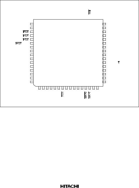
1.3Pin Arrangement
NC |
|
NC |
|
P22/TXD |
|
P21/RXD |
|
P20/SCK3 |
|
P87 |
|
P86 |
|
P85 |
|
P84/FTIOD |
|
P83/FTIOC |
|
P82/FTIOB |
|
P81/FTIOA |
|
P80/FTCI |
|
|
|
NC |
|
NC |
|
|
|
|
|
|
|
|
|
|
|
|
|
|
|
|
|
|
|
|
|
|
|
|
|
|
|
|
|
|
|
|
|
|
|
|
|
|
|
|
|
|
|
|
|
|
|
|
|
|
|
|
|
|
|
|
|
|
|
|
|
|
|
|
48 47 46 45 |
44 43 42 41 40 39 38 37 36 35 34 33 |
32 |
||||||||
|
NC |
49 |
|
|
|
|
|
|
|
|
|
|
|
NC |
50 |
|
|
|
|
|
|
|
|
|
31 |
|
P14/ |
51 |
|
|
|
|
|
|
|
|
|
30 |
|
P15/ |
52 |
|
|
|
|
|
|
|
|
|
29 |
|
P16/ |
53 |
|
|
|
|
|
|
|
|
|
28 |
P17/ |
/TRGV |
54 |
|
|
|
|
|
|
|
|
|
27 |
|
PB4/AN4 |
55 |
|
|
|
|
|
|
|
|
|
26 |
|
PB5/AN5 |
56 |
|
|
|
|
|
H8/3694 Series |
25 |
|||
|
|
57 |
|
|
|
|
|
24 |
||||
|
PB6/AN6 |
|
|
|
|
|
Top view |
|
||||
|
|
58 |
|
|
|
|
|
|
23 |
|||
|
PB7/AN7 |
|
|
|
|
|
|
|
|
|
||
|
PB3/AN3 |
59 |
|
|
|
|
|
|
|
|
|
22 |
|
PB2/AN2 |
60 |
|
|
|
|
|
|
|
|
|
21 |
|
PB1/AN1 |
61 |
|
|
|
|
|
|
|
|
|
20 |
|
PB0/AN0 |
62 |
|
|
|
|
|
|
|
|
|
19 |
|
NC |
63 |
|
|
|
|
|
|
|
|
|
18 |
|
NC |
64 |
|
|
|
|
|
|
|
|
|
17 |
|
|
1 |
2 |
3 |
4 |
5 |
6 |
7 |
8 |
9 |
10 11 12 13 14 15 16 |
|
NC
NC
P76/TMOV
P75/TMCIV
P74/TMRIV
P57/SCL
P56/SDA
P12
P11
P10/TMOW
P55/
 /
/

 P54/
P54/

P53/
 P52/
P52/

NC
NC
NC NC |
AV |
X2 |
X1 |
V |
TEST |
V |
OSC2 |
OSC1 |
V |
NC |
NC |
|
CC |
|
|
CL |
|
SS |
|
|
CC |
|
|
Note: Do not connect NC pins. |
|
|
|
|
|
|
|
|
P50/ |
P51/ |
|
|
|
|
|
|
|
|
|
|
|
|
Figure 1-2 Pin Arrangement of H8/3694 Series of the F-ZTATTM and Mask-ROM Versions
(FP-64E, FP-64A)
Rev. 1.0, 07/01, page 3 of 372
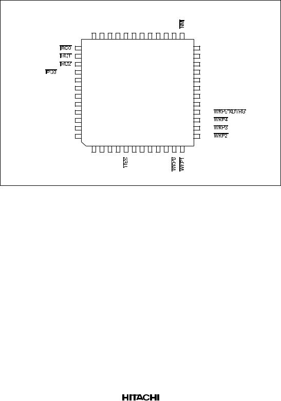
|
|
P22/TXD |
P21/RXD |
P20/SCK3 |
P87 |
P86 |
P85 |
P84/FTIOD |
P83/FTIOC |
P82/FTIOB |
P81/FTIOA |
P80/FTCI |
|
|
|
|
|
36 |
35 |
34 33 |
32 |
31 30 29 |
28 |
27 26 |
25 |
P76/TMOV |
|||||
|
P14/ |
37 |
|
|
|
|
|
|
|
|
|
|
24 |
||
|
P15/ |
38 |
|
|
|
|
|
|
|
|
|
|
23 |
P75/TMCIV |
|
|
P16/ |
39 |
|
|
|
|
|
|
|
|
|
|
22 |
P74/TMRIV |
|
P17/ |
/TRGV |
40 |
|
|
|
|
|
|
|
|
|
|
21 |
P57/SCL |
|
|
PB4/AN4 |
41 |
|
|
|
|
|
|
|
|
|
|
20 |
P56/SDA |
|
|
PB5/AN5 |
42 |
|
|
|
|
|
|
|
|
|
|
19 |
P12 |
|
|
PB6/AN6 |
43 |
|
|
H8/3694 Series |
|
|
|
18 |
P11 |
|
||||
|
PB7/AN7 |
44 |
|
|
|
Top View |
|
|
|
|
17 |
P10/TMOW |
|||
|
PB3/AN3 |
45 |
|
|
|
|
|
|
|
|
|
|
16 |
P55/ |
/ |
|
PB2/AN2 |
46 |
|
|
|
|
|
|
|
|
|
|
15 |
P54/ |
|
|
PB1/AN1 |
47 |
|
|
|
|
|
|
|
|
|
|
14 |
P53/ |
|
|
PB0/AN0 |
48 |
|
|
|
|
|
|
|
|
|
|
13 |
P52/ |
|
|
|
1 |
2 |
3 |
4 |
5 |
6 |
7 |
8 |
9 |
10 11 12 |
|
|
||
|
|
AVcc |
X2 |
X1 |
VCL |
|
TEST |
VSS |
OSC2 |
OSC1 |
Vcc |
P50/ |
P51/ |
|
|
|
|
|
|
|
|
|
|
|
|
|
|
|
|
||
Figure 1-3 Pin Arrangement of H8/3694 Series of the F-ZTATTM and Mask-ROM Versions (FP-48F)
Rev. 1.0, 07/01, page 4 of 372

1.4Pin Functions
Table 1-1 Pin Functions
|
|
|
Pin No. |
|
|
|
Type |
Symbol |
FP-64E FP-48F |
I/O |
Functions |
||
|
|
FP-64A |
|
|
|
|
|
|
|
|
|
|
|
Power |
VCC |
12 |
10 |
Input |
Power supply pin. Connect this pin to the |
|
source |
|
|
|
|
system power supply. |
|
|
|
|
|
|
|
|
pins |
VSS |
9 |
7 |
Input |
Ground pin. Connect this pin to the system |
|
|
|
|
|
|
power supply(0V). |
|
|
|
|
|
|
|
|
|
AVCC |
3 |
1 |
Input |
Analog power supply pin for the A/D converter. |
|
|
|
|
|
|
When the A/D converter is not used, connect |
|
|
|
|
|
|
this pin to the system power supply. |
|
|
|
|
|
|
|
|
|
VCL |
6 |
4 |
Input |
Internal step-down power supply pin. Connect |
|
|
|
|
|
|
a capacitor of around 0.1μF between this pin |
|
and the Vss pin for stabilization.
Clock OSC1 |
11 |
9 |
Input |
|
pins |
|
|
|
|
|
|
|
|
|
|
OSC2 |
10 |
8 |
Output |
These pins connect with crystal or ceramic oscillator for the system clock, or can be used to input an external clock.
See section 5, Clock Pulse Generators, for a typical connection.
|
X1 |
5 |
3 |
Input |
These pins connect with a 32.768 kHz crystal |
|
|
|
|
|
oscillator for the subclock. See section 5, Clock |
|
X2 |
4 |
2 |
Output |
|
|
Pulse Generators, for a typical connection. |
||||
|
|
|
|
|
|
|
|
|
|
|
|
System |
RES |
7 |
5 |
Input |
Reset pin. When this driven low, the chip is |
control |
|
|
|
|
reset. |
|
|
|
|
|
|
|
TEST |
8 |
6 |
Input |
Test pin. Connect this pin to Vss. |
|
|
|
|
|
|
Interrupt |
NMI |
35 |
25 |
Input |
Non-maskable interrupt request input pin. |
pins |
|
|
|
|
|
|
|
|
|
|
|
|
IRQ0 to |
51 to 54 |
37 to 40 |
Input |
External interrupt request input pins. Can |
|
IRQ3 |
|
|
|
select the rising or falling edge. |
|
|
|
|
|
|
|
WKP0 to |
13, 14, |
11 to 16 |
Input |
External interrupt request input pins. Can |
|
WKP5 |
19 to 22 |
|
|
select the rising or falling edge. |
|
|
|
|
|
|
Timer A |
TMOW |
23 |
17 |
Output |
This is an output pin for divided clocks. |
|
|
|
|
|
|
Timer V |
TMOV |
30 |
24 |
Output |
This is an output pin for waveforms generated |
|
|
|
|
|
by the output compare function. |
|
|
|
|
|
|
|
TMCIV |
29 |
23 |
Input |
External event input pin. |
|
|
|
|
|
|
|
TMRIV |
28 |
22 |
Input |
Counter reset input pin. |
|
|
|
|
|
|
|
TRGV |
54 |
40 |
Input |
Counter start trigger input pin. |
|
|
|
|
|
|
Rev. 1.0, 07/01, page 5 of 372

|
|
Pin No. |
|
|
||
Type |
Symbol |
FP-64E |
FP-48F |
I/O |
Functions |
|
|
|
FP-64A |
|
|
|
|
|
|
|
|
|
|
|
Timer W |
FTCI |
36 |
26 |
Input |
External event input pin. |
|
|
|
|
|
|
|
|
|
FTIOA to |
37 to 40 |
27 to 30 |
I/O |
Output compare output/ input capture input/ |
|
|
FTIOD |
|
|
|
PWM output pin |
|
|
|
|
|
|
|
|
I2C bus |
SDA |
26 |
20 |
I/O |
IIC data I/O pin. Can directly drive a bus by |
|
inerface |
|
|
|
|
NMOS open-drain output. |
|
|
|
|
|
|
|
|
(IIC) |
SCL |
27 |
21 |
I/O |
IIC clock I/O pin. Can directly drive a bus by |
|
|
|
|
|
|
NMOS open-drain output. |
|
|
|
|
|
|
|
|
Serial |
TXD |
46 |
36 |
Output |
Transmit data output pin |
|
communi- |
|
|
|
|
|
|
cation |
|
|
|
|
|
|
interface |
|
|
|
|
|
|
RXD |
45 |
35 |
Input |
Receive data input pin |
||
(SCI) |
||||||
|
|
|
|
|
||
|
|
|
|
|
|
|
|
SCK3 |
44 |
34 |
I/O |
Clock I/O pin |
|
|
|
|
|
|
|
|
A/D |
AN7 to |
55 to 62 |
41 to 48 |
Input |
Analog input pin |
|
converter |
AN0 |
|
|
|
|
|
|
|
|
|
|
|
|
|
ADTRG |
22 |
16 |
Input |
A/D converter trigger input pin. |
|
|
|
|
|
|
|
|
I/O ports |
PB7 to |
55 to 62 |
41 to 48 |
Input |
8-bit input port. |
|
|
PB0 |
|
|
|
|
|
|
|
|
|
|
|
|
|
P17 to |
51 to 54, |
37 to 40 |
I/O |
7-bit I/O port. |
|
|
P14, |
23 to 25 |
17 to 19 |
|
|
|
|
P12 to |
|
|
|
|
|
|
P10 |
|
|
|
|
|
|
|
|
|
|
|
|
|
P22 to |
44 to 46 |
34 to 36 |
I/O |
3-bit I/O port. |
|
|
P20 |
|
|
|
|
|
|
|
|
|
|
|
|
|
P57 to |
13, 14, |
20, 21, |
I/O |
8-bit I/O port |
|
|
P50 |
19 to 22, |
13 to 16, |
|
|
|
|
|
26, 27 |
11, 12 |
|
|
|
|
|
|
|
|
|
|
|
P76 to |
28 to 30 |
22 to 24 |
I/O |
3-bit I/O port |
|
|
P74 |
|
|
|
|
|
|
|
|
|
|
|
|
|
P87 to |
36 to 43 |
26 to 33 |
I/O |
8-bit I/O port. |
|
|
P80 |
|
|
|
|
|
|
|
|
|
|
|
|
Other |
NC |
1,2 |
|
|
These pins must be left unconnected. |
|
|
|
15 to 18 |
|
|
|
|
31 to 34
47 to 50 63, 64
Rev. 1.0, 07/01, page 6 of 372
Loading...