

CAUTION Before servicing this chassis, it is important that the service technician reads the "Safety Precautions" and "Product Safety Notices" in this Service Manual.
CONTENTS
| SAFETY PRECAUTIONS 2 | HORIZONTAL CENTER POSITION ADJUSTMENT |
|---|---|
| PRODUCT SAFETY NOTICE | |
| SPECIFICATIONS | VERTICAL AMPLITUDE ADJUSTMENT 12 |
| ADJUSTMENT POINT 12 | |
| PENOTE CONTROL UNIT | BASIC CIRCUIT DIAGRAM 13 |
| PRINTED WIRING BOARD 16 | |
| WAVEFORMS | |
| WIRING DIAGRAM | |
| REPLACEMENT PARTS LIST 19 | |
| AGC ADJUST MENT |
SPECIFICATIONS AND PARTS ARE SUBJECT TO CHANGE FOR IMPROVEMENT
COLOR TELEVISION
JUNE 1997
Fujian Hitachi Television Co., Ltd.
CMT1473/1471
WARNING. The following precautions should be ob-
- 1. Do not install, remove, or handle the picture tube in' away from the body while handing
- 2. When service is required, an isolation transformer should be inserted between power line and the receiver before any service is performed on the chas-
- 3 When replacing the chassis in the cabinet ensure all the protective devices are put back in place, such as barriers non-metallic knobs adjustment or compartment covers or shields, isolation resistors/capacitors,
- 4. When service is required, observe the original lead dressing. Extra precaution should be taken to assure area. Particularly note the R. G. B. lead dressing. Ensure they are dressed well away from the horizontal scan and F. B. T. circuitry.
- 5. Always use the manufacturer's replacement component. Always replace original spacers and mintain lead lengths. Especially critical components are indicated thus A on the parts list and should not be re-
- place those components that indicate evidence of overheating.
- 6. Before returning a serviced receiver to the cusoperate without danger of electrical shock and he sure that no protective device built into the instrument by the manufacturer has become defective, or inadvertently damaged during servicing. Therefore, the following checks are recommended for the continued protection of the customers and service technicians.
Insulation resistance should not be less than 7MO at 500V DC between the mains poles and any accessible metal parts. Also, no flashover or breakdown should
neles and accessible metal narts
could produce X-radiation moderately in excess of design levels. The high voltage must not under any circumstances exceed 28 5 kW on the short-Y-RADIATION
TUBES. The primary source of X-radiation in this receiver is the picture tube. The tube utilised for the above mentioned function in this chassis is specially constructed to limit X-radiation For continued X-radiation protection, replace tube with
the same type as the original HITACHI approved type PRODUCT SAFETY NOTICE
Many electrical and mechanical parts in HITACHI television receivers have special safety telated characteristics. These characteristics are often not evident from visual inspection, nor can the protection afforded by them necessarily be obtained by using replacement components rated for higher voltage, wattage, etc. Replacement parts which have these special safety chatacteristics are identified by marking with a A on the schematics and replacement parts list in this Service nent which does not have the same safety characteristics as the HITACHI recommended teplacement one. Product Safety is continuously under review, and new information, always consult the current HITACHI Service Manual, A subscription to or additional copies of HITACHI Service Manuals, may be obtained at a nominal charge from your HITACHI SALES OFFICES TUBE DISCHARGE
The line output stage can develop voltages in excess of
| CPT1470 | SPECIFICA | TIONS | ||
|---|---|---|---|---|
| RF | B. G/PAL | Aerial input | 75Ω unbalanced type | |
| VIDEO | NTSC 50 | Color picture tube | A34KPU02XX/A 34JQQ90X03 | |
| Reception system |
NTSC3. 58
NTSC4. 43 PAL60 |
Speaker | 9cm×5cm | |
| Sound Output | 3w | |||
| Power supply | AC240V(50Hz) | |||
| CCIR: E2~12,E21~69,S01~3, | Power consumption | 66w | ||
| Channel coverage | Australia | S1~10,S11~20,S21~41 | Weight(kg) | 10 |
| 28~69 |
Dimensions
W×H×D(cm) |
37. 6×33. 7×37. 7 | ||
PT1470
PECIFICATIONS CMT1473
| 625-lines B. G/I/D. K/H PAL | B. G/I/D. K/H PAL | Aerial input | 750 unbalanced type | |
|---|---|---|---|---|
| Reception system |
B. G/D. A/K1 SECAM
NTSC50 525-lines M/NTSC NTSC 3. 58-5. 5/6. 0/6. 5 NTSC 4. 43-5. 5/6. 0/6. 5 |
Color picture tube | A34KPU02XX/A34JQQ90X03 | |
| Roopton of our | Speaker | 9cm×5cm | ||
| Sound Output | 3W | |||
| FAL UU | Power supply | AC110-230V(50/60Hz) | ||
|
CCIR:
E2~12,E21~69,S01~3,
S1~10,S11~20,S21~41 OIRT: R1~12,R21~69 JAPAN: J1~12,J13~62 U.S. A.: US2~13,J~W,US14~69 Hong Kong, U.K.; UK21~69 CHINA, CIAT2 C1~22,C13~57 |
Power consumption | 65w | ||
| Channel coverage | Weight(kg) | 10 | ||
|
Dimensions
W×H×D(cm) |
37. 6×33. 7×37. 7 | |||
SPECIFICATIONS CMT1471 B. G/D. K/K1 SECAM A34KPU02XX/A34JQQ90X03 Reception system 525-lines NTSC3, 58(VIDEO) 9cm×5cm Power supply E2~12.E21~69.S01~3. OIRT R1~12,R21~69 Hong Kong, U. K. : UK21~69 CHINA: C1~12.C13~57 37.6×33.7×37.7
* Specifications are subject to change without notice to improve performance.
_ 3 _
CONTROLS
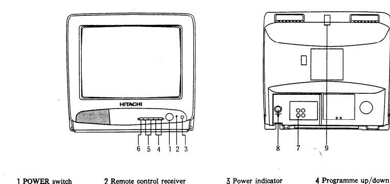
OMT1479 /1471
6 TV/VIDEO selection
DEMOTE CONTROL UNIT
CIPCUIT DESCRIPTION
Tuner and I. F. Stages
Sound I. F. Stages
cuitry of the 1C
Vision I. F. Stages .
in Table 1. But CP202 is only used for CMT1473.
demodulator, and IC4501, which is the output ampli-
The I.F. signal at the collector of O201, is fed via fil-
The composite signal output from pin 7 of IC201 is in-
nut to around filters ME401 ME402 ME403 and
ME404 and selected with the mode shown in Table 1
at IC451 after being output from the filter. The select-
sound output being obtained from pin 50. It is then input to pin 5 of IC4501 via C408, for further amplifica-
Volume control is performed by the DC voltage applied
to pin 5 of IC201. This is obtained via R427 from pin 8 of IC1101. Sound demodulation output at pin 1 of IC201, is applied to the terminal of rear via Q401.
Audio signals from external equipment can be applied
to the input terminal of tear. They are then input to
IC201 at pin 6. When connecting audio signals this way, a "High" is applied to pins 16 of IC201 from
IC1101, thereby changing the internal switching cir-
B·G/D·K M/I Saw filter Sound filter Sound trap
The 1 E signal from CP201 and CP202 is input to pins
trolled by the AGC circuit. The response speed of this
MEA02/5 EMIL
MF404(6.5MHz)
CP202 ME401(4, 5MHz) ME503
(IC451 is not used for CDT1470 )
ter CP201 or CP202 and input to IC201 at pins 45 and
internal AGC stage is determined by the external components connected to pin 48.
The tuner used on this chassis, is powered by the + 9V. supply, and covers VHF, UHF and CATV Hyper The output from the L.F. amplifier is then fed to the video detector circuritry. The picture carrier is limited Band The L E output from the tuner is applied to amplifier O201 then input to CP201 of CP202 as shown connected between pins 2 and 3 of the IC. This pro-The sound stages consist of IC201, which is basically a
An RF AGC voltage is made available at pin 48 of IC201, the starting level of which is determined by the voltage applied to pin 49, which in turn is fixed by the setting of VR202 This AGC voltage is then fed to the tuner via R208 to control its gain accordingly. The composite video finally emerges at pin 7 of IC201.
Luminance Circuitry
The composite video signal output from pin 7 of IC201 is applied to the sound rejection filter MF501, MF502, and ME503 But ME502 and ME503 are not used for CPT1470
The resulting luminance signal is applied to the terminal of rear.for output to external equipment if desired. It is then returned to pin 13 of IC201 via Q506, for colour decoding and deflection synchronisation The luminance signal is added internally to the R. G. B. matrix circuits of IC201, as well as being controlled
The voltages to control the contrast and brightness levels are output from pins 3 and 4 of IC1101, then applied to pins 17 and 25 of IC201.
chassis Should the beam current start to tise, the voltfall is applied to the cathode of D758, then via R760 to
pin 25 of IC201, thereby reducing the contrast level
terminal of teat, ate fed to IC201 pin 15.
When the external mode is selected a "High" is applied to pin 16 of IC201.
Chrominance Circuitry
IC201 is designed to demodulate PAL, NTSC and SE-CAM systems
And this IC can distinguish between PAL. NTSC of SE-
nals, then fed to pins 14 and 16 of IC501 which is a

MEEDI
MF502
CMT1273/147
IC201 allows bi-directional communication between the SECAM decoder IC502 and automatic system manager for SECAM identification. It delivers the VCXO (voltage controlled xtal osillator ) reference frequency (1 (3)MHz only) to the SECAM decoder via pin 32 of IC201. Once SECAM is identified, the gated reference signal is outputted to pin 32 of IC201
The inputs at pins 14 and 16 are clamped then fed via a buffer stage to internal delay lines, which are driven by a clock signal of 3MHz to obtain a delay period of 641 Seconds. This internal clock is generated from a 6MHz voltage controlled oscillator, and line locked by the sandcastle pulse input at pin 5. Low pass filters af-The undelayed and the delayed signals are then added. with the resulting R-v and B-v signals being output These supports are then fed to IC201 at pins 28 and 29
This 1C contains clamping circuits, and a DC colour saturation control, the level of which is set by the voltage applied to nin 26 from nin 5 of IC1101 The signals are then applied to a MATRIX circuit, and finally emerge from pins 18, 19 and 20 as the blue, green, and
IC501 and IC502 are not used for CPT1470. Deflection Circuits
The deflection circuitry of IC201 contains a sync, separator stage, horizontal oscillator and output stages, a
vertical count-down and output stage
Horizontal Stage -
The composite video signal from pin 7 of IC201 is returned to pip 13 via C302 as explained previously. This
input is applied to the internal sync. separator stages of
A internal phase detector stage is provided with a sawtooth waveform, generated from the line pulse input to the second states will then compare this saw tooth waveform to the sync. pulse. Any frequency drift
The components connected to nin 40 form a filter net-
work for the phase detector and VR701/connected to pin 39 provides manual phase control. The horizontal of line drive transistor 0721, T721 couples the output of O721 to the line output transistor O781 Both these trainsistors are nowered by the 95V supply A line rectified by D751, smoothed by C756 and provides approximately 170V to drive the output transistors
O851. O852. O853. Under certain fault conditions, i. or reduced value of the tuning capacitor C781, an excess of E. H. T. could be developed. To prevent this happening, the rectified voltage of D751 is fed via potential divider R757. R758, and applied to ZD751. the zenet will be exceeded and a voltage will be an plied to pin 35 of IC1101 via R1106. thereby shutting
This effectively applies a"Low" to Q954 base, turning the transistor off Consequently, 0953 will be turned off and the + 8V supply to IC201 is then removed. thereby shutting down the deflection stages of the IC. preventing further E. H. T. generation.
fault conditions, so this is prevented in the following
The II The summer to the herizontal output states is
Should the current rise, the voltage drop across R781 will increase, and a voltage will be appiled to the gate of 0955. This will then prevent further E. H. T. generation as described earlier.
A supply of +25V is required for IC681. This is ob-
The internal vertical sync. of IC201 is fed to a triggered vertical divider stage, which counts down the horizontal frequency to obtain the vertical frequency, tor circuit.
This also has the advantage that no external frequency
C601 at pin 42 of the 1C is used for ramp generation, and produces the required sawtooth output.
The vertical output from nin 43 of IC201 is annlied to and and ICG91 win P604 The components D601 and C605 determine the flyback generation time, and the vertical output to drive the deflection coils is made
R609, is added to the feedback from R607/C608 etc. and the result is applied to pin 41 of IC201. The values of R607 and C608 determine the linearity, whilst VR 601 sets the vertical height.
Power Supply Circuit (1)Starting operation
• Power switch S901 turned ON→Rectified at D901~D904→Voltage at Q903 base rises→
P2)of T901-Drive voltage-Provide to Q905 of winding (B1-B2) of T901 -> O905 supply stable drive current to O903 base-> come into
(2) Switching constant voltage operation
• AC input voltage rises of + B load decreased (picture gets dark)→+B(95V)rises→Ic increased at 0951 → Id increased at IC901 → Ic increased at IC901 - Voltage decreased at nin (5) of IC901→ON period of O901 increased→ ON period of O903 decreased → Positive voltage of D951 anode decreased -> + B voltage age of LISSI anone decreased
(3)Standby operation • Remote control power OFF-IC110120and 2
₹→0954 OFF→0953 OFF→IC201 H. Start Pin (3) stopped-Horizontal deflection stopped. * Also > 0957 OFF > R965 connect into R964-
O903 is slightly decreased by IC901 -> + B voltage falls (about 62V) -> Power consumption decreased. + 5V power provided from TQ01 (S3-S4) winding through DQ52 and C954→5V at nin m of IC1101 stabilized by ZD1101
Remote Control and Tuning Circuitry:
The remote control receiving unit CP1201.contains an infrared amplifier and powered by the +5V supply. which is stabilized by 2D1101. The output from nin 9 of this unit is applied to pin 16 of IC1101.
This 1C type M37210M4, performs channel selection. UP/DOWN analogue control, an screen display, search tuning, and controls inputs and search tuning, and controls inputs and outputs to and from the AV terminal. IC1102 is the memory IC, which stores the data relating to the above functions, then transfers that information to IC1101 when required. Both these 1Cs are powered by the +5V supply. X1101 supplies IC1101 with a basic clock frequency which controls all operation a basic clock nego
When the TV is first switched on IC1101 must be initially reset, and this is achieved by IC1101 stage. As the +5V supply begins to rise from switch on pin 3 of oll 05 in held "Low" This is applied to pin 30 of IC1101 thus resetting the 1C. Once pin 1 of Q1105 has almost reached its + 5V potential, the "Low" is removed from nin 3 thus releasing the reset condition. When the search routine has been initiated and a signal has been located pin 14 of IC201 will become "High". This is applied to pin 34 of IC1101, and informs the IC that a signal is present. The search routine then stops,
and the IC will monitor the AFC signal present at pin
Pins 46 and 47 control the signal system. Contrast, colour, brightness, sharpness, tint, and volume are all controlled from the remote control handset (the volume can also be adjusted by + and - buttons on the front of the TV), and will produce DC level changes from pins 3~8 of IC1101. which are then fed to the relevant pins of IC201.
Pins 31~32.37~39 and 11 from the in and out ma-
Ding 12 and 13 are the clock and data output Dins. These signals are supplied to the memory IC1102. It is supplied to pin 16 of IC201. When "High", the IC will process external inputs applied to pins 6 and 15. and when "Low", the internal signals are processed.
The handset button marked TV/VIDEO will need to be pressed. This will then produce the required "High"
million outputs. sustaint from pine 50, 51 and 52. The components
L1102, C1102, and C1103, on pins 28 and 29, determine the display oscillator frequency. The horizontal and vertical inputs at pins 1 and 2 determine the actual position of the on screen display. When a command requiring an on-screen display is received by IC1101.a
This is applied to pin 21 of IC201, and blanks out a nortion of the picture. The on-screen display informastar is then incontrol into this portion, thus resulting in a
clear display. When the ALARM mode has been set. and the time input has elapsed, an output is obtained
This is then applied via R1184.R1119.C1111.R1118 etc. to pin 5 of IC4501 thus causing a "Bleen"sound to be heard
Once the "OFF" timer mode has been set, and the time input has clapsed, pins 21 and 22 of IC1101 output a
This removes the supply to the base of O954 and as a result the +9V output of O953 disappears. This places
the TV into its standby mode of operation by removing E. H. T. generation as explained previously.
When the "ON" time has been estimated and set, the standby command must be transmitted by the handset. to place the TV into its standby mode. As an indication that the standby mode is only remporary, pin 36 of IC1101 is taken "High" and "Low" alternately, caus
When the entered time has elapsed, the "Low" outputs from pins 21 and 22 of IC1101 are removed and the TV will return to normal operation.
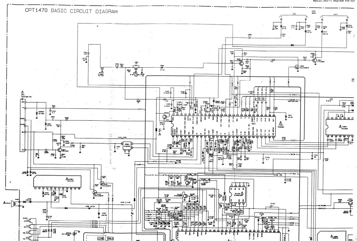
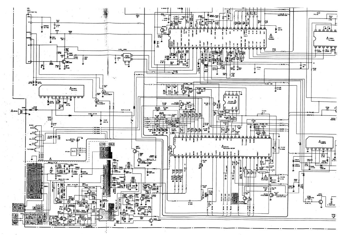
CPT1470
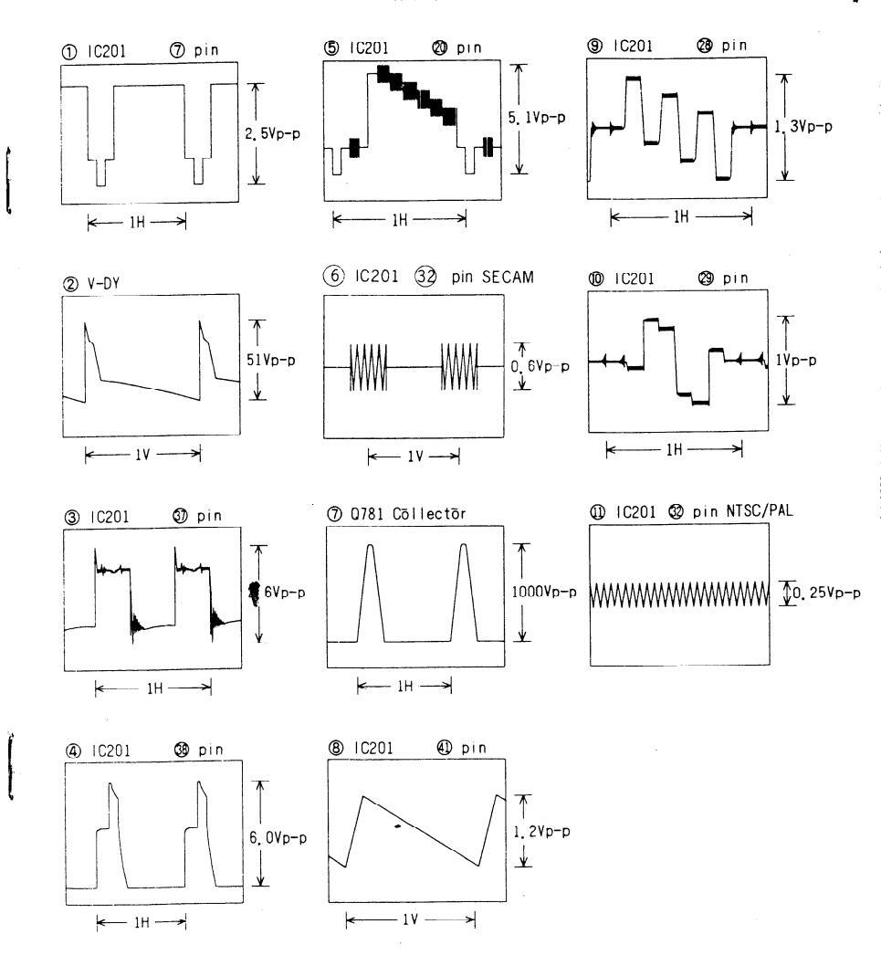
CPT1470 CMT1473/1471 PIN DESCRIPTION FOR IC201-TDA 8362 PIN NO. Audio deemphasis and +/- mod. switch Audio output of non-volume controlled and have to be buffered. Adjust AFC output voltage of 4. 3V measure at pin 44. Video identification output-N. C. Sound IF in plus volume control External audio input-Video output Decoupling digital supply Ground Positive supply (8V) Decoupling filter tuning Derived from internal RF video output (Pin 7) and supplied to the synchronization, lumine 2Vpk-pk)by selection. Peaking control input Derived from external video source and supplied to the synchroniza-tion, laminance and chrominance processing (level ≈ 1Vpk-pk) by se-External CVBS input DC voltage control the selection of internal/external CVBS(Pin 13 or 15)and audio. i. e. <0. 5V. Internal signals >7. 5V. External signals Brightness control input G-output RGB-insertion and blanking input R input for insertion B-input for insertion Color decoder selection between NTSC or PAL/SECAM. i. e. 0-5V:NTSC decoder activated >6V. PAL/SECAM decoder applied Hue control input R-Y Input signal R-Y output signal B-Y output signal SECAM Reference/Communication Loop filter burst phase detect 3. 58MHz X-tal connection Start supply pin. If the start voltage is below 5.8V, the horizontal Start horizontal oscillator output will be disabled. (Normal-7. 2V-8. 8V) Flyback input/sandcastle output Ø-1 loop filter Vertical feedback input Generates a linear sawtooth output for the vertical output stage This pin is the current output of the vertical pre-amplifier and drives the vertical deflection stage. Vertical drive output the vertical deflection stage. The amplifier has a feedback output. Pin 41, in order to serve the ine amplifier has a feedbac current in the vertical D. V. AFC outpu IF input from Tuner and Saw Filter. IF-input It input from 1 difer and 5aW fifter. Voltage to change the Tuner gain when RF input signal amplitude be-Tuner AGC output AGC decoupling capacitor The Tuner AGC control takes over when IF input reach input level. The take over point is adjusted at this point. Tuner take-over adjustmen Audio output Decoupling sound demodulator Decoupling bandgap supply
PIN DESCRIPTION FOR IC1101-M37210M4-655SP/657SP DESCRIPTION This is the horizontal synchronous signal input pin for On-screen display Input Input This is the horizontal synchronous signal input pin for On-screen disp. This is the vertical synchronous signal input pin for On-screen display Output Output of the different DC levels to control each function Output e. g. COLOR UP/DOWN, VOLUME UP/DOWN etc... Output Return of front control matrix Memory IC data IN/OUT Output Tuning control voltage to tuner AFS voltage input. After A/D conversion, this pin also serve to detect the AFC Input present of RF signal Remote con. serial data input from R/C receiving unit CP1201 Input To identify the frequency of RF signal. (50 Hz or 60 Hz) ON VHF L VHF H UHF BAND 1 BAND 2 23 CNVss GND OV 4 MHz Clock Out +5V Power supply +10% Tolerance. Display oscillator frequency our Display oscillator frequency input Resets When power is "ON" Input Color identification of SECAM NTSC or PAI Input A/D terminal served to detect the present of Hsync signal EEPROM chip select In/out EEPROM cmp select Output Output for front nanel control matrix to control vol. , programme... Output "High" when 4. 5MHz sound detected SKEW HITACHI DISPLAY High "HITACHI" display appears when no signal received Ident by pin 18 and controls output from this pin. 50Hz=L 60Hz=H Output In/Ou Output No connection Alarm output L=OFF Alarm _____ 50% Duty cycle Selects the sound system 4. 5HMz 5. 5MHz 6. 0MHz 6. 5MHz L In/Out I/M H BG/D.K H In/Ou 48 IDENT Output On-Screen-Display blanking output Blue output for On-Screen-Display
— 9 —
| CPT1470 | |
|---|---|
| CMT1473/1471 |
P. I. F. CARRIER FILTER ADJUSTMENT
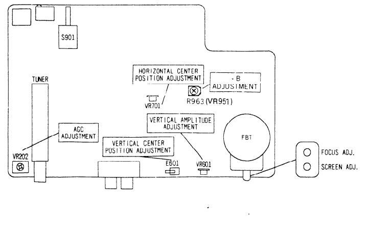
ADJUSTMENT LOCATION L202
| Preparations for adjustment | Adjustme | ent Procedure | Remarks/Waveform | |
|---|---|---|---|---|
| (1) |
Apply the following signal across IF
out and GND of tuner. VIDEO SIGNAL GENERATOR FP SIGNAL GENERATOR FP=38. 9Hz 2200P 50Ω FP=38. 9Hz 2200P FP=38. 9Hz 50Ω SIGNAL LEVEL :-10~0dBm SIGNAL :PHILIPS PATERN Connect the oscilloscope to the pin 40 of IC201. |
(1) Adjust L202
charge" is seen Then adjust L2 voltmeter as b |
until a "Fast rate of
non voltmeter. 202 to obtain reading on elow. . S±0.2V |
|
|
Delay
iC201 (7.6V) ♥ 33Ω Delay time →*8V Delay time ↓*8V |
+B ADJUSTMENT
ADJUSTMENT LOCATION R963 (VR 951)
| Treparations for adjustment | Adjustment Procedure | Remarks/Waveform | ||
|---|---|---|---|---|
| (1) | AC input voltage 220±5V/50Hz | (1) |
Adjust R963 (VR 951) to obtain
+B voltage as below: |
|
| (2) |
Turns on the set and set the brightness
and contrast to max. (SIGNAL:PHILIPS PATTERN) |
+B voltage=95±0.3V | ||
| (3) |
After 30 sec heat-run, check &
adjust the +B voltage. Measuring Point : +B voltage: C956-side GND : C956-side |
AGC ADJUSTMENT
ADJUSTMENT LOCATION VR202
| Preparations for adjustment | Adjustment Procedure | Remarks | ||
|---|---|---|---|---|
| 1 |
With the signal received, apply heat
run for more than two minutes to avoid the influence of circuit tempere- |
1 | Received following channel and strength. | |
| ture drift. |
CHANNEL;CCIR 5
STRENGTH; - 49dBm |
|||
| 2 | Connect the voltmeter of at least 100kΩ internal impedance to the AGC terminal of the tuner. | 2 |
Adjust VR202 until the following voltage is reached.
V1-(0.5v±0.2v) V1:the voltage without signal |
|
HORIZONTAL CENTER POSITION ADJUSTMENT
ADJUSTMENT LOCATION VR701
- 11 -
VERTICAL AMPLITUDE ADJUSTMENT
ADJUSTMENT LOCATION VR601
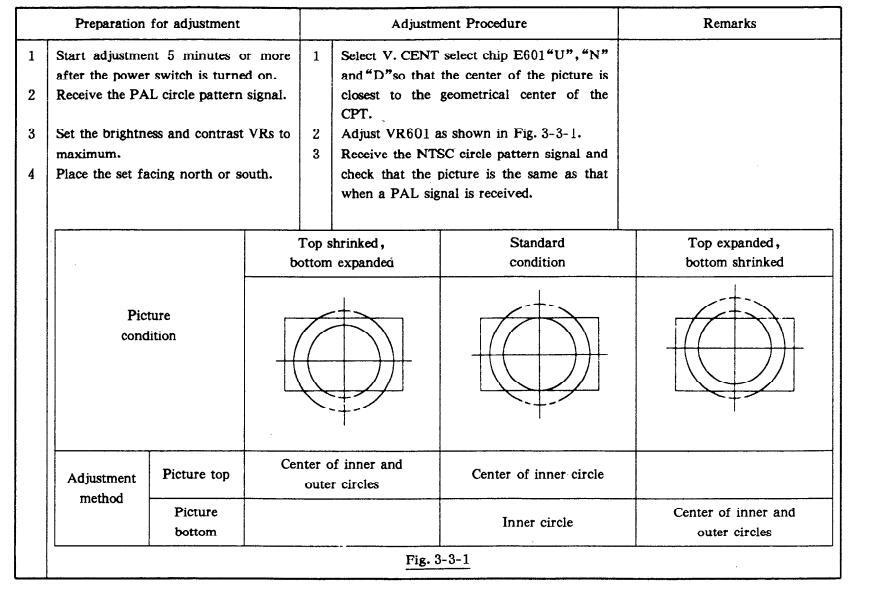

- 12-
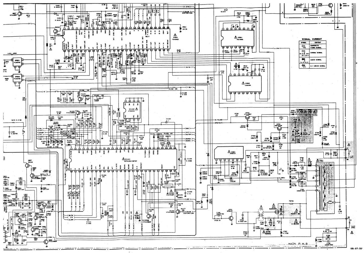
PRODUCT SAFETY NOTE Componer safety.Before replacing any c
• Since this is a basic c: • ALL DC voltage to bé me ·Voltage taken on a com
PRODUCT SAFETY NOTE: Components marked with a and shaded have special characteristics important to safety. Before replacing any of these components, read carefully the PRODUCT SAFETY NOTICE of this Service Manual. Don't degrade the safety of the receiver through improper servicing.

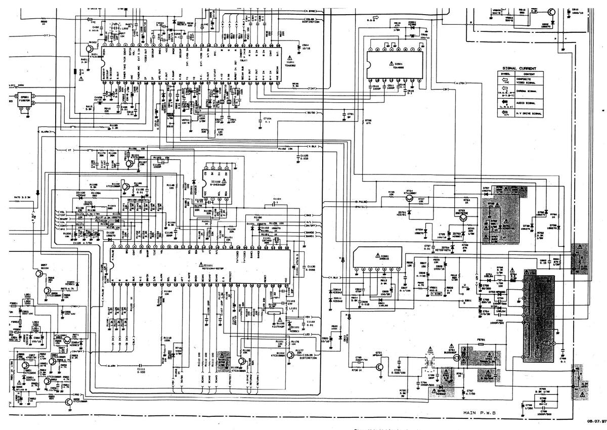
• Since this is a basic circuit diagram, the value of the parts subject is to be altered for improvement. • ALL DC voltage to be measured with a tester(100KQ/v).
Voltage taken on a complex color bar signal including a standard color bar signal.
-13-
PRODUCT SAFETY NOTE: C safety.Before replacin
Manual.Don't degrade

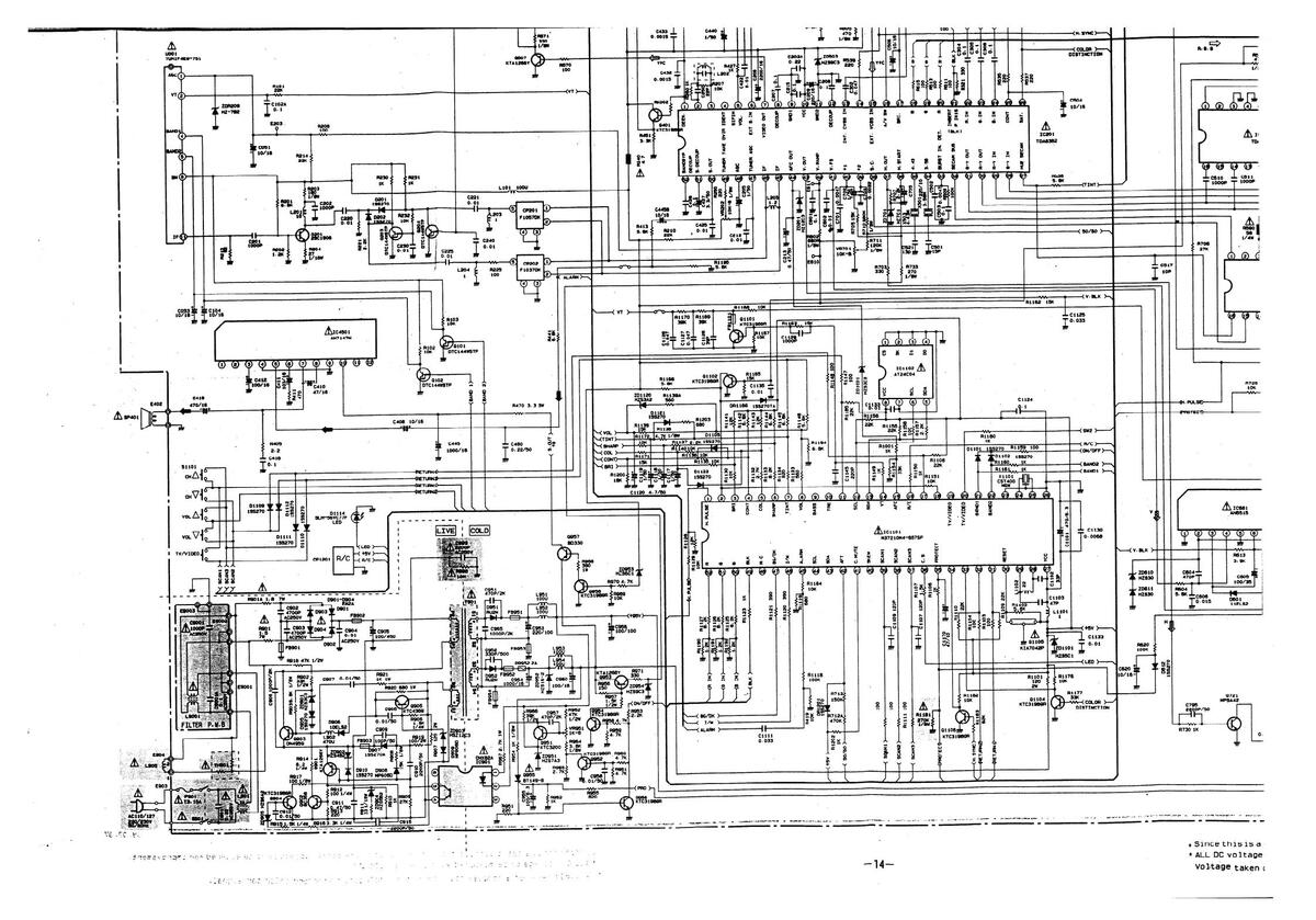
PRODUCT SAFETY NOTE: Components marked with and shaded have special characteristics important to safety. Before replacing any of these components, read carefully the PRODUCT SAFETY NOTICE of this Service

. Since this is a basic circuit diagram, the value of the parts subject is to be altered for improvement. • ALL DC voltage to be measured with a tester(100KΩ/v).
Voltage taken on a complex color bar signal including a standard color bar signal.
111 2018년 1월 2018년 1월 2010년 1월 2011년 1 1월 28년 1월 2011년 1월 20
-14-
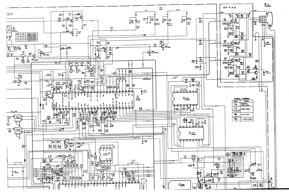
PRODUCT SAFETY NOTE: safety.Before replaci
Since this is a b. ALL DC voltage t Voltage taken or
• Since this is a basic circuit diagram, the value of the parts subject is to be altered for improvement. • ALL DC voltage to be measured with a tester(100KQ /v).
PRODUCT SAFETY NOTE: Components marked with and shaded have special characteristics important to safety. Before replacing any of these components, read carefully the PRODUCT SAFETY NOTICE of this Service
Manual Don't degrade the safety of the receiver through improper servicing

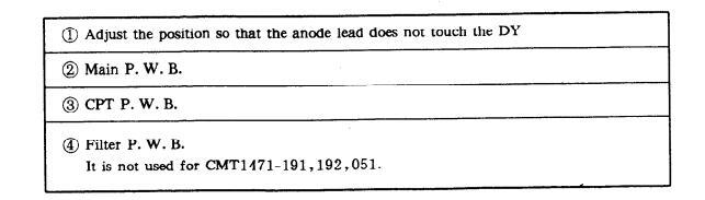
MAIN P. W. B.
......................................
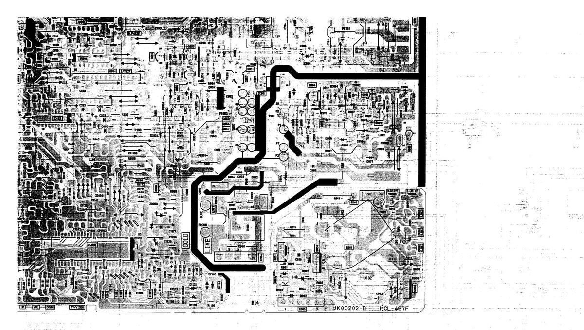
FILTER P. W. B.

WAVEFORMS
CPT1470 CMT1473/1471 WIRING DIAGRAM FE992 ⊏ E991 FOCUS E805 6
REPLACEMENT PARTS LIST
PRODUCT SAFETY NOTE ; Components marked with a A have special characteristics important to safety. Before replacing any of these components, read carefully the PRODUCT SAFETY NOTICE of this Service Manual, Don't degrade the safety of the receiver through improper servicing.
| ABBREVIATIONS : | CapacitorsCD: Ceramic disk, PF: Polyester Film, EL: Electrolytic, PP: Polypropylene, |
|---|---|
| PR: Paper, TA: Tantalum, TM; Trimmer. | |
| Resistors CF: Carbon film, WW: Wire wound, FR: Fuse Resistor, MG: Metal Glazed, | |
| VR: Variable Resistor, CC: Carbon Composition, MF: Metal Oxide Film. | |
| SemiconductorsTR: Transistor, DI: Diode, ZD: Zener Diode, VA: Varistor, TH: Thermistor |
| SYMBOL | DART NO | DESCRIPTION | SYMBOL | PART NO | DESCRIPTION |
|---|---|---|---|---|---|
| NO. | PARI NU. | DESCRETION | NO. | i fatt het | |
| C051 | 0800015RA | EL 10MF 16V | C225 | 0880009R | PF0. 01 MF +−10%50V(1473) |
| C053 | 0800015RA | EL 10MF 16V | C230 | 0880009 R | PF0. 01MF+-10%50V(1473) |
| C101 | 0800048RA | EL 100MF 10V | C231 | 0800048RA | EL 100MF 10V |
| C102 | 0880016R | PF0. 1MF+−10% 50V | C240 | 0880009 R | PF0. 01MF+−10% 50V(1473) |
| C102A | 0880016R | PF0. 1MF+-10%50V | C250 | 0890118R | CD 22PF+-5%50V |
| C103 | 0880009R | PF0. 01MF+-10%50V | C251 | 0880003R | PF 1000 PF +−10% 50 V |
| C104 | 0800015RA | EL10MF 16V | C302 | 0880014R | PF0. 047MF+−10% 50V |
| C1101 | 0800072RA | EL 470MF6. 3V | C304 | 0880016R | PF0. 1 MF +−10% 50 V |
| C1102 | 0890067R | CD 33PF+-5%50V | C305 | 0880016R | PF0. 1 MF +−10% 50 V |
| C1103 | 0890069R | CD47PF+-5%50V | C306 | 0880016R | PF0. 1MF+−10% 50V |
| C1107 | 0890075R | CD120PF+ 5%50V | C310 | 0800015RA | EL 10MF 16V |
| C1108 | 0890075R | CD120PF+-5%50V | C311 | 0800015RA | EL 10MF 16V(1473) |
| C1109 | 0890075 R | CD120PF+-5%50V | C311A | 0800015RA | EL 10MF 16V |
| C1111 | 0880013R | PF0. 033MF+−10%50V | C312 | 0800015RA | EL 10MF 16V |
| C1117 | 0800003RA | EL 1MF 50V | C313 | 0800048RA | EL 100MF 10V |
| C1118 | 0800003RA | EL 1MF 50V | C350 | 0880009R | PF0. 01MF+-10% 50V(1473) |
| C1119 | 0800003RA | EL 1MF 50V | C351 | 0244171 RA | CD 0.01MF 50V |
| C1120 | 0800012RA | EL 4. 7MF 50V | C40.1 | 0880003R | PF 1000PF+−10% 50V |
| C1124 | 0880016R | PF 0. 1MF+−10% 50V | C402 | 0880009R | PF0. 01MF+-10% 50V |
| C1125 | 0880013R | PF0. 033MF+-10%50V | C408 | 0800015RA | EL 10MF 16V |
| C1126 | 0890122R | CD 39PF+-5%50V | C410 | 0800041RA | EL 47MF 16V |
| C1127 | 0880014R | PF0. 047MF+-10%50V | C411 | 0800049RA | EL 100MF 16V |
| C1128 | 0880014R | PF0. 04MF+-10%50V | C412 | 0800049RA | EL 100MF 16V |
| C1129 | 0880003R | PF1000PF+-10%50V | C416 | 0880016 R | PF 0.1MF +−10%50 V |
| C1130 | 0880008R | PF6800PF+-10%50V | C418 | 0800074NA | EL 470MF 16V |
| C1133 | 0880009R | PF0.01MF+-10%50V | C422 | 0880009R | PF0. 01MF+-10%50V |
| C1135 | 0880009R | PF0. 01MF+-10%50V | C425 | 0880009R | PF0. 01MF+-10%50V |
| C1145 | 0890078R | CD220PF+-5%50V | C427 | 0800007RA | EL 3. 3MF 50V |
| C1170 | 0800039RA | EL47MF10V | C428 | 0880016R | PF0. 1 MF +−10% 50 V |
| C201 | 0890087R | CD 1000PF+-10% 50V | C432 | 0880004R | PF1500PF+−10% 50V |
| C202 | 0890087R | CD1000PF+-10%50V | C433 | 0880004R | PF1500PF+-10% 50V |
| C205 | 0800003RA | EL 1MF 50V | C440 | 0284623R | EL 1MF 50V(BP) |
| C206 | 0800087FA | EL 2200MF 16V | Č 441 | 0800041RA | EL 47MF 16V |
| C207 | 0880016R | PF0. 1MF+-10%50V | C445 | 0800082FA | EL 1000MF 16V |
| C208 | 0880016R | PF0. 1MF+-10%50V | C4501 | 0800015RA | EL 10MF 16V (1473) |
| C212 | 0880009R | PF0. 01MF+-10%50V | C458 | 0800015RA | EL 10MF 16V |
| C213 | 0800001RA | EL0. 47MF 50V | C501 | 0890116R | CD SL 15PF+-5%50V |
| C215 | 0880016R | PF0. 1MF+-10%50V | C502 | 0880007R | PF 4700PF+−10%50V |
| C220 | 0880009R | PF0. 01MF+-10%50V | C503 | 0880016R | PF0. 1MF+−10%50V |
| C221 | 0880009R | PF0.01MF+-10%50V(1473) | C504 | 0800015RA | EL 10MF 16V |
- 19 -
PRODUCT SAFETY NOTE : Components marked with a have special characteristics important to safety. Before replacing any of these components, read carefully the PRODUCT SAFETY NOTICE of this Service Manual. Don't degrade the safety of the receiver through improper servicing.
CPT1470
CMT1473/1471
| SYMBOL NO. | PART NO. | DESCRIPTION |
SYMBOL
NO. |
PART NO. | DESCRIPTION |
|---|---|---|---|---|---|
| C506 | 0800015R 4 | EL 10ME 16V | C801 | 0244113FA | CD330PF+-10%50V |
| C500 | 0800048R A | EL 100ME 10V | C802 | 0890082R | CD390PF+-10% 50V |
| C510 | 08900878 | CD 1000PF+-10% 50V | C803 | 0890083R | CD470PF+-10%50V |
| C511 | 0890087R | CD 1000PF + -10% 50V | C805 | 0245612F | CD4700PF+-10%1KV |
| C512 | 0800049RA | EL 100MF 16V (1473,1471) | C810 | 0800081RA | EL 1000MF 10V |
| C513 | 08800168 | PF0. 1MF+-10% 50V(1473.1471) | ∧C901 | 0262774 | PF0. 22MF 250V |
| C514 | 08800188 | PF0. 22MF+-10% 50V | C902 | 0248593F | CD4700PF+80-20%250V |
| 0014 | (1473.1471) | C903 | 0248593F | CD4700PF+80-20%250V | |
| C515 | 0880016R | PF0. 1MF+-10% 50V | C904 | 0248594F | CD0.01MF+80-20%250V |
| C516 | 0880016R | PF0. 1MF+-10%50V | C905 | AL00099 | EL100MF450V |
| C517 | 0890061R | CD 10PF+-5%50V | C906 | 0244211A | CD1000PF2KV |
| C521 | 0248663RA | CD SL 13PF+-5%50V | C907 | 0880009R | PF0. 01MF+-10%50V |
| C522 | 0890083R | CD 470PF+-10% 50V | C908 | 0880009R | PF0.01MF+-10%50V |
| C525 | 0284666R | EL 47MF 10V(BP)(1473) | C909 | 0890075R | CD120PF+-5%50V |
| C528 | 0284666R | EL 47MF 10V(BP)(1470,1471) | C910 | 0880005R | PF2200PF+-10%50V |
| C528 | 0800005RA | EL 2. 2MF 50V(BP)(1473) | C911 | 0880203R | PF0. 47MF50V |
| C533 | 0880016R | PF 0. 1MF+-10%50V | C912 | 0880009R | PF0. 01 MF +-10%50V |
| C601 | 0880016R | PF0. 1MF+-10% 50V | C915 | 0880005R | PF 2200PF+−10% 50V |
| C602 | 0880044R | PF0. 01MF+-10% 50V | C951 | 0244202FA | CD 470PF 2KV |
| C604 | 0890083R | CD 470PF+-5%50V | C952 | 0243507A | CD 330PF+-10%500V |
| C605 | 0800052RA | EL 100MF 35V | C953 | 0258129F | EL 220MF100V |
| C606 | 0880011R | PF0.015MF+-10%50V | C954 | 0800082FA | EL 1000MF 16V |
| C607 | 0279693R | PF0. 1MF+-10% 100V | C955 | 0800047RA | EL 100MF 6. 3V |
| C608 | 0800009RA | EL 4.7MF 25V | C956 | 0800055N | EL 100MF 100V |
| C609 | 0800082FA | EL 1000MF 16V | C957 | 0243509RA | CD 470PF+-10% 500V |
| C620 | 0800015RA | EL 10MF 16V | C958 | 0880009R | PF0. 01MF+-10% 50V |
| C683 | 0880017R | PF0. 15MF+-10% 50V | C960 | 0800049RA | EL 100MF 16V |
| C701 | 0880007R | PF4700PF+-10% 50V | C965 | 0244211A | CD1000PF 2KV |
| C702 | 0800003RA | EL 1MF 50V | ∆ C999 | AJ00184F | CD 2200PF+80-20%250V |
| C703 | 0880005R | PF 2200PF+-10% 50V | CP1201 | 2574762A | REMOTE CONTROL RECEIVER |
| C705 | 0880058RA | EL 220MF 16V | CP201 | 2306121 | SAW FILTER F1057DK |
| C723 | 0279851FA | PF 0. 022MF+−10% 100V | CP202 | 2306122 | SAW FILTER F1037DK (1473) |
| C725 | 0800049RA | EL 100MF 16V | D1101 | 2338321M | DI 188270 |
| C727 | 0880009R | PF 0. 01MF+−10% 50V | D1102 | 2338321M | DI 188270 |
| C752 | 0244501RA | CD1000PF+-10% 500V | D1105 | 2338321M | DI 1SS270 |
| C753 | 0244501RA | CD 1000PF+-10% 500V | D1109 | 2338321M | DI 188270 |
| C754 | 0800076FA | EL 470MF 35V | D1110 | 2338321M | DI 1SS270 |
| C755 | 0800058R | EL 220MF 16V | D1111 | 2338321M | DI 188270 |
| C756 | 0253973F | EL 22MF 250V | D1112 | 2338321M | DI 188270 |
| C758 | 0880016R | PF0. 1MF+-10% 50V | D1114 | CH00231K | LED SLH-56VC3F |
| ▲ C781 | 0299727F | PP7500PF+−5%1.6KV | D1121 | 2338321M | DI 1SS270 |
| ▲ C783 | 0244202FA | CD470PF+-10%2KV | D1122 | 2338321M | DI 1SS270 |
| ▲ C784 | 0299934A | PP0. 47MF+-5%200V | D1123 | 2338321M | DI 1SS270 |
| C787 | 0800012RA | EL4. 7MF 50V | D201 | 2338321M | DI 1SS270 (1473) |
| C789 | 0890077R | CD 180PF+-10% 50V | D202 | 2338321M | DI 1SS270(1473) |
| C790 | 0244501RA | CD1000PF+-10%500V | D205 | 2338321M | DI 1SS270 (1473) |
| C795 | 0880005R | PF2200PF+-10%50V | D206 | 2338321M | DI 1SS270 (1473) |
| C798 | 0253968A | EL 1MF 250V | D601 | CH00681M | . DI 11ES2 |
| C799 | 0244501A | CD1000PF+-10% 500V | D612 | 2338321M | DI 188270 |
| L | L | Le | 1 |
PRODUCT SAFETY NOTE ; Components marked with a have special characteristics important to safety. Before replacing any of these components, read carefully the PRODUCT SAFETY NOTICE of this Service Manual, Don't degrade the safety of the receiver through improper servicing.
| SYMBO | SYMBOL | [ | ) | ||
|---|---|---|---|---|---|
| NO. | PART NO. | DESCRIPTION | NO. | PART NO. | DESCRIPTION |
| D710 | 2338321M | DI 1SS270 | E906L | 2729252R | FUSE HOLDER |
| D739 | 2338321M | DI 1SS270 | E906R | 2729252R | FUSE HOLDER |
| D751 | CH00712M | DI 10ELS4 | E907 | 2995909A | 2J PROCESSED WIRE WITH |
| D752 | CH00712M | DI 10ELS4 | AMPIN(191/192/051) | ||
| D753 | CH00711M | DI 10ELS2 | E950 | 3763751A | SK BINDER |
| D753A | 2338321M | DI 188270 | EM | 2665272A | 4P PLUG PIN WITH BASE(UL) |
| D757 | 2338321M | DI 1SS270 | ▲ F901 | 2721615 | FUSE 3. 15A |
| D758 | 2338321M | DI 1SS270 | FB1101 | 2771892A | FERRITE BEADS CORE(004) |
| D760 | 2338321M | DI 1SS270 | FB781 | 2122653MA | FERRITE BEADS CORE WITH |
| D799 | 2332851A | DI EH-1Z | LEAD | ||
| D802 | 2338321M | DI 1SS270 | FB901 | 2123468M | FERRITE BEADS CORE LEAD 0.8 |
| D804 | 2338321M | DI 1SS270 | FB902 | 2123468M | FERRITE BEADS CORE LEAD 0.8 |
| D810 | 2338321M | DI 1SS270 | FB903 | 2123468M | FERRITE BEADS CORE LEAD 0.8 |
| D811 | 2338321M | DI 1SS270 | FB951 | 2123462MA | FERRITE BEADS CORE B2. 3UH |
| D812 | 2338321M | DI 1SS270 | FB952 | 2123462MA | FERRITE BEADS CORE B2. 3UH |
| D901 | 2342711M | DI EM2A | FB953 | 2123462MA | FERRITE BEADS CORE B2. 3UH |
| D902 | 2342711M | DI EM2A | FB954 | 2123462MA | FERRITE BEADS CORE B2. 3UH |
| D903 | 2342711 M | DI EM2A | IC1101 | CP03562 | IC M37210M4-657SP |
| D904 | 2342711M | DI EM2A | IC1102 | CP03461 | IC AT24AC04 |
| D905 | 2338321M | DI 1SS270 | IC201 | 2004415 | IC TDA8362/N5 |
| D906 | CH00711M | DI 10ELS2 | IC4501 | 2004022 | IC AN7147N |
| D907 | 2337341M | DI 1SS270A | IC451 | 2020601 | IC MM1053XS(1473,1471) |
| D908 | 2343961M | DI MPG06D | IC501 | CP02611 | IC TDA4665 |
| D909 | 2343961M | DI MPG06D | IC502 | 2004431 | IC TDA8395(1473,1471) |
| D910 | 2338321M | DI 1SS270 | IC681 | 2020631 | IC AN5515 |
| D951 | 2333001M | DI RU2M | ∆1C901 | 2917783 | IC CNX82A |
| D952 | 2333001M | DI RU2M | L101 | 2122253MA | LA AXIAL COIL 100MH |
| DR1166 | 2338321M | DI 1SS270 | L1101 | 2123739R | RADIAL COIL(1MH) |
| E002 | 3744151A | PURSE LOCK 20 | L1102 | 2123298M | LA AXIAL COIL 22MH+-10% |
| E004 | 2676381 | CEE AC ADAPTOR | L1103 | 2122956A | AXIAL COIL 100MH |
| · | (191/192/981) | L201 | 2123103M | LA AXIAL COIL 10MH | |
| E050 | 3705233A | ANODE CLAMPER | L202 | 2146114 | HIGH FREQ COIL 38. 9MHz |
| E061 | 4615642A | WEDGE | L203 | 2123411M | AXIAL COIL 1MH-K |
| E0701 | 2786562A | CPT EARTH WIRE | L204 | 2123411M | AXIAL COIL 1MH-K(1473) |
| E203 | 2774731RA | FERRITE BEADS CORE | L501 | 2123102M | LA AXIAL COIL 8. 2MH-K |
| • | WITH LEAD | L502 | 2123104M | AXIAL COIL 12MH(1473) | |
| E301 | 2982956A | 4P JACK | L507 | 2123103M | AXIAL COIL 10MH |
| E402 | 2902261A | 2P MINI PLUG PIN WITH BASE | (1473,1471) | ||
| E601 | 5760121A | ROTARY SWITCH | L768 | 2122253MA | LA AXIAL COIL 100MH |
| ∧E801 | 2698712 | CRT SOCKET | L802 | BH00209RA | FILTER COIL 47MH |
| E802 | 2661751A | 2P PLUG WITH BASE | AL901 | 2122694A | LINE FILTER |
| E805 | 2995604A | 8P CONNECTOR | L902 | BV00179 | LINE FILTER 470MH |
| E900 | 2783981A | LEAD PIN L | ▲L905 | 5560102A | DEGAUSSING COIL |
| ▲ E903A | 7068083A | POWER SUPPLY CORD | L951 | 2123781R | PEAKING COIL 100MH-K |
| (191/192/981) | 1.952 | 2123781B | PEAKING COIL 100MH-K | ||
| A E903A | EV00071 | POWER SUPPLY CORD(051) | L953 | 2123781 B | PEAKING COIL 100MH-K |
| ▲E903A | 7068142A | POWER SUPPLY CORD(431) | L954 | 2123781R | PEAKING COIL 100MH-K |
| ▲E903A | 7068122A | POWER SUPPLY CORD(751) | ME401 | 2167311B | CERAMIC FILTER 4. 5MHZ |
| FOOd | 26617514 | 2P PLUG PIN WITH BASE | (1473) | ||
| E904 | 2001/51A | 21 FLOG FIN WITH DASE | (1475) |
- 21 -
PRODUCT SAFETY NOTE : Components marked with a A have special characteristics important to safety. Before replacing any of these components, read carefully the PRODUCT SAFETY NOTICE of this Service Manual Don't degrade the safety of the receiver through improper servicing.
CPT1470
CPT1470 CMT1473/1471
| SYMBOL | SYMBOL PART NO | DART NO | DESCRIPTION | ||||
|---|---|---|---|---|---|---|---|
| NO. | PART NO. | DESCRIPTION | NO. | PART NO. | |||
| MF402 | 2167211B | CERAMIC FILTER 5. 5MHZ | Q954 | CF01421R | TR KTC3198 GR | ||
| MF403 | 2167212B | CERAMIC FILTER 6. 0MHZ | Q955 | CJ00161R | TR BT149-B | ||
| (1473,1471) | Q956 | CF01421R | TR KTC3198 GR | ||||
| MF404 | 2167213B | CERAMIC FILTER 6. 5MHZ | Q957 | CF01231 | TR BD330 | ||
| (1473,1471) | Q958 | CF01421R | TR KTC3198 GR | ||||
| MF501 | BN00171 | CERAMIC TRAP 5. 5/5. 74MHZ | R1001 | 0700041M | CF 1K OHM+-5%1/16W | ||
| MF502 | BN00172 | CERAMIC TRAP6. 0/6. 5MHZ | R101 | 0700058M | CF 22K OHM+-5% 1/16W | ||
| (1473,1471) | R102 | 0700054M | CF 10K OHM + -5% 1/16W | ||||
| MF503 | 2123451 | CERAMIC TRAP 4. 5MHZ | R103 | 0700054M | CF 10K OHM + -5% 1/16W | ||
| (1473) | R1101 | 0110223SA | MF120 OHM+-5% 2W | ||||
| PR952 | AZ00104M | 2A PROTECTOR | R1102 | 0700051M | CF 5. 6K OHM + -5% 1/16W | ||
| Q101 | 2326875R | TR DTC144WS | R1103 | 0700027M | CF 100 OHM + -5% 1/16W | ||
| Q102 | 2326875R | TR DTC144WS | R1104 | 0700027 M | CF 100 OHM+-5% 1/16W | ||
| Q1101 | CF01421 | TR KTC3198GR | R1106 | 0700041M | CF 1K OHM + - 5 % 1/16W | ||
| Q1102 | CF01421R | TR KTC3198GR | R1107 | 0700043 M | CF 1.5K OHM+-5% 1/16W | ||
| Q1104 | CF01421R | TR KTC3198GR | R1108 | 0700058M | CF 22K OHM+-5% 1/16W | ||
| Q1105 | CP02871R | IC KIA7042P | R1109 | 0700058M | CF 22K OHM + -5% 1/16W | ||
| Q1106 | CF01421R | TR KTC3198GR | R1110 | 0700058M | CF 22K OHM + -5% 1/16w | ||
| Q201 | CF01011R | TR KTC3197 | R1111 | 0700027M | CF 100 OHM + - 5% 1/16W | ||
| Q203 | 2326875R | TR DTC144WS(1473) | R1112 | 0700027M | CF 100 OHM + - 5% 1/16W | ||
| Q204 | 2326875R | TR DTC144WS(1473) | R1113 | 0700027M | CF 100 OHM + - 5% 1/16W | ||
| Q205 | 2326875R | TR DTC144WS(1473) | R1118 | 0700067M | CF 680 OHM + -5% 1/16W | ||
| Q301 | CF01431R | TR KTA1266Y | R1119 | 0700036M | CF 300 OHM + - 5% 1/16W | ||
| Q303 | 2326875R | TR DTC144WS | R1120 | 0700035M | CF 390 OHM + - 5% 1/16W | ||
| Q401 | CF01421R | TR KTC3198GR | R1121 | 0700035M | CF 1K OHM + -5% 1/16W | ||
| Q402 | CF01421R | TR KTC3198GR | R1125 | 0700041M | CE 8 2K OHM + -5% 1/16W | ||
| Q4501 | 2326873R | TR DIC144ES(1473) | R1125 | 0700053M | CF 8. 2K OHM + -5% 1/16W | ||
| Q4503 | CF01421R | TR KIC3198GR(1473) |
R1120
D1197 |
0700053M | CF 8 2K OHM + -5% 1/16W | ||
| Q4504 | CF01421R | TR KIC3198GR(1473) | R1127 | 0700055M | CF 12K OHM + -5% 1/16W | ||
| 0501 | CF01421R | TR KTC3198GR(1473) | R1120 | 0700054M | CF 10K OHM + -5% 1/16W | ||
| 0502 | CF01421R | TR KTC2198GR(1415) | R1120 | 0700054M | CF 10K OHM + -5% 1/16W | ||
| 0500 | CF01421R | TR KTA 1266V(1473) | R1132 | 0700046M | CF 2.7K OHM+-5% 1/16W | ||
| 0721 | CE01061R | TR MPS442 | R1133 | 0700053M | CF 8. 2K OHM+-5% 1/16W | ||
| 0723 | CE01001R | TRS KTC3205 | R1134 | 0700039M | CF 820 OHM+-5% 1/16W | ||
| 0724 | CE01431R | TR KTA1266Y | R1135 | 0700054M | CF 10K OHM + -5% 1/16W | ||
| 0781 | 2315161 | TR BU2508DF | R1136 | 0700054M | CF 10K OHM + - 5% 1/16W | ||
| 0801 | CE01431B | TR KTA1266Y | R1137 | 0700045M | CF 2. 2K OHM+-5% 1/16W | ||
| 0851 | 5325011A | TR2SC2330 | R1138 | 0700054M | CF 10K OHM+-5% 1/16W | ||
| 0852 | 5325011A | TR 25C 2330 | R1139 | 0700056M | CF 15K OHM+-5% 1/16W | ||
| 0853 | 5325011A | TR2SC2330 | R1139A | 0700037M | CF 560 OHM + - 5% 1/16W | ||
| 0901 | CF01431R | TR KTA1266Y | R1140 | 0700054M | CF 10K OHM+-5% 1/16W | ||
| 0902 | 2312971R | TR BC368 | R1141 | 0700055M | CF 12K OHM+-5% 1/16W | ||
| 0903 | 2314792 | TR 0N4959 | R1142 | 0700052M | CF 6.8K OHM+−5% 1/16W | ||
| 0904 | CF01421R | TR KTC3198GR | R1143 | 0700055 M | CF 12K OHM+-5% 1/16W | ||
| Q905 | CF01451 | TR KTC 4369 | R1144 | 0700052M | CF 6.8K OHM+-5% 1/16W | ||
| Q951 | CF01051R | TR KTC 3200 GR | R1145 | 0700052M | CF 6.8K OHM+-5% 1/16W | ||
| Q952 | CF01421R | TR KTC3198 GR | R1146 | 0700051M | CF 5. 6K OHM+-5% 1/16W | ||
| 0953 | CF01431R | TR KTA1266Y | R1147 | 0700027M | CF 100 OHM + -5% 1/16W | ||
| 2000 | 1 | diaman and the second | |||||
| SYMBOL | DECORDINA | SYMBOL | DART NO | DESCRIPTION | |
|---|---|---|---|---|---|
| NO. | PART NO. | DESCRIPTION | NO. | PART NO. | DESCRIPTION |
| R1148 | 0700027M | CF 100 OHM+-5% 1/16W | R221 | 0700045M | CF 2. 2K OHM+-5% 1/16W |
| R1149 | 0700041M | CF 1K OHM+-5% 1/16W | (1473) | ||
| R1150 | 0700041M | CF 1K OHM+-5% 1/16W | R221 | 07000 39M | CF 820 OHM+-5% 1/16W |
| R1151 | 0700054M | CF 10K OHM+-5% 1/16W | (1471,1470) | ||
| R1154 | -0700061 M | CF 33K OHM+-5% 1/16W | R230 | 0700041 M | CF 1K OHM+-5% 1/16W |
| R1155 | 0700058M | CF 22K OHM+-5% 1/16W | (1473) | ||
| R1156 | 0700058M | CF 22K OHM+-5% 1/16W | R231 | 0700041M | CF 1K OHM+-5% 1/16W |
| R1157 | 0700027M | CF 100 OHM+-5% 1/16W | (1473) | ||
| R1158 | 0700027M | CF 100 OHM+-5% 1/16W | R232 | 0700054M | CF 10K OHM+-5% 1/16W |
| R1159 | 0700027M | CF 100 OHM + - 5% 1/16W | (1473) | ||
| R1160 | 0700041 M | CF 1K OHM+-5% 1/16W | R234 | 0700054M | CF 10K OHM+-5% 1/16W |
| R1161 | 0700041M | CF 1K OHM+-5% 1/16W | (1473) | ||
| R1162 | 0700056M | CF 15K OHM+-5% 1/16W | R240 | 0119687GA | FR 4.70HM+-5% 1/4W |
| R1163 | 0700056M | CF 15K OHM+-5% 1/16W | R250 | 0100049MA | CF 220 OMH+-5% 1/8W |
| R1165 | 0700056M | CF 15K OHM+-5% 1/16W | R260 | 0700041M | CF 1K OHM+-5% 1/16W |
| R1166 | 0700051M | CF 5. 6K OHM | -5% 1/16W | R301 | 0700061M | CF 33K OHM + -5% 1/16W |
| R1167 | 0700054M | CF 10K OHM+-5% 1/16W | R302 | 0100038MA | CF 75 OHM+-5% 1/8W |
| R1168 | 0700054M | CF 10K OHM+-5% 1/16W | R303 | 0700027M | CF 100 OHM + - 5% 1/16W |
| R1169 | 0700062M | CF 39K OHM+-5% 1/16W | R304 | 0700067M | CF 100K OHM+-5% 1/16W |
| R1170 | 0700062M | CF 39K OHM+-5% 1/16W | 2005 | ||
| R1171 | 0700056M | CF 15K OHM+-5% 1/16W | R305 | 0700058M | CF 22K OHM + - 5% 1/16W |
| R1172 | 0700054M | CF 10K OHM + 5% 1/16W | D 200 | 070006714 |
(1473)
CE 100K OUM | 50/ 1/16W |
| R1176 | 0700054M | CF 10K 0HM + -5% 1/16W | R 300 | 0700067M | CF 100 CHM + -5% 1/16W |
| R1177 | 0700058M | CF 1K OHM | 5% 1/16W | R307 | 0700027M | CE 68 OHM + -5% 1/16W |
| R1180 | 0100122MA | CF 270K OHM + -5% 1/9W | P300 | 0100045MA | CF 150 OHM + -5% 1/8W |
| AR1181 | 0700054M | CF 10K OHM + - 5% 1/16W | R310 | 0700027M | CF 100 OHM + -5% 1/16W |
| R1162 | 0700054M | CE 82K OHM + - 5% 1/16W | R320 | 0700067M | CF 100K OHM + -5% 1/16W |
| D1104 | 0700054M | CF 10K OHM + -5% 1/16W | R321 | 0700034M | CF 330 OHM + -5% 1/16W |
| D1195 | 0700058M | CF 22K OHM + -5% 1/16W | R332 | 0700057M | CF 18K OHM + -5% 1/16W |
| R1100 | 0700042M | CF 1. 2K OHM + -5% 1/16W | R340 | 0100117MA | CF 150K OHM+-5% 1/8W |
| R1190 | 0700042M | CF 1. 2K OHM + -5% 1/16W | R401 | 0700035M | CF 390 OHM + -5% 1/16W |
| R1101 | 0700042M | CF 1. 2K OHM + -5% 1/16W | R405 | 0114001MA | CF 2. 2 OHM + -5% 1/4W |
| R1193 | 0700037M | CF 560 OHM + -5% 1/16W | R410 | 0700032M | CF 220 OHM5% 1/16W |
| R1194 | 0700052M | CF 6.8K OHM + -5% 1/16W | R411 | 0700032M | CF 220 OHM + -5% 1/16W |
| R1195 | 0700051M | CF 5.6K OHM + -5% 1/16W | R413 | 0700051M | CF 5. 6K OHM + -5% 1/16W |
| R1200 | 0700057M | CF 18K OHM+-5% 1/16W | R419 | 0700054M | CF 10K OHM+-5% 1/16W |
| R1202 | 0700041M | CF 1K OHM+-5% 1/16W | R427 | 0700041M | CF 1K OHM+-5% 1/16W |
| R1203 | 0700038M | CF 680 OHM+-5% 1/16W | R430 | 0700043M | CF 1.5K OHM+-5% 1/16W |
| R1206 | 0700062M | CF 39K OHM+-5% 1/16W | R4503 | 0700067M | CF 100K OIIM+-5% 1/16W |
| R201 | 0700052M | CF-6.8K OHM+-5% 1/16W | (1473) | ||
| R202 | 0700042M | CF 1.2K OHM+-5% 1/16W | R4504 | 0700059M | CF 27K OHM+-5% 1/16W |
| R203 | 0100047MA | CF 180 OHM+-5% 1/8W | (1473) | ||
| R204 | 0700019M | CF 27 OHM+-5% 1/16W | R4505 | 0700041 M | CF 1K OHM+-5% 1/16W |
| R207 | 0700054M | CF 10K OHM+-5% 1/16W | (1473) | ||
| R208 | 0700027M | CF 100 OHM+-5% 1/16W | R4506 | 0700033M | CF 270 OHM+-5% 1/16W |
| R210 | 0700058M | CF 22K OHM+-5% 1/16W | (1473) | ||
| R214 | 0700058M | CF 22K OHM+-5% 1/16W | R4507 | 0700033 M | CF 270 OHM + - 5% 1/16W |
| R215 | 0700026M | CF 82 OHM+−5% 1/16W | (1473) |
PRODUCT SAFETY NOTE . Components marked with a A have special characteristics important to safety. Before replacing any of these components, read carefully the PRODUCT SAFETY NOTICE of this Service Manual Don't degrade the safety of the receiver through improper servicing.
PRODUCT SAFETY NOTE : Components marked with a A have special characteristics important to safety. Before replacing any of these components, read carefully the PRODUCT SAFETY NOTICE of this Service Manual. Don't degrade the safety of the receiver through improper servicing.
CPT1470
CMT1473/1471
| NO. | PTION |
|---|---|
| R4508 0700041M CF 1K OHM+-5% 1/16W R602 0100133MA CF 680K OHM+- | -5% 1/8W |
| (1473) R604 0700051M CF 5. 6K OHM+- | -5% 1/16 W |
| R4509 0700027M CF 100 OHM+-5% 1/16W R605 0700054M CF 10K OHM+- | 5% 1/16W |
| (1473) R606 0700055M CF 12K OHM+- | 5% 1/16W |
| R451 0700047M CF 3. 3K OHM+-5% 1/16W R607 0700029M CF 150 OHM+- | 5% 1/16 W |
| R451A 0100035MA CF 56 OHM+-5% 1/8W R608 0700049M CF 4.7K OHM+- | −5% 1/16 W |
| (1473,1471) R609 5085000A MF 2. 2 OHM+- | -5% 2W |
| R470 0147130FA WW3. 3 OHM 3W K R612 0113748MA CF 820 OHM+- | 5% 1/2W |
| R502 0700031M CF 180 OHM+-5% 1/16W R613 0700048M CF 3. 9K OHM+- | −5% 1/16 W |
| R503 0700033M CF 270 OHM+-5% 1/16W R620 0700067M CF 100K OHM+- | −5% 1/16W |
| (1473) R681 0113735MA CF 270 OHM+- | 5% 1/2W |
| R504 0700045M CF 2. 2K OHM+-5% 1/16W R701 0700061M CF 33K OHM+- | 5% 1/16W |
| (1473) R703 0700034M CF 330 OHM+- | 5% 1/16 W |
| R505 0100057MA CF 470 OHM+-5% 1/8W R705 0700061M CF 33K OHM+- | 5% 1/16 W |
| (1473) R706 0700059M CF 27K OHM+- | 5% 1/16 W |
| R506 0700045M CF 2. 2K OHM + 5% 1/16W R707 0700045M CF 2. 2K OHM + - | -5% 1/16 W |
| (1473) R710 0100119MA CF 180K OHM+- | -5% 1/8 W |
| R507 0700034M CF 330 OHM+-5% 1/16W R711 0100115MA CF 120K OHM+- | −5% 1/8 W |
| (1473) R712 0700069M CF 150K OHM+- | -5% 1/16 W |
| R508 0700052M CF 6.8K OHM+-5% 1/16W R712A 0700076M CF 470K OHM+- | -5% 1/16 W |
| (1473) R720 0110359SA MF 3. 9K OHM+ | −5% 3 W |
| R508 0700044M CF 1.8K OHM + -5% 1/16W R723 0100049MA CF 220 OHM + - | 5% 1/8W |
| (1471,1470) R724 0700041M CF 1K OHM+-5 | 5% 1/16 W |
| R509 0700067M CF 100K OHM+-5% 1/16W R725 0700054M CF 10K OHM+- | 5% 1/16W |
| R511 0700037M CF 560 OHM+−5% 1/16W AR726 0700063M CF 47K OHM+− | 5% 1/16W |
| R513 0700037M CF 560 OHM+-5% 1/16W R727 0700054M CF 10K OHM+- | 5% 1/16W |
| R515 0700037M CF 560 OHM+-5% 1/16W R730 0700047M CF 3. 3K OHM+- | −5% 1/16 W |
| R519 0100057MA CF 470 OHM + -5% 1/8W R733 0100051MA CF 270 OHM + - | 5% 1/8W |
| R529 0700027M CF 100 OHM+−5% 1/16W AR751 0114281MA CF 100K OHM+- | -5% 1/4 W |
| (1473) AR752 0114281MA CF 100K OHM+- | -5% 1/4W |
| R530 0700029M CF 150 OHM+−5% 1/16W AR757 0118970M MF 240K OHM+ | -5% 1/4W |
| R 531 0700032M CF 220 OHM + −5% 1/16W ΔR758 0119649M MF 56K OHM + − | -1% 1/8 W |
| R532 0700031M CF 180 OHM + -5% 1/16W R759 0110279SA MF 27K OHM + - | -5% 2 W |
| R534 0700032M CF 220 OHM + -5% 1/16W R760 0700041M CF 1K OHM + -5 | 5% 1/16W |
| R535 0700032M CF 220 OHM + -5% 1/16W R761 0700041M CF 1K OHM + -5 | 5% 1/16 W |
| R536 0700051M CF 5.6K OHM+-5% 1/16W R762 0100061MA CF 680 OHM+- | 5% 1/8W |
| R537 0700032M CF 220 OHM+-5% 1/16W R764 0119505SA FR2. 2 OHM+-3 | 5% 1/4W |
| R 538 0700064M CF 56K OHM + -5% 1/16W R768 0100077MA CF 3. 3K OHM + - | -5% 1/8W |
| R539 0700032M CF 220 OHM + -5% 1/16W AR781 0147630A WW6.8 OHM + - | -10% 7 w |
| R540 0700063M CF 47K OHM+-5% 1/16W R799 0114183A CF 8. 2K OHM+- | −5% 1/4W |
| R541 0700059M CF 27K OHM + -5% 1/16W R801 0700027M CF 100 OHM + - | 5% 1/16 W |
| R 570 0700027M CF 100 OHM+-5% 1/16W R802 0700027M CF 100 OHM+- | 5% 1/16W |
| (1473) R803 0700027M CF 100 OHM+- | 5% 1/16W |
| R 571 0100053MA CF 330 OHM+-5% 1/8W R804 0700036M CF 470 OHM+- | 5% 1/16 W |
| (1473) (1473,1471) | |
| R590 0119508SA FR 56 OHM+-5% 1/4W R804 0700035M CF 390 OHM+- | 5% 1/16 W |
| K599 0700014A CF 10 OHM+−5% 1/16W R805 0700037M CF 560 OHM+− | 5% 1/16W |
| (1471,1470) R806 0700036M CF 470 OHM+- | 5% 1/16W |
PRODUCT SAFETY NOTE ; Components marked with a have special characteristics important to safety. Before replacing any of these components, read carefully the PRODUCT SAFETY NOTICE of this Service Manual. Don't degrade the safety of the receiver through improper servicing.
| SYMBOL | SAMBOI | ||||
|---|---|---|---|---|---|
| NO. | PART NO. | DESCRIPTION | NO. | PART NO. | DESCRIPTION |
| R807 | 0700044M | CF 1.8K OHM + - 5% 1/16W | R964 | 0100078MA | CF 3. 6K OHM+-5% 1/8W |
| R808 | 0700044 M | CF 1.8K OHM+-5% 1/16W | R965 | 0700046M | CF 2.7K OHM+-5% 1/16W |
| R809 | 0700044M | CF 1.8K OHM+-5% 1/16W | R966 | 0113789MA | CF 39K OHM+-5% 1/2W |
| R811 | 0110273SA | MF 15K OHM+-5% 2W | R967 | 0110155 SA | MF 2.70HM+-5% 1W |
| R812 | 011027 3SA | MF 15K OHM+-5% 2W | R968 | 0110135SA | MF 390 OHM+-5% 1W |
| R813 | 011027 3SA | MF 15K OHM+-5% 2W | R969 | 0700054M | CF 10K OHM+-5% 1/16W |
| R814 | 0113744MA | CF 560 OHM+-5% 1/2W | R970 | 0700049M | CF 4.7K OHM + -5% 1/16W |
| R815 | 0113744MA | CF 560 OHM+-5% 1/2W | R971 | 0700034M | CF 330 OHM+-5% 1/16W |
| R816 | 0113744MA | CF 560 OHM+-5% 1/2W | ∆R 998 | 0174704 | MF 10M OHM+-5% 1W |
| R817 | 0700037M | CF 560 OHM+-5% 1/16W | RK002 | 0700032 M | MF220 OHM+-5% 1/16W |
| R818 | 0700037M | CF 560 OHM+-5% 1/16W | S1101 | 2632851A | 5KEY TACT SWITCH |
| R819 | 0700037 M | CF 560 OHM+-5% 1/16W | ∆S90 1 | 2634731A | PUSH SWITCH |
| R820 | 0700045 M | CF 2.2K OHM+-5% 1/16W | SP401 | 5750102A | SPEAKER 5X9 |
| R 821 | 0700054M | CF 10K OHM+-5% 1/16W | T721 | 2260221 | HORIZONTAL DRIVE |
| R822 | 0700054M | CF 10K OHM+-5% 1/16W | TRANSFORMER | ||
| R823 | 0700054M | CF 10K OHM+-5% 1/16W | ▲ T761 | BW00302A | FLYBACK TRANSFORMER |
| R 850 | 0100041MA | CF 100 OHM+-5% 1/8W | ∆ Т901 | BT00711 | SWITCHING TRANSFORMER |
| R 901 | 0147614XA. | WW1.5 OHM +−10% 7 W | TH901 | 5000181A | PTC THERMISTOR |
| R901A | 0147616A | WW1.8 OHM+-10% 7W | U001 | HJ00221 | TUNER TUHIF 4EG-751 |
| R902 | 0113787MA | CF 33K OHM+-5% 1/2W | U1101 | 2574103 | R/C TRANS CLE-898A |
| R903 | 0100085 M A | CF 6.8K OHM+-5% 1/8W | ∆ U701 | 5740081A | DY |
| R906 | 0114165MA | CF 1.5K OHM+−5% 1/4W | ∆ V1 | 5710521A | CRT A34JQQ90 |
| R907 | 0110223A | CF 120 OHM+-5% 2W | ∆ V1 | 5710522A | CRT A34JQQ90(1470) |
| R908 | 0100093MA | CF 15K OHM+-5% 1/8W | ∆U701 | BY00791 | DY |
| R909 | 0700059 M | CF 27K OHM+-5% 1/16W | ∆V1 | 2470294 | CRT A34KPU02XX |
| R910 | 0700041M | CF 1K OHM+-5% 1/16W | E701 | 2776521 | MAG-CF(22.5) |
| R9 11 | 0700021M | CF 33 OHM+-5% 1/16W | VR202 | 0150265A | VR 10K OHM |
| R912 | 0114131MA | CF 100 OHM+-5% 1/4W | VR601 | 0150110A | VR 500 OHM |
| R913 | 0700032M | CF 220 OHM+-5% 1/16W | VR701 | 0150114A | VR 10K OHM-B |
| R914 | 0114015MA | CF 8. 20HM+-5% 1/4W | VR801 | 0150110A | VR 500 OHM-B |
| R915 | 0114165 M A | CF 1.5K OHM+-5% 1/4W | VR802 | 0150110A | VR 500 OHM-B |
| R916 | 0114173MA | CF 3. 3K OHM+-5% 1/4W | VR803 | 0150110A | VR 500 OHM-B |
| R917 | 0100041MA | CF 100 OHM+-5% 1/8W | VR804 | 0150110A | VR500 OHM-B(1470) |
| R918 | 0113791MA | CF 47K OHM+-5% 1/2W | VR804 | 0150109A | VR200 OHM-B(1473,1471) |
| R919 | 0110221A | MF 100 OHM+-5% 2W | VR806 | 0150109A | VR 200 OHM-B RV-6 |
| R920 | 0110141A | MF 680 OHM+-5% 1W | VR951 | 5010047A | VR 1K OHM-B |
| R 921 | 0110145A | MF 1K OHM+-5% 1W | X1101 | 2792071 | CRYSTAL CST 4.00MGW |
| R951 | 0700032M | CF 220 OHM+-5% 1/16W | X201 | BN00081 | 31. 9MHz TRAP |
| R952 | 0700041M | CF 1K OHM+-5% 1/16W | X501 | 2791505 | CRYSTAL 3. 58MHZ |
| R953 | 0700045M | CF 2.2K OHM+-5% 1/16W | X503 | 2170043 | CRYSTAL 4. 43MHZ |
| R954 | 0100065 M A | CF 1K OHM+-5% 1/8W | ZD1001 | 2339819M | ZD HZS3C3 |
| R955 | 0700039M | CF 820 OHM+-5% 1/16W | ZD1101 | 2339837M | ZD HZS-5C1 |
| R956 | 0700029M | CF 150 OHM+-5% 1/16W | ZD1120 | 2339812M | ZD HZS3A2 |
| R957 | 0113754MA | CF 1.5K OHM+-5% 1/2W | ZD201 | 2339889M | ZD HZS-12(C3) |
| R958 | 0700049M | CF 4.7K OHM+-5% 1/16W | ZD 501 | 2331795M | ZD HZ-5(B2) |
| R959 | 0700049M | CF 4.7K OHM+-5% 1/16W | ZD503 | 2389869M | ZD HZS9C3 |
| R960 | 0700049M | CF 4.7K OHM+-5% 1/16W | ZD 611 | 2339231M | ZD HZS 30-1L |
| R961 | 0700049M | CF 4.7K OHM+-5% 1/16W | ZD610 | 2339231M | ZD HZS 30-1L |
| R962 | 0113791MA | CF 47K OHM+-5% 1/2W | ZD 701 | 2331817M | ZDHZ7C1 |
- 24 -
- 25 -
PRODUCT SAFETY NOTE : Components marked with a A have special characteristics important to safety. Before replacing any of these components, read carefully the PRODUCT SAFETY NOTICE of this Service Manual. Don't degrade the safety of the receiver through improper servicing.
|
SYMBOL
NO. |
PART NO. | DESCRIPTION |
SYMBOL
NO. |
PART NO. | DESCRIPTION | |
|---|---|---|---|---|---|---|
| ZD721 | 2339843M | ZD HZS6A3 | DADTS FOR FUTER D W BASSEMBLY | |||
| ∆ZD 751 | 2339222M | ZD HZS27-2L | COT 147 | PARTS FOR FILTER P. W. BASSEMBLY | ||
| ZD753 | 2339867M | ZD HZS9C1 | (CPT 1470, CMT1471-431, CMT1473) | |||
| ZD754 | 2335991M | ZD HZT-33-02 | ▲C900 1 | AJ00182F | CD 1000PF +80-20% 250V | |
| ∆ZD 755 | 2339812M | ZD HZS3A2 | .C9001A | 0262773 | PF0. 1MF 250V | |
| ZD810 | 2331797M | ZD HZ5C1 | E9001 | 2661753A | 4P PLUG PIN BASE | |
| ZD810A | 2331836M | ZD HZ11B3 | E9002 | 2903543A | 3P PLUG PIN BASE | |
| ZD901 | 2339819M | ZD HZS3C3 | E9003 | 2903542A | 2P PLUG PIN BASE | |
| ZD902 | 2339825M | ZD HZS4B2 | E990 | 2998585A | CONNECTOR W/WIRES | |
| ZD903 | 2339889M | ZD HZS12C3 | E991 | 2957687A | CONNECTOR W/WIRES | |
| ZD904 | 2339835M | ZD HZS5B2 | E992 | 2667149A | 1J MINI CON. W/WIRE | |
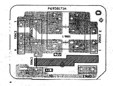
| ZD905 | 2339842M | ZD HZS6A2 | ∆L900 1 | 2272391 | LINE FILTER | |
| ZD 951 | 2339853M | ZD HZS7A3 | 6958171A | FILTER P. W. B | ||
| ZD952 | 2339902 | ZD HZS16-2 | ||||
| ZD953 | 2339847M | ZD HZS6C1 | ||||
| ZD954 | 2339869M | ZD HZS9C3 | ||||
| ZDR209 | 2331815A | ZD HZ7B2 | ||||
| ZK 119 | 2339837M | ZD HZS5C1 | ||||
| E063 | 2772982K | FERRITE SHEET | ||||
| E011 | 5780081A | ADAPTOR | ||||
| F013 | 2785601 | BATTERY AA1015 | ||||
| WI | 2076143 | CONNECTOR | 1 | |||
| 27507714 | BOD ANTENNA | |||||
| 2708105A | LED HOLDER | |||||
| 3746071A | ICE CORD HOLDER | · . | ||||
| 37637514 | SK BINDER | |||||
| 1150 49 4 A | SK DINDER | |||||
| 4159424A | SATUTAPPING SCREW WITH | |||||
| 4510740 | WASHER | |||||
| 4010742 | M2. SAIZ SCREW WITH | |||||
| 4510759 | 2 SMUT | |||||
| 4518753 | 2. 3MUI | |||||
| 4519501A | 3X10B-TIGHT TAPPING SCREW | |||||
| 4520883 | M3X12 TAPPING SCREW | |||||
| 4521392A | 5×25 SCREW W/WASHER | |||||
| 6030341A | BACK COVER | |||||
| 6010541A | FRAME ASSY(1471) | |||||
| 6010543A | FRAME ASSY(1473) | |||||
| 6010545A | FRAME ASSY (1470) | |||||
| 6250311A | HEAT SINK FOR IC 4501, | |||||
| IC681,Q781 | ||||||
| 6250321A | HEAT SINK FORQ903 | |||||
| 6450033A | RUBBER WASHER | |||||
| 7340112A | SPRING FOR KNOB | |||||
| 7340021A | EARTH SPRING | |||||
| 8781642A | 4X12TAPPING SCREW | |||||
| 8781646A | 4X16 TAPPING SCREW | |||||
| JK03202A | MAIN P. W. B | |||||
| L | L | I | ||||
CPT1470
CPT1470 CMT1473/1471

- 26
HITACHI
CPT1470 CMT1473 CMT1471 Fujian Hitachi Television Co., Ltd.
Printed in China


 Loading...