


PF0030 Series
MOS FET Power Amplifier
ADE-208-460 (Z) 1st Edition July 1996
Features
•High stability: Load VSWR = 20 : 1
•Low power control current: 400 A
•Thin package: 5 mmt
Ordering Information
Type No |
Operating Frequency |
Application |
PF0030 |
824 to 849 MHz |
AMPS |
|
|
|
PF0032 |
872 to 905 MHz |
E-TACS |
|
|
|
Pin Arrangement
∙ RF-B2 |
|
5 |
|
|
|
|
1: Pin |
|
|
4 |
2: VAPC |
|
3 |
3: VDD |
|
|
|
||
|
|
|
4: Pout |
5 |
2 |
|
5: GND |
1 |
|
|
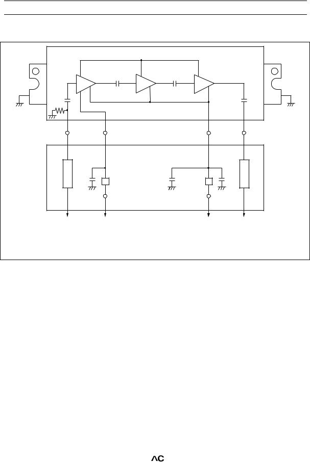
PF0030 Series
Internal Diagram and External Circuit
G |
|
|
|
|
|
G |
GND |
|
|
|
|
|
GND |
Pin1 |
|
Pin2 |
|
Pin3 |
|
Pin4 |
Pin |
|
VAPC |
|
VDD |
|
Pout |
Z1 |
C1 |
FB1 |
C3 |
FB2 |
C2 |
Z2 |
Pin |
|
VAPC |
|
VDD |
|
Pout |
C1 = C2 = 0.01 μF (Ceramic chip capacitor) |
|
|
|
|
||
C3 = 10 μF (Aluminum Electrolyte Capacitor) |
|
|
|
|
||
FB = Ferrite bead BL01RN1-A62-001 (Manufacture: MURATA) or equivalent |
|
|||||
Z1 = Z2 = 50 Ω (Microstrip line) |
|
|
|
|
||
Absolute Maximum Ratings (Ta = 25°C)
Item |
Symbol |
|
|
|
|
|
|
|
|
|
|
|
|
Rating |
Unit |
||||
Supply voltage |
VDD |
17 |
V |
||||||||||||||||
Supply current |
IDD |
3 |
A |
||||||||||||||||
APC voltage |
VAPC |
±8 |
V |
||||||||||||||||
Input power |
Pin |
20 |
mW |
||||||||||||||||
|
|
|
|
|
|
|
|
|
|
|
|
|
|
|
|
||||
Operating case temperature |
Tc (op) |
|
|
|
|
|
|
|
|
|
|
|
|
–30 to +110 |
°C |
||||
Storage temperature |
Tstg |
|
|
|
|
|
|
|
|
|
|
|
|
–40 to +110 |
°C |
||||
|
|
|
|
|
|
|
|
|
|
|
|
|
|
|
|
|
|
|
|
2
PF0030 Series
Electrical Characteristics (Ta = 25°C)
Item |
Symbol |
Min |
Typ |
Max |
Unit |
|
Test Condition |
|
Drain cutoff current |
IDS |
— |
— |
500 |
µA |
|
VDD = 17 V, VAPC = 0 V |
|
Total efficiency |
ηT |
35 |
40 |
— |
% |
Pin = 2 mW, |
|
|
|
|
|
|
|
|
|
|
|
2nd harmonic distortion |
2nd H.D. |
— |
–50 |
–30 |
dB |
V DD = 12.5 V, |
|
|
|
|
|
|
|
|
|
|
|
3rd harmonic distortion |
3rd H.D. |
— |
–50 |
–30 |
dB |
Pout = 6 W (at APC controlled) |
||
|
|
|
|
|
|
|
|
Ω |
Input VSWR |
VSWR (in) |
— |
1.5 |
3 |
— |
Zin = Zout = 50 |
||
|
|
|
|
|
|
|
|
|
Output VSWR |
VSWR (out) |
— |
1.5 |
— |
— |
|
|
|
|
|
|
|
|
|
|||
Stability |
— |
No parasitic oscillation |
— |
Pin = 2 mW, V |
DD = 12.5 V, |
|||
Pout = 6 W (at APC controlled), Zin = 50 Ω,
Output VSWR = 20:1 All phases, t = 20 sec
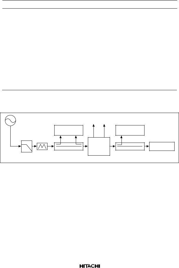
Test System Diagram
S.G |
|
VAPC |
VDD |
|
|
Power |
|
|
Spectrum |
|
Meter |
|
|
Analyzer |
L.P.F |
3dB |
|
|
|
ATT |
|
|
|
|
|
Test |
|
||
|
|
Power Meter |
||
|
|
Fixture |
||
|
|
|
||
|
Directional |
|
|
Directional |
|
Coupler |
|
|
Coupler |
3

PF0030 Series
Test Fixture Pattern
Unit: mm
|
26.5 |
2.88 |
2.88 |
28 |
|
|
|
3.5 |
4.5 3 |
16 |
6 |
4 |
|
|
|
|
|
4 |
|
|
|
|
|
|
1.5 |
|
|
|
|
|
VAPC |
VDD |
|
80 |
|
|
|
|
|
|
|
2.88 |
4 |
|
|
|
3.5 |
2.88 |
|
|
|
|
|
4 |
16.5 |
15 |
4 |
|
|
|
|
|
|
|
|
|
100 |
|
|
Grass Epoxy Double sided PCB |
|
|
|
|
||
(t = 1.6 mm, εr = 4.8) |
|
|
|
|
|
|
Mechanical Characteristics
Item |
Conditions |
Spec |
Torque for screw up the heatsink flange |
M3 Screw Bolts |
4 to 6 kg•cm |
Warp size of the heatsink flange: S |
|
S = 0 |
|
|
+0.3/–0 mm |
|
|
S |
4

PF0030 Series
Note for Use
•Unevenness and distortion at the surface of the heatsink attached module should be less than 0.05 mm.
•It should not be existed any dust between module and heatsink.
•MODULE should be separated from PCB less than 1.5 mm.
•Soldering temperature and soldering time should be less than 230°C, 10 sec. (Soldering position spaced from the root point of the lead frame: 2 mm)
•Recommendation of thermal joint compounds is TYPE G746. (Manufacturer: Shin-Etsu Chemical, Co., Ltd.)
•To protect devices from electro-static damage, soldering iron, measuring-equipment and human body etc. should be grounded.
•Torque for screw up the heatsink flange should be 4 to 6 kg · cm with M3 screw bolts.
•Don’t solder the flange directly.
•It should make the lead frame as straight as possible.
•The module should be screwed up before lead soldering.
•It should not be given mechanical and thermal stress to lead and flange of the module.
•When the external parts (Isolator, Duplexer, etc.) of the module are changed, the electrical characteristics should be evaluated enough.
•Don’t washing the module except lead pins.
•To get good stability, ground impedance between the module GND flange and PCB GND pattern should be designed as low as possible.
5
PF0030 Series
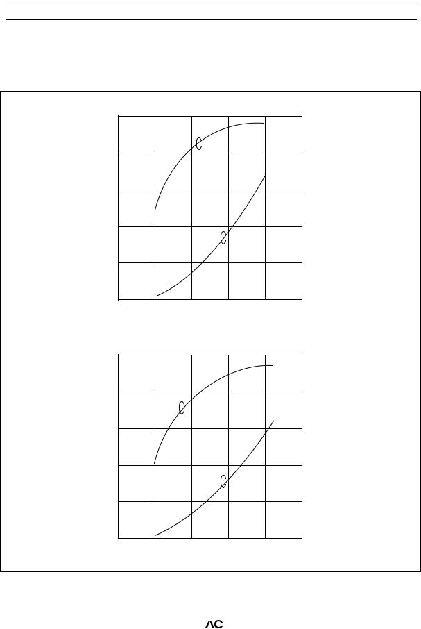
Characteristics Curve
PF0030
|
20 |
|
|
16 |
|
(W) |
|
|
Pout |
12 |
|
|
||
Power |
8 |
|
Output |
||
|
||
|
4 |
|
|
0 |
0
|
20 |
|
|
16 |
|
(W) |
|
|
Pout |
12 |
|
|
||
Power |
8 |
|
Output |
||
|
||
|
4 |
|
|
0 |
0
Pout, ηT vs. VDD (1)
|
ηT |
|
|
|
|
|
|
|
|
|
|
50 |
|
|||||||||||
|
|
|
|
|
|
|
|
|
|
|
||||||||||||||
|
|
|
|
|
|
|
|
|
|
|
|
|
||||||||||||
|
|
|
|
|
|
|
|
|
|
|
|
|
|
|
|
|
|
|
|
|
|
|
40 |
|
|
|
|
|
|
|
|
|
|
|
|
|
|
|
|
|
|
|
|
|
|
|
|
30 |
(%) |
|
|
|
|
|
|
|
|
|
|
|
|
|
|
|
|
|
|
|
|
|
|
|
T |
|
|
|
|
|
|
|
|
|
|
|
|
|
|
|
|
|
|
|
|
|
|
|
|
|
η |
|
|
|
|
|
|
|
|
|
|
|
|
|
|
|
|
|
|
|
|
|
|
|
20 |
Efficiency |
|
|
|
|
|
|
|
|
|
|
|
|
|
|
|
|
|
|
|
|
|
|
|
|
|
|
|
|
|
|
|
|
Pout |
|
|
|
|
|
|
|
|
|
|
|
|
|||||
|
|
|
|
|
|
|
|
|
|
|
|
|
|
|
|
|
|
|
|
|
|
|
10 |
|
|
|
|
|
|
|
|
|
|
|
|
|
|
|
|
|
|
|
|
|
f = 824 MHz |
|
|
|
|
|
|
|
|
|
|
|
|
|
|
|
|
|
|
|
|
|
|
|
|
Pin = 2 mW |
|
|
|
|
|
|
|
|
|
|
|
|
|
|
|
|
|
|
|
|
|
|
|
|
VAPC = 4 V |
|
|
|
|
|
|
|
|
|
|
|
|
|
|
|
|
|
|
|
|
|
|
|
|
|
|
|
0 |
|
|
|
|
|
|
|
|
|
|
|
|
|
|
|
|
|
|
|
|
|
|
|
|
||
4 |
8 |
|
|
|
|
|
|
|
|
12 |
|
|
16 |
20 |
|
|||||||||
|
Supply Voltage VDD (V) |
|
|
|
|
|||||||||||||||||||
|
Pout, ηT vs. VDD (2) |
|
|
|
|
|
||||||||||||||||||
|
|
|
|
|
|
|
|
|
|
|
|
|
|
|
|
|
|
|
|
|
|
|
50 |
|
|
|
|
|
|
|
|
|
|
|
|
|
|
|
|
|
|
|
|
|
|
|
|
||
|
ηT |
|
|
|
|
|
|
|
|
|
|
40 |
|
|||||||||||
|
|
|
|
|
|
|
|
|
|
|
|
(%) |
||||||||||||
|
|
|
|
|
|
|
|
|
|
|
|
|
|
|
|
|
|
|
|
|
|
|
30 |
|
|
|
|
|
|
|
|
|
|
|
|
|
|
|
|
|
|
|
|
|
|
|
|
T |
|
|
|
|
|
|
|
|
|
|
|
|
|
|
|
|
|
|
|
|
|
|
|
|
|
η |
|
|
|
|
|
|
|
|
|
|
|
|
|
|
|
|
|
|
|
|
|
|
|
20 |
Efficiency |
|
|
|
|
|
|
|
|
|
|
|
|
|
|
|
|
|
|
|
|
|
|
|
|
|
|
|
|
|
|
|
|
Pout |
|
|
|
|
|
|
|
|
|
|
|
|
|||||
|
|
|
|
|
|
|
|
|
|
|
|
|
|
|
|
|
|
|
|
|
|
|
10 |
|
|
|
|
|
|
|
|
|
|
|
|
|
|
|
|
|
|
|
|
|
f = 849 MHz |
|
|
|
|
|
|
|
|
|
|
|
|
|
|
|
|
|
|
|
|
|
|
|
|
Pin = 2 mW |
|
|
|
|
|
|
|
|
|
|
|
|
|
|
|
|
|
|
|
|
|
|
|
|
VAPC = 4 V |
|
|
|
|
|
|
|
|
|
|
|
|
|
|
|
|
|
|
|
|
|
|
|
|
|
|
|
0 |
|
|
|
|
|
|
|
|
|
|
|
|
|
|
|
|
|
|
|
|
|
|
|
|
||
4 |
8 |
|
|
|
|
|
|
|
|
12 |
|
|
16 |
20 |
|
|||||||||
|
Supply Voltage |
VDD (V) |
|
|
|
|
||||||||||||||||||
|
|
|
|
|
|
|
|
|
|
|
|
|
|
|
|
|
|
|
|
|
|
|
|
|
6
 Loading...