


HAMAMATSU F2224-31, F2224-29P, F2224-29M, F2224-24S, F2224-24P Datasheet
...CIRCULAR MCP AND ASSEMBLY SERIES
A microchannel plate (MCP) is a secondary-electron multiplier which detects and amplifies electrons in two-dimen- sions. The MCP is sensitive not only to electrons but to ions, vacuum ultraviolet light, X-rays and γ-rays, making it useful in a wide range of detection applications.
Hamamatsu has available seven types of circular MCPs, ranging in outer diameter from 18mm to 114mm. MCP assemblies with electrode leads are also available to facilitate use of the MCPs. These MCP assemblies offer three types of read-out devices; a phosphor screen (optical image conversion), a multi-anode (electrical output signals responding to the position of the incident signals), and a single-anode (an electrical output signal within the effective area), providing a variety of readout functions to handle a range of applications. From one to three MCPs can be selected as required to provide the necessary electron gain.
These MCPs and MCP assemblies are finding wide application in fields including image intensifiers, fast time response photomultiplier tubes, and analytical instruments.
FEATURES
•Sensitive to electrons, ions, VUV lights, X-rays and γ-rays
•Two-dimensional image intensification
•Fast time response
•Immunity to magnetic fields
•Small size and lightweight
APPLICATIONS
•Analytical Instruments
•Electron Beam Measuring System (EBMS)
•FIM, AP-FIM
•ESCA
•Mass Spectrometer (MS)
•TOF-MS
•LEED, MEED, etc.
•Electron Tube
•Image Intensifier
•Fast Time Response PMT
•Streak Camera
•Cosmic Measurement
•Detection of Plasma Ions, Soft X-rays and VUV lights
•High Energy Physics
•Detection of Ions, Electrons, Positrons, High Energy Particles and X-rays
Subject to local technical requirements and regulations, availability of products included in this promotional material may vary. Please consult with our sales office.
Information furnished by HAMAMATSU is believed to be reliable. However, no responsibility is assumed for possible inaccuracies or omissions. Specifications are subject to change without notice. No patent rights are granted to any of the circuits described herein. ©1999 Hamamatsu Photoni cs K.K
CIRCULAR MCP SERIES
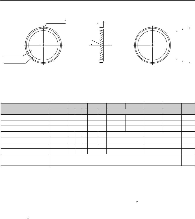
MCP DIMENSIONAL OUTLINES (Unit: mm)
D
INDICATOR
θ
EFFECTIVE
AREA
ELECTRODE
INPUT SIDE
|
|
|
|
|
|
|
|
|
|
|
|
|
|
|
C |
|
|
B |
|
A |
|
|
|
|
|
|
|
|
|
|||
|
|
|
|
|
|
|
||||
|
|
|
|
|
|
|
|
|
|
|
|
|
|
|
|
|
|
|
|
|
|
|
|
|
|
|
|
|
|
|
|
|
|
|
|
|
|
|
|
|
|
|
|
OUTPUT SIDE
TMCPA0025EB
|
Type No. |
F1551 |
F1094 |
F1552 |
F1208 |
F1217 |
F1942 |
F2395 |
Unit |
|||
Parameter |
|
-01 |
-07 -09 -01 |
-09 |
-01 |
|
-01 |
-04 |
|
|||
|
|
|
|
|||||||||
Outer Diameter |
A |
17.9 |
|
24.8 |
|
32.8 |
38.5 |
49.9 |
86.7 |
114 |
mm |
|
Electrode Diameter |
B |
17 |
|
23.9 |
|
31.8 |
36.5 |
49 |
84.7 |
112 |
mm |
|
Effective Diameter |
C |
14.5 |
|
20 |
|
27 |
32 |
42 |
77 |
105 |
mm |
|
Thickness |
D |
0.48 |
0.24 0.41 0.48 |
0.41 |
0.48 |
|
0.48 |
1.00 |
|
mm |
||
Channel Diameter |
|
12 |
6 |
10 |
12 |
10 |
12 |
|
12 |
25 |
|
m |
Channel Pitch |
|
15 |
7.5 |
12 |
15 |
12 |
15 |
|
15 |
31 |
|
m |
Bias Angle |
θ |
8 |
13 |
5,15 5,8,15 |
8,12 |
|
8 |
8 |
|
degrees |
||
Open Area Ratio |
60 |
% |
Electrode Material |
Inconel |
— |
ELECTRICAL CHARACTERISTICS
(Supply Voltage: 1000V, Vacuum: 1.3 × 10⁻⁴ Pa (1 × 10⁻⁶ Torr), Ambient Temperature: +25°C)
Gain |
|
|
More than 104 |
|
— |
|||
Plate Resistance |
100 to 700 |
50 to 500 |
30 to 300 |
20 to 200 |
10 to 200 |
10 to 100 |
5 to 50 |
MΩ |
|
|
|
|
|
|
|
|
|
Dark Current |
|
|
Less than 5 × 10-13 |
|
A/cm3 |
|||
Max. Linear Output Signal |
|
|
Up to 7% of the strip current |
|
— |
|||
|
|
|
|
|
|
|
|
|
MAXIMUM RATINGS
Supply Voltage |
1000 (Channel Diameter: 6μm, 10μm, 12μm): 1200 (Channel Diameter: 25μm) |
V |
|
|
|
|
|
Ambient Temperature |
-50 to +70 |
-50 to +30 |
°C |
|
|
|
|
Baking Temperature |
400 |
|
°C |
|
|
|
|
 This indicator shows the MCP input side and the direction of channel bias.
 The strip current is the current which flows along the channel wall when a voltage is applied between the MCP input and output and is given by applied voltage/plate resistance.
 At a vacuum of 1.3 × 10⁻⁴ Pa (1 × 10⁻⁶ Torr) or less.
Consult us for more details on MCP dimensions and tolerances.

OPERATING PRINCIPLE
As shown in the figure, when a voltage VD is applied across the input-side and output-side electrodes of the MCP, a potential gradient is built up along the channel direction. If an incident electron strikes an inner wall on the input side, a number of secondary electrons are emitted. These secondary electrons are accelerated by the potential gradient and travel along a parabolic path determined by the initial velocity. They then collide with the opposing wall surface, causing secondary electrons to be emitted again. In this manner, the electrons collide repeatedly within the channel as they pass towards the output side. The result is a large multiplication of the incident electron.
GAIN AND LIFE CHARACTERISTICS
• Gain vs. Supply Voltage
TMCPB0031EB
105
104
GAIN
103
102
600 |
800 |
1000 |
MCP CONFIGURATION
|
PRIMARY |
CHANNEL WALL |
|
|
|
ELECTRON |
|
|
|
|
|
|
|
OUTPUT |
|
|
|
|
ELECTRONS |
|
|
STRIP CURRENT |
|
|
|
|
VD |
|
TMCPC0002EC |
|
|
|
|
|
|
• Life |
|
|
|
|
TMCPB0030EC |
|
|
|
|
1.0 |
|
|
|
OUTPUT |
|
|
|
|
RELATIVE |
0.5 |
|
|
|
|
|
|
|
|
|
SUPPLY VOLTAGE: 1000V |
|
|
|
|
OUTPUT CURRENT DENSITY: 50nA/ |
15mm |
|
|
|
0 |
|
|
|
|
10-4 |
10-3 |
10-2 |
10-1 |
ACCUMULATED CHARGE OF OUTPUT SIGNAL (C / cm2)
SUPPLY VOLTAGE (V)
 Loading...