


GS881Z18T-66I
GSI GS881Z18T-66I, GS881Z18T-66, GS881Z18T-11I, GS881Z18T-11, GS881Z18T-100I Datasheet
...
Preliminary
GS881Z18/36T-11/100/80/66
100-Pin TQFP
8Mb Pipelined and Flow Through
Commercial Temp
Industrial Temp
Synchronous NBT SRAMs
Features
• 512K x 18 and 256K x 36 configurations
• User-configurable Pipelined and Flow Through mode
• NBT (No Bus Turn Around) functionality allows zero wait
• Read-Write-Read bus utilization
• Fully pin-compatible with both pipelined and flow through
NtRAM™, NoBL™ and ZBT™ SRAMs
• IEEE 1149.1 JTAG-compatible Boundary Scan
• On-chip write parity checking; even or odd selectable
• Pin-compatible with 2M, 4M and 16M devices
• 3.3 V +10%/–5% core power supply
• 2.5 V or 3.3 V I/O supply
• LBO
pin for Linear or Interleave Burst mode
• Byte write operation (9-bit Bytes)
• 3 chip enable signals for easy depth expansion
• Clock Control, registered, address, data, and control
• ZZ Pin for automatic power-down
• JEDEC-standard 100-lead TQFP package
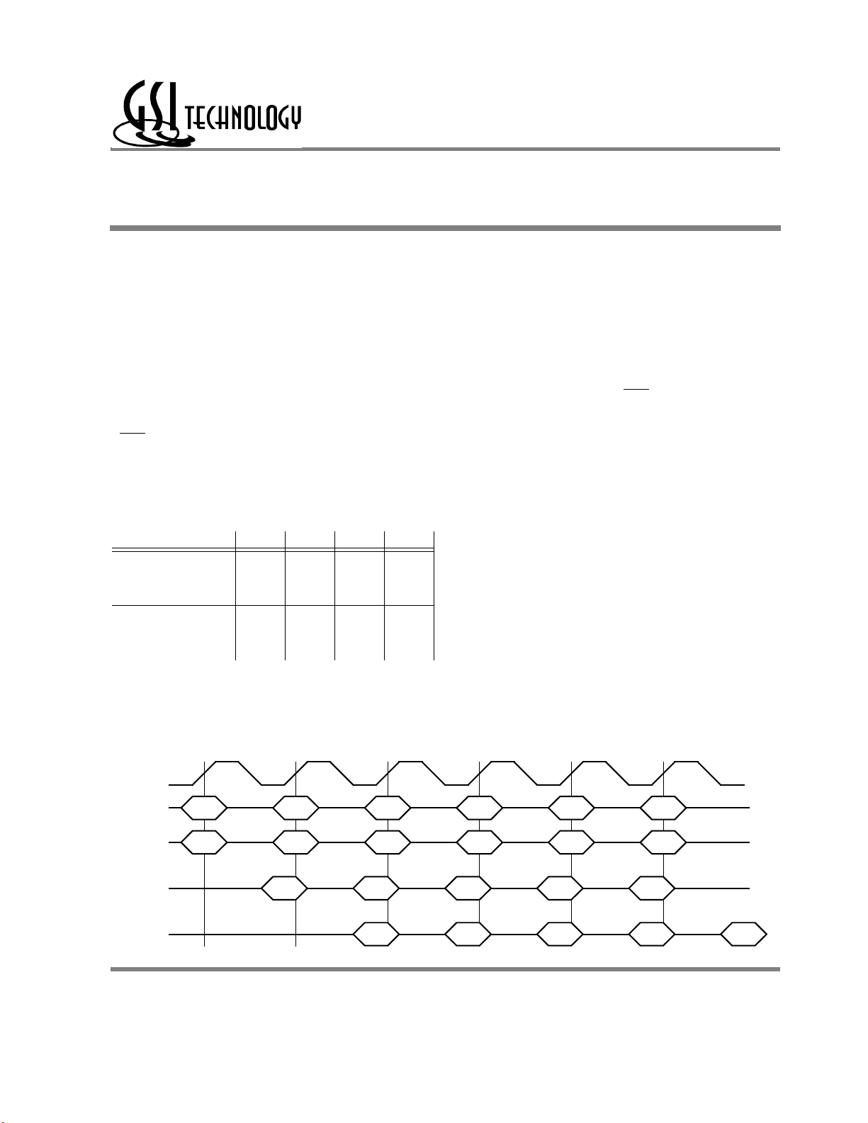
-11 -100 -80 -66
t
Pipeline
3-1-1-1
Flow Through
2-1-1-1
Cycle
t
I
t
t
Cycle
I
KQ
DD
KQ
DD
10 ns
4.5 ns
210 mA
11 ns
15 ns
150 mA
10 ns
4.5 ns
210 mA
12 ns
15 ns
150 mA
12.5 ns
4.8 ns
190 mA
14 ns
15 ns
130 mA
15 ns
5 ns
170 mA
18 ns
20 ns
130 mA
100 MHz–66 MHz
3.3 V V
2.5 V and 3.3 V V
DD
DDQ
Functional Description
The GS881Z18/36T is an 8Mbit Synchronous Static SRAM.
GSI's NBT SRAMs, like ZBT, NtRAM, NoBL or other
pipelined read/double late write or flow through read/single
late write SRAMs, allow utilization of all available bus
bandwidth by eliminating the need to insert deselect cycles
when the device is switched from read to write cycles.
Because it is a synchronous device, address, data inputs, and
read/ write control inputs are captured on the rising edge of the
input clock. Burst order control (LBO) must be tied to a power
rail for proper operation. Asynchronous inputs include the
Sleep mode enable (ZZ) and Output Enable. Output Enable can
be used to override the synchronous control of the output
drivers and turn the RAM's output drivers off at any time.
Write cycles are internally self-timed and initiated by the rising
edge of the clock input. This feature eliminates complex offchip write pulse generation required by asynchronous SRAMs
and simplifies input signal timing.
The GS881Z18/36T may be configured by the user to operate
in Pipeline or Flow Through mode. Operating as a pipelined
synchronous device, in addition to the rising-edge-triggered
registers that capture input signals, the device incorporates a
rising-edge-triggered output register. For read cycles, pipelined
SRAM output data is temporarily stored by the edge-triggered
output register during the access cycle and then released to the
output drivers at the next rising edge of clock.
The GS881Z18/36T is implemented with GSI's high
performance CMOS technology and is available in a JEDECStandard 100-pin TQFP package.
Flow Through and Pipelined NBT SRAM Back-to-Back Read/Write Cycles
Clock
Address
Read/Write
Flow Through
Data I/O
Pipelined
Data I/O
Rev: 1.10 8/2000 1/34 © 1998, Giga Semiconductor, Inc.
Specifications cited are subject to change without notice. For latest documentation see http://www.gsitechnology.com.
NoBL is a trademark of Cypress Semiconductor Corp.. NtRAM is a trademark of Samsung Electronics Co.. ZBT is a trademark of Integrated Device Technology, Inc.
A B C D E F
R W R W R W
Q
A
D
B
Q
A
Q
C
D
B
D
D
Q
C
Q
E
D
D
Q
E

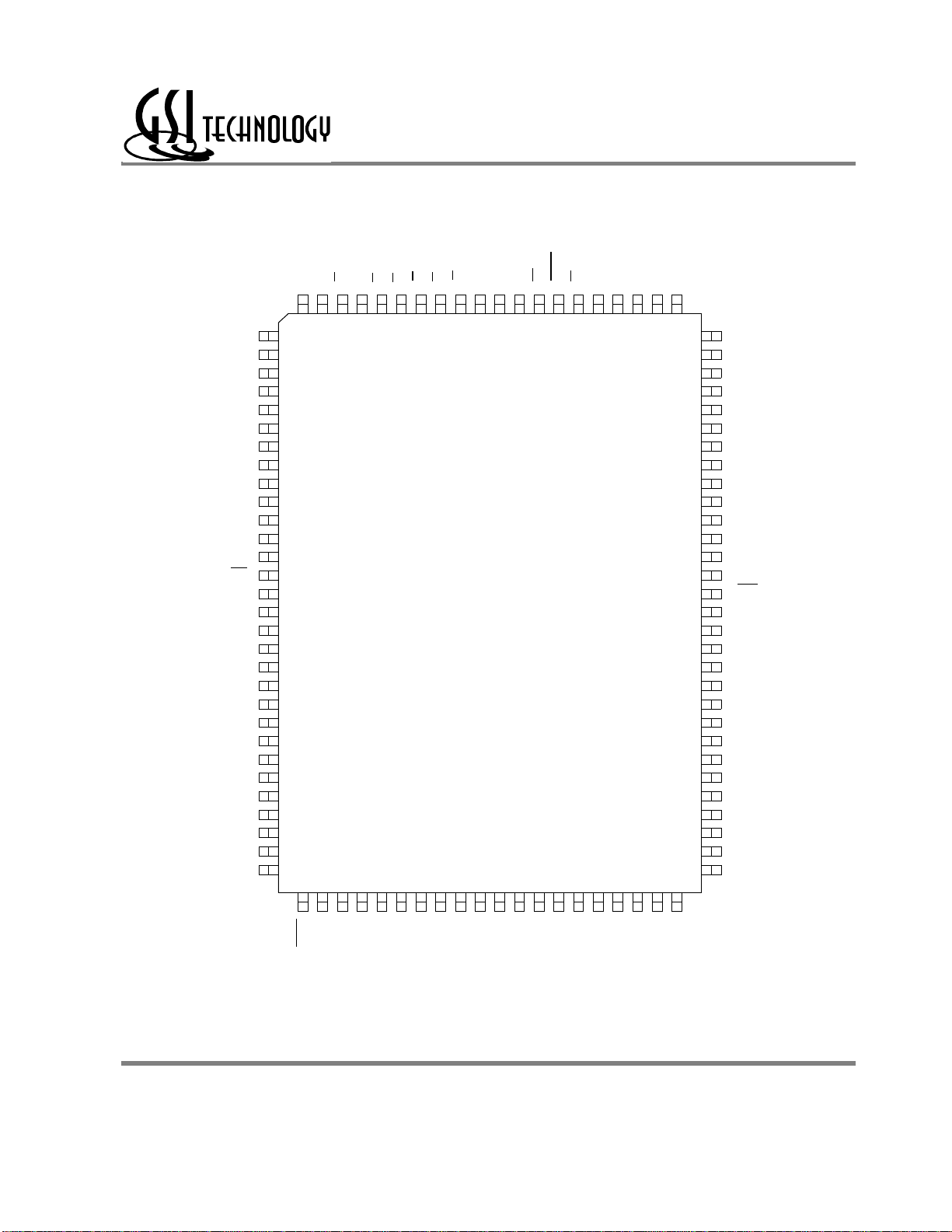
GS881Z18T Pinout
Preliminary.
GS881Z18/36T-11/100/80/66
DD
SS
A6
E1
A7
E2
NC
NC
E3
BB
V
BA
V
CKE
W
G
CK
ADV
A8
A17
NC
A9
NC
NC
NC
V
DDQ
V
NC
NC
DQB1
DQB2
V
V
DDQ
DQB3
DQB4
V
DP
V
DQB5
DQB6
V
DDQ
V
DQB7
DQB8
DQB9
NC
V
V
DDQ
NC
NC
NC
SS
SS
FT
DD
SS
SS
SS
100 99 98 97 96 95 94 93 92 91 90 89 88 87 86 85 84 83 82 81
1
2
3
4
5
6
7
8
9
10
11
12
13
14
15
16
17
18
19
20
21
22
23
24
25
26
27
28
29
30
31 32 33 34 35 36 37 38 39 40 41 42 43 44 45 46 47 48 49 50
512K x 18
Top View
80
79
78
77
76
75
74
73
72
71
70
69
68
67
66
65
64
63
62
61
60
59
58
57
56
55
54
53
52
51
A18
NC
NC
V
DDQ
V
SS
NC
DQA9
DQA8
DQA7
V
SS
V
DDQ
DQA6
DQA5
V
SS
QE
V
DD
ZZ
DQA4
DQA3
V
DDQ
V
SS
DQA2
DQA1
NC
NC
V
SS
V
DDQ
NC
NC
NC
SS
A5
A4
A3
A2
A1
LBO
A0
TMS
DD
V
V
TDI
TDO
A11
A10
A12
A13
A14
A16
TCK
A15
Rev: 1.10 8/2000 2/34 © 1998, Giga Semiconductor, Inc.
Specifications cited are subject to change without notice. For latest documentation see http://www.gsitechnology.com
GS881Z36T Pinout
Preliminary.
GS881Z18/36T-11/100/80/66
DD
SS
A6
E1
A7
E2
BC
BD
E3
BB
V
BA
V
CKE
W
G
CK
ADV
A8
A17
NC
A9
DQC9
DQC8
DQC7
V
DDQ
V
DQC6
DQC5
DQC4
DQC3
V
V
DDQ
DQC2
DQC1
V
DP
V
DQD1
DQD2
V
DDQ
V
DQD3
DQD4
DQD5
DQD6
V
V
DDQ
DQD7
DQD8
DQD9
SS
SS
FT
DD
SS
SS
SS
100 99 98 97 96 95 94 93 92 91 90 89 88 87 86 85 84 83 82 81
1
2
3
4
5
6
7
8
9
10
11
12
13
14
15
16
17
18
19
20
21
22
23
24
25
26
27
28
29
30
31 32 33 34 35 36 37 38 39 40 41 42 43 44 45 46 47 48 49 50
256K x 36
Top View
80
79
78
77
76
75
74
73
72
71
70
69
68
67
66
65
64
63
62
61
60
59
58
57
56
55
54
53
52
51
DQB9
DQB8
DQB7
V
DDQ
V
SS
DQB6
DQB5
DQB4
DQB3
V
SS
V
DDQ
DQB2
DQB1
V
SS
QE
V
DD
ZZ
DQA1
DQA2
V
DDQ
V
SS
DQA3
DQA4
DQA5
DQA6
V
SS
V
DDQ
DQA7
DQA8
DQA9
SS
A5
A4
A3
A2
A1
LBO
A0
TMS
DD
V
V
TDI
TDO
A11
A10
A12
A13
A14
A16
TCK
A15
Rev: 1.10 8/2000 3/34 © 1998, Giga Semiconductor, Inc.
Specifications cited are subject to change without notice. For latest documentation see http://www.gsitechnology.com
GS881Z18/36T-11/100/80/66
100-Pin TQFP Pin Descriptions
Pin Location Symbol Type Description
37, 36 A0, A1 In Burst Address Inputs—Preload the burst counter
35, 34, 33, 32, 100, 99, 83, 82,
81, 50, 49, 48, 47, 46, 45, 44
80 A18 In Address Input (x18 Version Only)
89 CK In Clock Input Signal
93 BA In Byte Write signal for data inputs DQA1–DQA9; active low
94 BB In Byte Write signal for data inputs DQB1–DQB9; active low
95 BC In Byte Write signal for data inputs DQC1–DQC9; active low (x36 Version Only)
96 BD In Byte Write signal for data inputs DQD1–DQD9; active low (x36 Version Only)
88 W In Write Enable; active low
98 E1 In Chip Enable; active low
97 E2 In Chip Enable; active high; for self decoded depth expansion
92 E3 In Chip Enable; active low; for self decoded depth expansion
86 G In Output Enable; active low
85 ADV In Advance/Load—Burst address counter control pin
87 CKE In Clock Input Buffer Enable; active low
58, 59, 62,63, 68, 69, 72, 73, 74 DQA1–DQA9 I/O Byte A Data Input and Output pins (x18 Version Only)
8, 9, 12, 13, 18, 19, 22, 23, 24 DQB1–DQB9 I/O Byte B Data Input and Output pins (x18 Version Only)
51, 52, 53, 56, 57, 75, 78, 79,
1, 2, 3, 6, 7, 25, 28, 29, 30
51, 52, 53, 56, 57, 58, 59, 62,63 DQA1–DQA9 I/O Byte A Data Input and Output pins (x36 Versions Only)
68, 69, 72, 73, 74, 75, 78, 79, 80 DQB1–DQB9 I/O Byte B Data Input and Output pins (x36 Versions Only)
1, 2, 3, 6, 7, 8, 9, 12, 13 DQC1–DQC9 I/O Byte C Data Input and Output pins (x36 Versions Only)
18, 19, 22, 23, 24, 25, 28, 29, 30 DQD1–DQD9 I/O Byte D Data Input and Output pins (x36 Versions Only)
64 ZZ In Power down control; active high
14 FT In Pipeline/Flow Through Mode Control; active low
31 LBO In Linear Burst Order; active low
A2–A17 In Address Inputs
NC — No Connect (x18 Version Only)
Preliminary.
Rev: 1.10 8/2000 4/34 © 1998, Giga Semiconductor, Inc.
Specifications cited are subject to change without notice. For latest documentation see http://www.gsitechnology.com
Pin Location Symbol Type Description
38 TMS — Scan Test Mode Select
39 TDI — Scan Test Data In
42 TDO — Scan Test Data Out
43 TCK — Scan Test Clock
15, 41, 65, 91
5,10, 17, 21, 26, 40, 55, 60, 67,
71, 76, 90
4, 11, 20, 27, 54, 61, 70, 77
16 DP In Parity Input—1 = Even, 0 = Odd
66 QE Out Parity Error Out—Open Drain Output
42, 43,, 84 NC — No Connect
V
DD
V
SS
V
DDQ
In 3.3 V power supply
In Ground
In 3.3 V output power supply for noise reduction
Preliminary.
GS881Z18/36T-11/100/80/66
Rev: 1.10 8/2000 5/34 © 1998, Giga Semiconductor, Inc.
Specifications cited are subject to change without notice. For latest documentation see http://www.gsitechnology.com
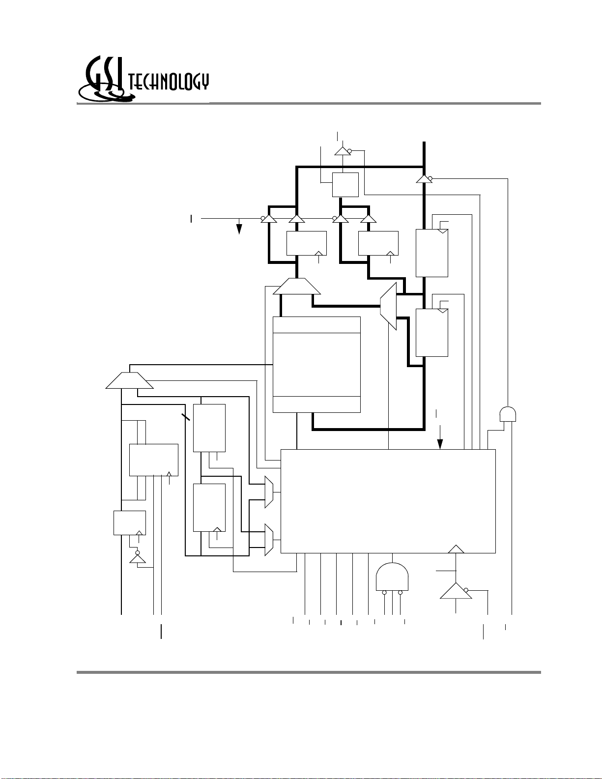
GS881Z18/36 ByteSafe NBT SRAM Functional Block Diagram
A
Preliminary.
GS881Z18/36T-11/100/80/66
QE
DP
DQa–DQn
Parity
Check
FT
D Q
K
Sense Amps
Array
Memory
Write Drivers
D Q
K
Write Data
Write Data
K
Register 1
K
Register 2
FT
SA1’
SA0’
Burst
Counter
SA1
SA0
18
Register 2
Write Address
K
K
Register 1
D Q
K
LBO
0–An
ADV
Write Address
K
Match
Read, Write and
W
BA
Control Logic
Data Coherency
K
E3
E2
BB
BC
E1
BD
CK
G
CKE
Rev: 1.10 8/2000 6/34 © 1998, Giga Semiconductor, Inc.
Specifications cited are subject to change without notice. For latest documentation see http://www.gsitechnology.com
Preliminary.
GS881Z18/36T-11/100/80/66
Functional Details
Clocking
Deassertion of the Clock Enable (CKE) input blocks the Clock input from reaching the RAM's internal circuits. It may be used to
suspend RAM operations. Failure to observe Clock Enable set-up or hold requirements will result in erratic operation.
Pipeline Mode Read and Write Operations
All inputs (with the exception of Output Enable, Linear Burst Order and Sleep) are synchronized to rising clock edges. Single cycle
read and write operations must be initiated with the Advance/Load pin (ADV) held low, in order to load the new address. Device
activation is accomplished by asserting all three of the Chip Enable inputs (E1, E2, and E3). Deassertion of any one of the Enable
inputs will deactivate the device.
Function W BA BB BC BD
Read H X X X X
Write Byte “a” L L H H H
Write Byte “b” L H L H H
Write Byte “c” L H H L H
Write Byte “d” L H H H L
Write all Bytes L L L L L
Write Abort/NOP L H H H H
Read operation is initiated when the following conditions are satisfied at the rising edge of clock: CKE is asserted Low, all three
chip enables (E1, E2, and E3) are active, the write enable input signals W is deasserted high, and ADV is asserted low. The address
presented to the address inputs is latched in to address register and presented to the memory core and control logic. The control
logic determines that a read access is in progress and allows the requested data to propagate to the input of the output register. At
the next rising edge of clock the read data is allowed to propagate through the output register and onto the Output pins.
Write operation occurs when the RAM is selected, CKE is active and the Write input is sampled low at the rising edge of clock.
The Byte Write Enable inputs (BA, BB, BC, and BD) determine which bytes will be written. All or none may be activated. A Write
Cycle with no Byte Write inputs active is a no-op cycle. The pipelined NBT SRAM provides double late write functionality,
matching the write command versus data pipeline length (2 cycles) to the read command versus data pipeline length (2 cycles). At
the first rising edge of clock, Enable, Write, Byte Write(s), and Address are registered. The Data In associated with that address is
required at the third rising edge of clock.
Flow Through Mode Read and Write Operations
Operation of the RAM in Flow Through mode is very similar to operations in Pipeline mode. Activation of a Read Cycle and the
use of the Burst Address Counter is identical. In Flow Through mode the device may begin driving out new data immediately after
new address are clocked into the RAM, rather than holding new data until the following (second) clock edge. Therefore, in Flow
Through mode the read pipeline is one cycle shorter than in Pipeline mode.
Write operations are initiated in the same way as well, but differ in that the write pipeline is one cycle shorter, preserving the ability
to turn the bus from reads to writes without inserting any dead cycles. While the pipelined NBT RAMs implement a double late
write protocol, in Flow Through mode a single late write protocol mode is observed. Therefore, in Flow Through mode, address
and control are registered on the first rising edge of clock and data in is required at the data input pins at the second rising edge of
clock.
Rev: 1.10 8/2000 7/34 © 1998, Giga Semiconductor, Inc.
Specifications cited are subject to change without notice. For latest documentation see http://www.gsitechnology.com
Preliminary.
GS881Z18/36T-11/100/80/66
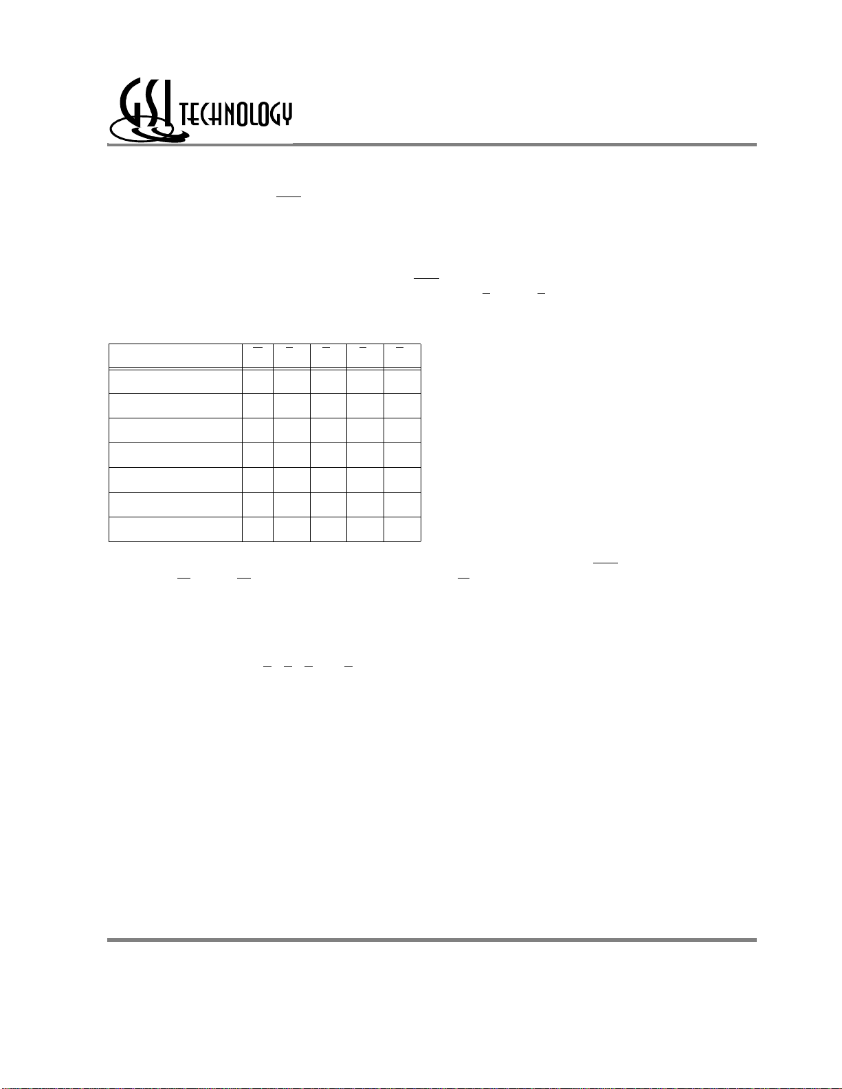
Synchronous Truth Table
Operation Type Address E1 E2 E3 ZZ ADV W Bx G CKE CK DQ Notes
Deselect Cycle, Power Down D None H X X L L X X X L L-H High-Z
Deselect Cycle, Power Down D None X X H L L X X X L L-H High-Z
Deselect Cycle, Power Down D None X L X L L X X X L L-H High-Z
Deselect Cycle, Continue D None X X X L H X X X L L-H High-Z 1
Read Cycle, Begin Burst R External L H L L L H X L L L-H Q
Read Cycle, Continue Burst B Next X X X L H X X L L L-H Q 1,10
NOP/Read, Begin Burst R External L H L L L H X H L L-H High-Z 2
Dummy Read, Continue Burst B Next X X X L H X X H L L-H High-Z 1,2,10
Write Cycle, Begin Burst W External L H L L L L L X L L-H D 3
Write Cycle, Continue Burst B Next X X X L H X L X L L-H D 1,3,10
NOP/Write Abort, Begin Burst W None L H L L L L H X L L-H High-Z 2,3
Write Abort, Continue Burst B Next X X X L H X H X L L-H High-Z 1,2,3,10
Clock Edge Ignore, Stall Current X X X L X X X X H L-H - 4
Sleep Mode None X X X H X X X X X X High-Z
Notes:
1. Continue Burst cycles, whether read or write, use the same control inputs; a Deselect continue cycle can only be entered into if a Deselect
cycle is executed first
2. Dummy read and write abort can be considered NOPs because the SRAM performs no operation. A Write abort occurs when the W pin is
sampled low but no Byte Write pins are active, so no Write operation is performed.
3. G can be wired low to minimize the number of control signals provided to the SRAM. Output drivers will automatically turn off during Write
cycles.
4. If CKE High occurs during a pipelined read cycle, the DQ bus will remain active (Low Z). If CKE High occurs during a write cycle, the bus
will remain in High Z.
5. X = Don’t Care; H = Logic High; L = Logic Low; Bx = High = All Byte Write signals are high; Bx = Low = One or more Byte/Write signals
are Low
6. All inputs, except G and ZZ must meet setup and hold times of rising clock edge.
7. Wait states can be inserted by setting CKE high.
8. This device contains circuitry that ensures all outputs are in High Z during power-up.
9. A 2-bit burst counter is incorporated.
10. The address counter is incriminated for all Burst continue cycles.
Rev: 1.10 8/2000 8/34 © 1998, Giga Semiconductor, Inc.
Specifications cited are subject to change without notice. For latest documentation see http://www.gsitechnology.com
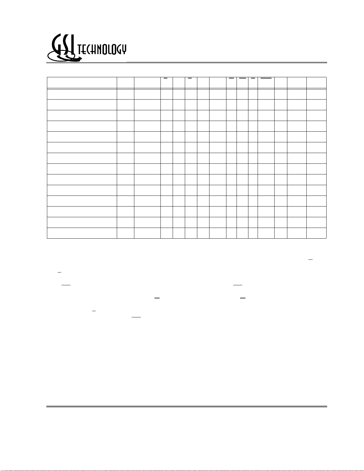
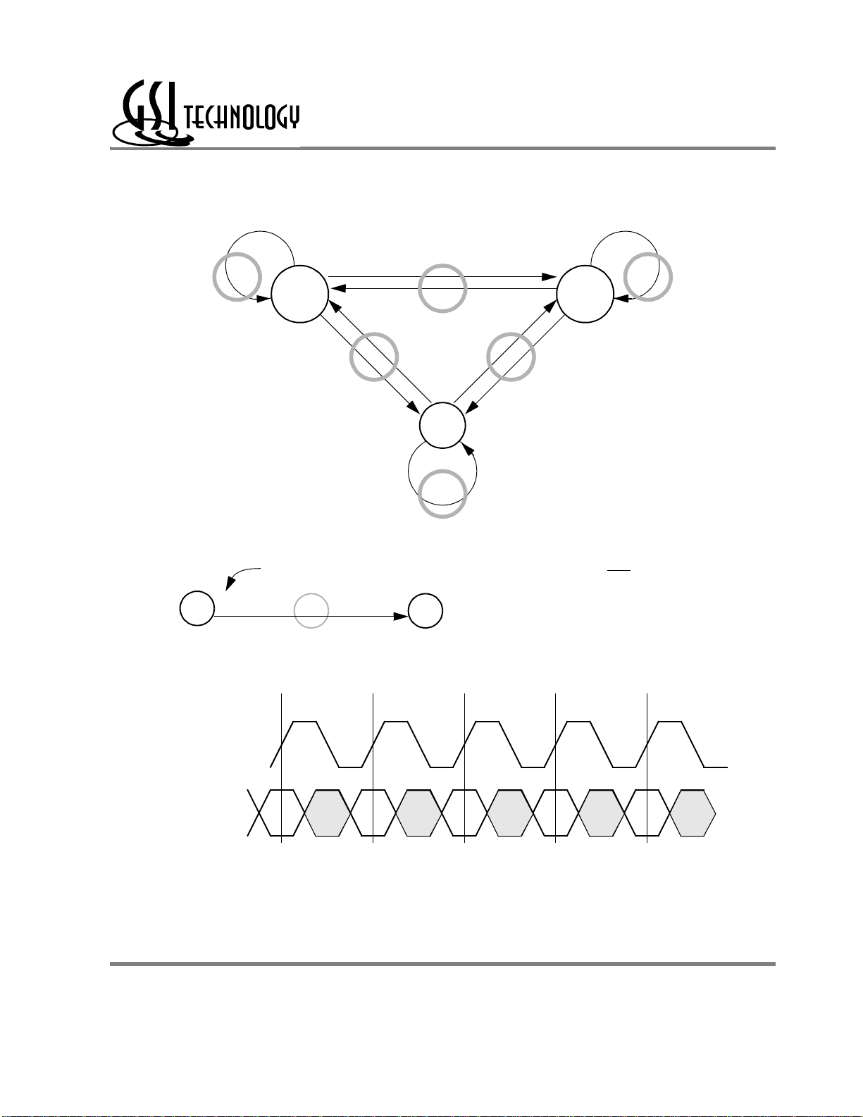
Pipeline and Flow Through Read-Write Control State Diagram
Preliminary.
GS881Z18/36T-11/100/80/66
D
B
Deselect
R
D
W
New Read New Write
R
B
R
W
W
R
R
Burst Read Burst Write
B
Key Notes
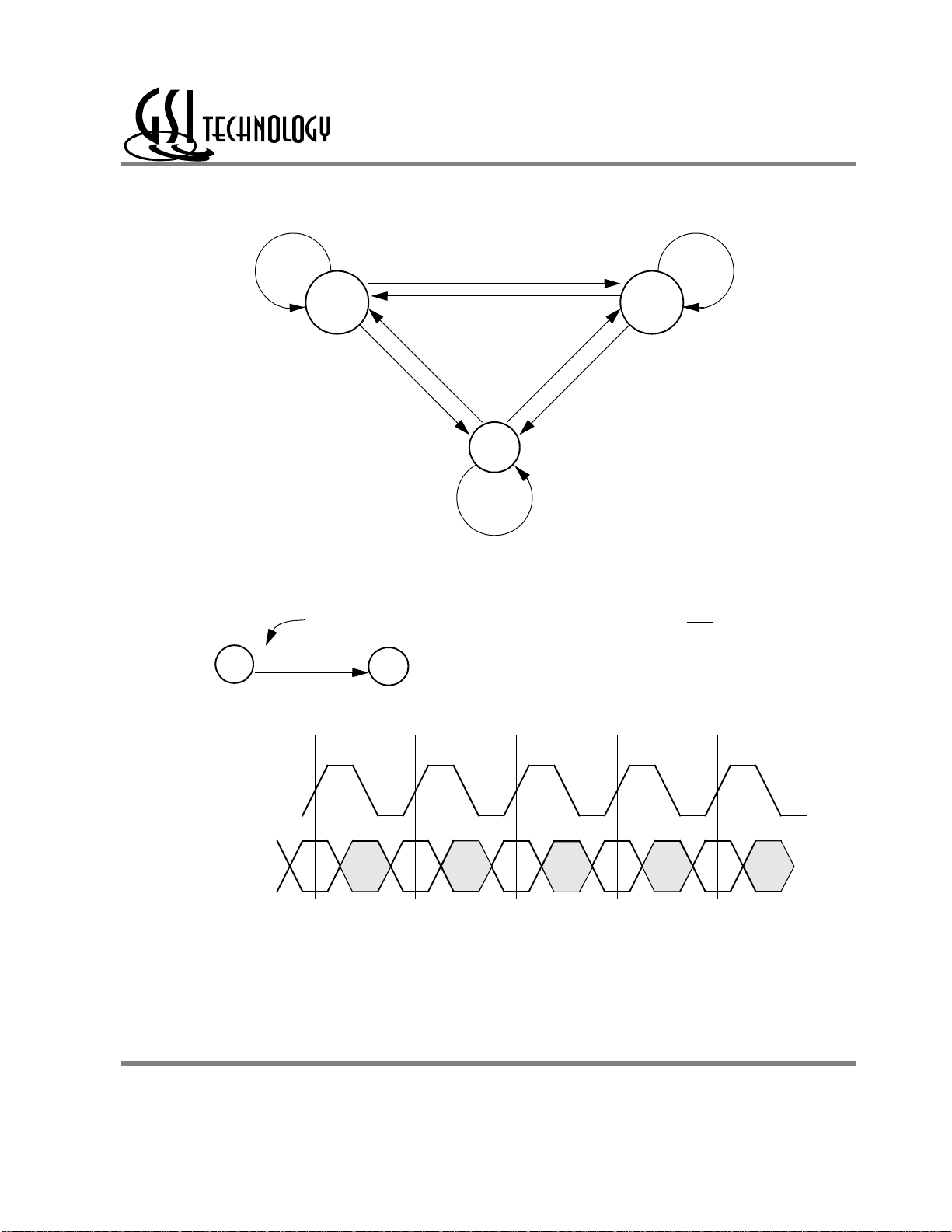
ƒ
Current State (n)
Input Command Code
Transition
Next State (n+1)
1. The Hold command (CKE Low) is not
shown because it prevents any state change.
2. W, R, B and D represent input command
codes, as indicated in the Synchronous Truth Table.
D
W
B
W
B
DD
n n+1 n+2 n+3
Clock (CK)
Command
Current State Next State
ƒ
ƒ ƒ ƒ
Current State and Next State Definition for Pipelined and Flow Through Read/Write Control State Diagram
Rev: 1.10 8/2000 9/34 © 1998, Giga Semiconductor, Inc.
Specifications cited are subject to change without notice. For latest documentation see http://www.gsitechnology.com
Pipeline Mode Data I/O State Diagram
Preliminary.
GS881Z18/36T-11/100/80/66
Intermediate Intermediate
Key
ƒ
Transition
Current State (n) Next State (n+2)
W
B
High Z
(Data In)
Input Command Code
Intermediate State (N+1)
R
D
Transition
Intermediate
Intermediate
W
High Z
B
D
Intermediate
R
B
Data Out
W
(Q Valid)
Intermediate
R
Notes
1. The Hold command (CKE Low) is not
shown because it prevents any state change.
2. W, R, B, and D represent input command
codes as indicated in the Truth Tables.
D
n n+1 n+2 n+3
Clock (CK)
Command
Current State
ƒ
ƒ ƒ ƒ
Intermediate
State
Next State
Current State and Next State Definition for Pipeline Mode Data I/O State Diagram
Rev: 1.10 8/2000 10/34 © 1998, Giga Semiconductor, Inc.
Specifications cited are subject to change without notice. For latest documentation see http://www.gsitechnology.com
Flow Through Mode Data I/O State Diagram
Preliminary.
GS881Z18/36T-11/100/80/66
W
B
High Z
(Data In)
Key Notes
Current State (n)
Input Command Code
ƒ
Transition
R
D
Next State (n+1)
W
R
High Z
B
D
1. The Hold command (CKE Low) is not
shown because it prevents any state change.
2. W, R, B, and D represent input command
codes as indicated in the Truth Tables.
R
B
Data Out
W
(Q Valid)
D
n n+1 n+2 n+3
Clock (CK)
Command
Current State Next State
ƒ
ƒ ƒ ƒ
Current State and Next State Definition for: Pipeline and Flow Through Read Write Control State Diagram
Rev: 1.10 8/2000 11/34 © 1998, Giga Semiconductor, Inc.
Specifications cited are subject to change without notice. For latest documentation see http://www.gsitechnology.com
 Loading...