


GS818QV36D-333I
GSI GS818QV36D-333I, GS818QV36D-333, GS818QV36D-300I, GS818QV36D-300, GS818QV36D-250I Datasheet
...
Rev: 1.01 11/2002 1/29
Specifications cited are design targets and are subject to change without notice. For latest documentation contact your GSI representative.
Preliminary
GS818QV18/36D-200/167/133
18Mb Σ2x2B2V
SigmaQuad SRAM
133 MHz–200 MHz
2.5 V V
DD
1.8 V and 1.5 V I/O
165-Bump BGA
Commercial Temp
Industrial Temp
Features
• Simultaneous Read and Write SigmaQuad™ Interface
• JEDEC-standard pinout and package
• Dual DoubleData Rate interface
• Echo Clock outputs track data output drivers
• Byte Write controls sampled at data-in time
• Burst of 2 Read and Write
• 1.5 V or 1.8 V HSTL Interface
• Pipelined read operation
• Fully coherent read and write pipelines
• ZQ mode pin for programmable output drive strength
• IEEE 1149.1 JTAG-compliant Boundary Scan
• 165-bump, 13 mm x 15 mm, 1 mm bump pitch BGA package
• Pin-compatible with future 36Mb, 72Mb, and 144Mb devices
SigmaRAM™ Family Overview
GS818QV18/36 are built in compliance with the SigmaQuad SRAM
pinout standard for Separate I/O synchronous SRAMs. They
are18,874,368-bit (18Mb) SRAMs. These are the first in a family of
wide, very low voltage HSTL I/O SRAMs designed to operate at the
speeds needed to implement economical high performance
networking systems.
SigmaQuad SRAMs are offered in a number of configurations. Some
emulate and enhance other synchronous separate I/O SRAMs. A
higher performance SDR (Single Data Rate) Burst of 2 versionis also
offered. The logical differences between the protocols employed by
these RAMs hinge mainly on various combinations of address
bursting, output data registering, and write cueing. Along with the
Common I/O family of SigmaRAMs, the SigmaQuad family of SRAMs
allows a user to implement the interface protocol best suited to the
task at hand.
Clocking and Addressing Schemes
A Σ2x2B2SigmaQuad SRAM is a synchronous device. It employs two
input register clock inputs, K and K
. K and K are independent singleended clock inputs, not differential inputs to a single differential clock
input buffer. The device also allows the user to manipulate the output
register clock inputs quasi independently with the C and C
clock
inputs. C and C
are also independent single-ended clock inputs, not
differential inputs. If the C clocks are tied high, the K clocks are routed
internally to fire the output registers instead. Each
Σ
2x2B2 igmaQuad
SRAM also supplies Echo Clock outputs, CQ and CQ
, that are
synchronized with read data output. When used in a source
synchronous clocking scheme, these Echo Clock outputs can be used
to fire input registers at the data’s destination.
Because Separate I/O
Σ
2x2B2 RAMs always transfer data in two
packets, A0 is internally set to 0 for the first read or write transfer, and
automatically incremented by 1 for the next transfer. Because the LSB
is tied off internally, the address field of a
Σ
2x2B2 RAM is always one
address pin less than the advertised index depth (e.g., the 1M x 18
has a 512K addressable index).
-200 -167 -133
tKHKH 5.0 ns 6.0 ns 7.5 ns
tKHQV 2.3 ns 2.5 ns 3.0 ns
165-Bump, 13 mm x 15 mm BGA
1 mm Bump Pitch, 11 x 15 Bump Array
Bottom View
JEDEC Std. MO-216, Variation CAB-1

Rev: 1.01 11/2002 2/29
Specifications cited are design targets and are subject to change without notice. For latest documentation contact your GSI representative.
Preliminary
GS818QV18/36D-200/167/133
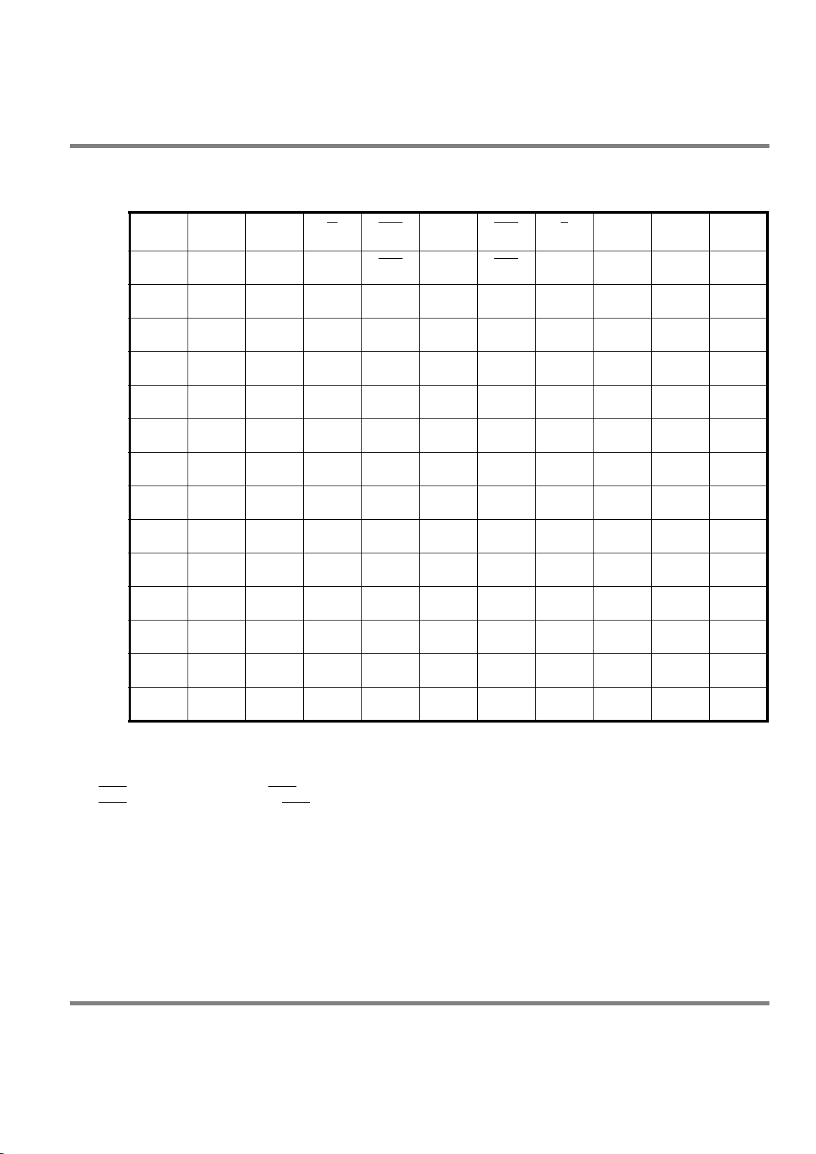
1M x 18 SigmaQuad SRAM — Top View
1234567891011
A CQ
MCL/SA
(144Mb)
NC/SA
(36Mb)
W
BW1 K NC R SA
MCL/SA
(72Mb)
CQ
B NC Q9 D9 SA NC K BW0
SA NC NC Q8
C NC NC D10 V
SS
SA
SA SA V
SS
NC Q7 D8
D NC D11 Q10 V
SS
V
SS
V
SS
V
SS
V
SS
NC NC D7
E NC NC Q11 V
DDQ
V
SS
V
SS
V
SS
V
DDQ
NC D6 Q6
F NC Q12 D12 V
DDQ
V
DD
V
SS
V
DD
V
DDQ
NC NC Q5
G NC D13 Q13 V
DDQ
V
DD
V
SS
V
DD
V
DDQ
NC NC D5
H NC V
REF
V
DDQ
V
DDQ
V
DD
V
SS
V
DD
V
DDQ
V
DDQ
V
REF
ZQ
J NC NC D14 V
DDQ
V
DD
V
SS
V
DD
V
DDQ
NC Q4 D4
K NC NC Q14 V
DDQ
V
DD
V
SS
V
DD
V
DDQ
NC D3 Q3
L NC Q15 D15 V
DDQ
V
SS
V
SS
V
SS
V
DDQ
NC NC Q2
M NC NC D16 V
SS
V
SS
V
SS
V
SS
V
SS
NC Q1 D2
N NC D17 Q16 V
SS
SA SA SA V
SS
NC NC D1
P NC NC Q17 SA SA C SA SA NC D0 Q0
R TDO TCK SA SA SA C
SA SA SA TMS TDI
11 x 15 Bump BGA—13 x 15 mm2 Body—1 mm Bump Pitch
Notes:
1. Expansion addresses: A3 for 36Mb, A10 for 72Mb, A2 for 144Mb
2. BW0
controls writes to D0:D8. BW1 controls writes to D9:D17.
3. MCL = Must Connect Low
4. It is recommended that H1 be tied low for compatibility with future devices.
Rev: 1.01 11/2002 3/29
Specifications cited are design targets and are subject to change without notice. For latest documentation contact your GSI representative.
Preliminary
GS818QV18/36D-200/167/133
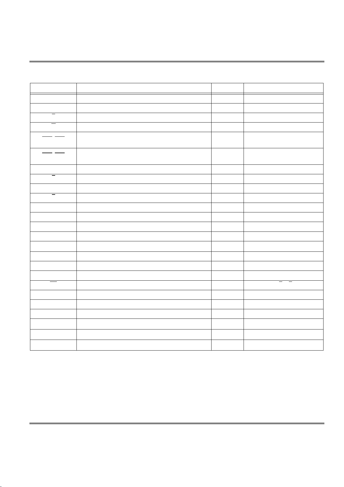
512K x 36 SigmaQuad SRAM — Top View
1234567891011
A
MCL/SA
(288Mb)
NC/SA
(72Mb)
W
BW2 BW1 R
NC/SA
(36Mb)
MCL/SA
(144Mb)
CQ
B Q27 Q18 D18 SA BW3
KBW0SA D17 Q17 Q8
C D27 Q28 D19 V
SS
SA
SA SA V
SS
D16 Q7 D8
D D28 D20 Q19 V
SS
V
SS
V
SS
V
SS
V
SS
Q16 D15 D7
E Q29 D29 Q20 V
DDQ
V
SS
V
SS
V
SS
V
DDQ
Q15 D6 Q6
F Q30 Q21 D21 V
DDQ
V
DD
V
SS
V
DD
V
DDQ
D14 Q14 Q5
G D30 D22 Q22 V
DDQ
V
DD
V
SS
V
DD
V
DDQ
Q13 D13 D5
H NC V
REF
V
DDQ
V
DDQ
V
DD
V
SS
V
DD
V
DDQ
V
DDQ
V
REF
ZQ
J D31 Q31 D23 V
DDQ
V
DD
V
SS
V
DD
V
DDQ
D12 Q4 D4
K Q32 D32 Q23 V
DDQ
V
DD
V
SS
V
DD
V
DDQ
Q12 D3 Q3
L Q33 Q24 D24 V
DDQ
V
SS
V
SS
V
SS
V
DDQ
D11 Q11 Q2
M D33 Q34 D25 V
SS
V
SS
V
SS
V
SS
V
SS
D10 Q1 D2
N D34 D26 Q25 V
SS
SA SA SA V
SS
Q10 D9 D1
P Q35 D35 Q26 SA SA C SA SA Q9 D0 Q0
R TDO TCK SA SA SA SA SA SA TMS TDI
11 x 15 Bump BGA—13 x 15 mm2 Body—1 mm Bump Pitch
Notes:
1. Expansion addresses: A9 for 36Mb, A3 for 72Mb, A10 for 144Mb, A2 for 288Mb
2. BW0
controls writes to D0:D8. BW1 controls writes to D9:D17.
3. BW2
controls writes to D18:D26. BW3 controls writes to D27:D35.
4. MCL = Must Connect Low
5. It is recommended that H1 be tied low for compatibility with future devices.
Rev: 1.01 11/2002 4/29
Specifications cited are design targets and are subject to change without notice. For latest documentation contact your GSI representative.
Preliminary
GS818QV18/36D-200/167/133
Note: NC = Not Connected to die or any other pin
Background
Separate I/O SRAMs, from a system architecture point of view, are attractive in applications where alternating reads and writes are needed.
Therefore, the SigmaQuad SRAM interface and truth table are optimized for alternating reads and writes. Separate I/O SRAMs are unpopular in
applications where multiple reads or multiple writes are needed because burst read or write transfers from Separate I/O SRAMs can cut the
RAM’s bandwidth in half.
Pin Description Table
Symbol Description Type Comments
SA Synchronous Address Inputs Input —
NC No Connect — —
R
Synchronous Read Input Active Low
W
Synchronous Write Input Active Low
BW0
–BW1 Synchronous Byte Writes Input
Active Low
x18 Version
BW0
–BW3 Synchronous Byte Writes Input
Active Low
x36 Version
K Input Clock Input Active High
K
Input Clock Input Active Low
C Output Clock Input Active High
C
Output Clock Input Active Low
TMS Test Mode Select Input —
TDI Test Data Input Input —
TCK Test Clock Input Input —
TDO Test Data Output Output —
V
REF
HSTL Input Reference Voltage Input —
ZQ Output Impedance Matching Input Input —
MCL Must Connect Low — —
CQ Synchronous Echo Clock Output Output Echoes C or K Clock
CQ
Synchronous Echo Clock-bar Output Output Echoes C or K Clock
Q0–Q35 Synchronous Data Outputs Output x36 Version
D0–D17 Synchronous Data Inputs Input x18 Version
Q0–Q17 Synchronous Data Outputs Output x18 Version
V
DD
Power Supply Supply 2.5 V Nominal
V
DDQ
Isolated Output Buffer Supply Supply 1.5 V Nominal
V
SS
Power Supply: Ground Supply —

Rev: 1.01 11/2002 5/29
Specifications cited are design targets and are subject to change without notice. For latest documentation contact your GSI representative.
Preliminary
GS818QV18/36D-200/167/133
A SigmaQuad SRAM can begin an alternating sequence of reads and writes with either a read or a write. In order for any separate I/O SRAM that
shares a common address between its two ports to keep both ports running all the time, the RAM must implement some sort of burst transfer
protocol. The burst must be at least long enough to cover the time the opposite port is receiving instructions on what to do next. The rate at which
a RAM can accept a new random address is the most fundamental performance metric for the RAM. Each of the three SigmaQuad SRAMs
support similar address rates because random address rate is determined by the internal performance of the RAM and they are all based on the
same internal circuits. Differences between the truth tables of the different SigmaQuad SRAMs, or any other Separate I/O SRAMs, follow from
differences in how the RAM’s interface is contrived to interact with the rest of the system. Each mode of operation has its own advantages and
disadvantages. The user should consider the nature of the work to be done by the RAM to evaluate which version is best suited to the application
at hand.
Alternating Read-Write Operations
SigmaQuad SRAMs follow a few simple rules of operation.
- Read or Write commands issued on one port are never allowed to interrupt an operation in progress on the other port.
- Read or Write data transfers in progress may not be interrupted and re-started.
- R
and W high always deselects the RAM but does not disable the CQ or CQ output pins.
- All address, data, and control inputs are sampled on clock edges.
In order to enforce these rules, each RAM combines present state information with command inputs. See the Truth Table for details.
Rev: 1.01 11/2002 6/29
Specifications cited are design targets and are subject to change without notice. For latest documentation contact your GSI representative.
Preliminary
GS818QV18/36D-200/167/133
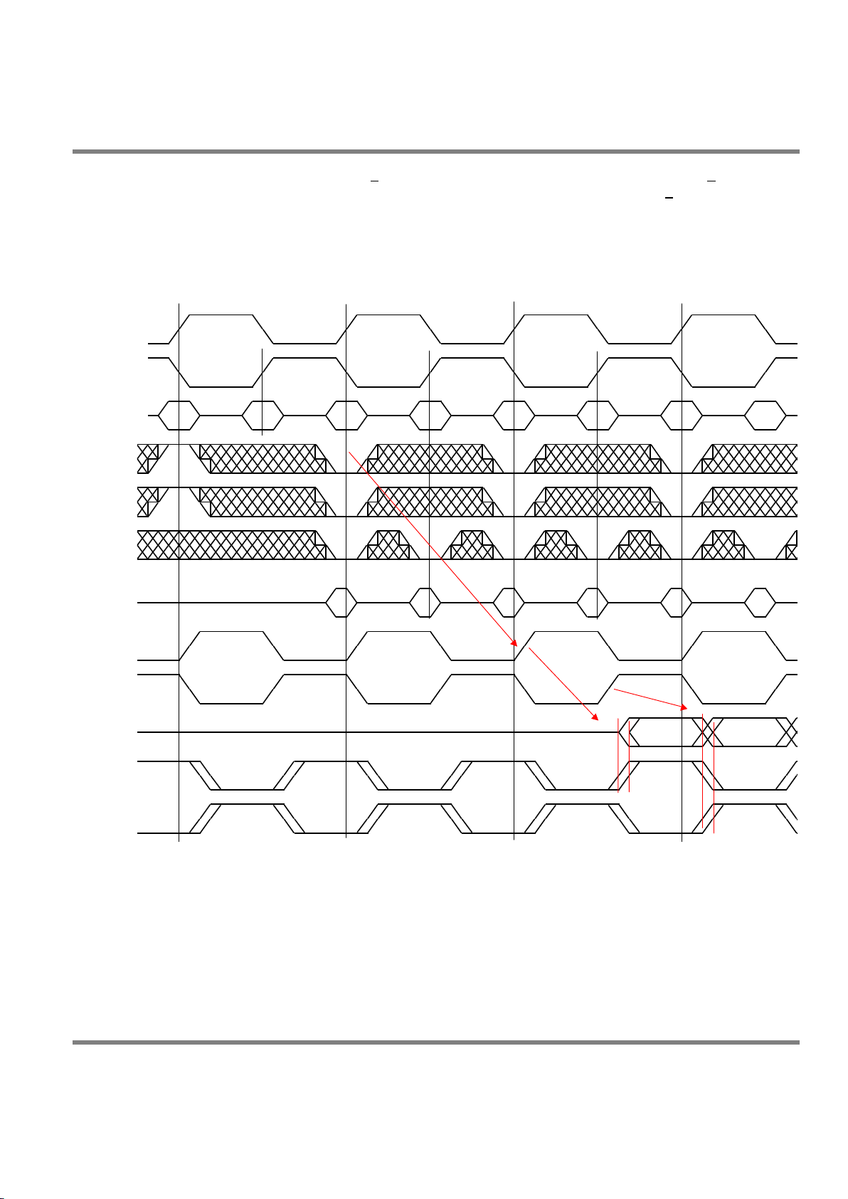
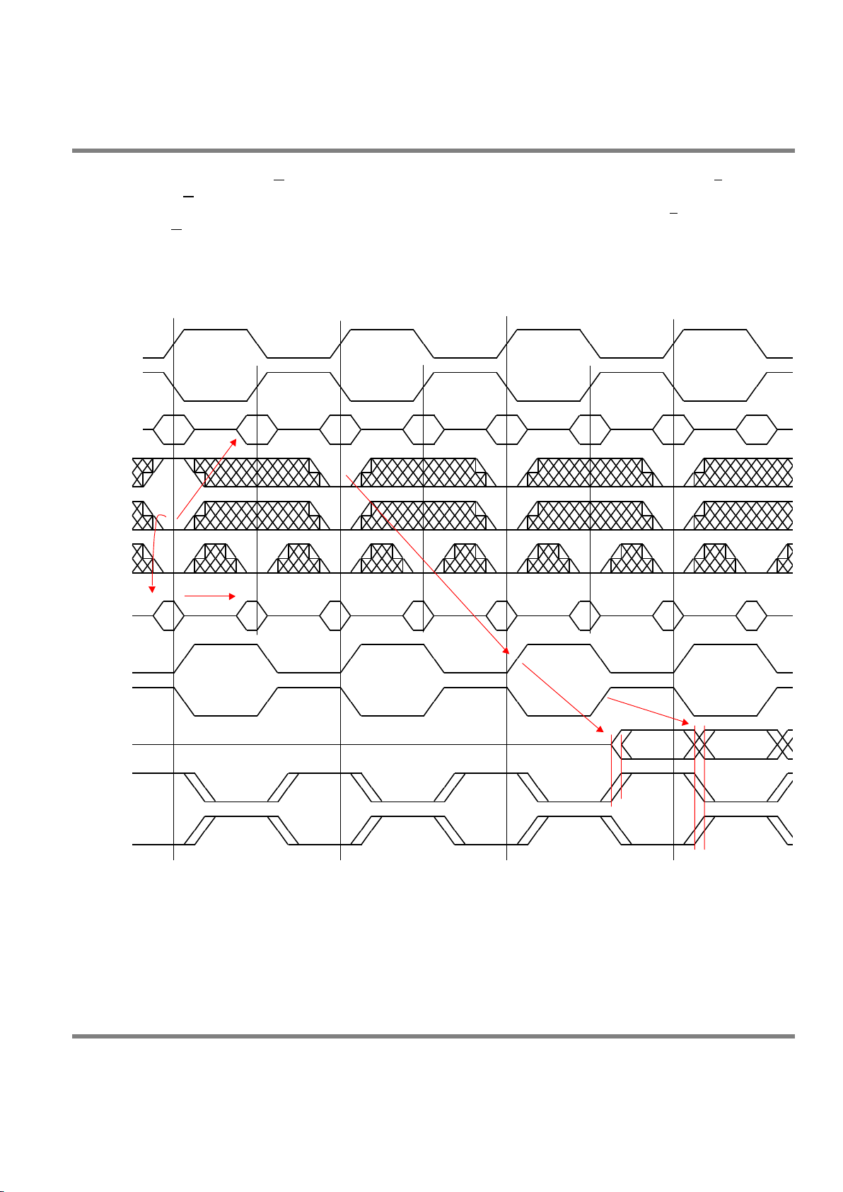
Σ
2x2B2 SigmaQuad SRAM DDR Read
The read port samples the status of the Address Input and R
pins at each rising edge of K. A low on the Read Enable-bar pin, R, begins a read
cycle. Data can be clocked out one cycle later and again one half cycle after that. A high on the Read Enable-bar pin, R
, begins a read port
deselect cycle.
Σ
2x2B2 Double Data Rate SigmaQuad SRAM Read First
Dwg Re v. G
DC0 DC1 DE0 DE1 DG0 DG1
Wri t eRead
GF
No Op
C
/C
CQ
D
Q
/R
/W
/BWx
/CQ
Wri t e
XX
K
/K
Address XX B C D
No Op Read Write Read
QB0 QB1
E
Rev: 1.01 11/2002 7/29
Specifications cited are design targets and are subject to change without notice. For latest documentation contact your GSI representative.
Preliminary
GS818QV18/36D-200/167/133
Σ
2x2B2 SigmaQuad SRAM DDR Write
The write port samples the status of the W
pin at each rising edge of K and the Address Input pins on the following rising edge of K. A low on the
Write Enable-bar pin, W
, begins a write cycle. The first of the data-in pairs associated with the write command is clocked in with the same rising
edge of K used to capture the write command. The second of the two data in transfers is captured on the rising edge of K
along with the write
address. A high on W
causes a write port deselect cycle.
Σ2x2B2 Double Data Rate SigmaQuad SRAM Write First
Dwg Re v. G
DB0 DB1 DD0 DD1 DF0 DF1 DH0 DH1
Wri t eRead
H
QC0 QC1
G
Wri t e Rea d Wr it e
C
/R
/W
/BWx
Read Write
AddressXXBCDE F
No Op
/C
CQ
/CQ
K
/K
D
Q
Rev: 1.01 11/2002 8/29
Specifications cited are design targets and are subject to change without notice. For latest documentation contact your GSI representative.
Preliminary
GS818QV18/36D-200/167/133
Special Functions
Byte Write Control
Byte Write Enable pins are sampled at the same time that Data In is sampled. A high on the Byte Write Enable pin associated with a particular
byte (e.g., BW0
controls D0–D8 inputs) will inhibit the storage of that particular byte, leaving whatever data may be stored at the current address
at that byte location undisturbed. Any or all of the Byte Write Enable pins may be driven high or low during the data in sample times in a write
sequence.
Each write enable command and write address loaded into the RAM provides the base address for a 2 beat data transfer. The x18 version of the
RAM, for example, may write 36 bits in association with each address loaded. Any 9-bit byte may be masked in any write sequence.
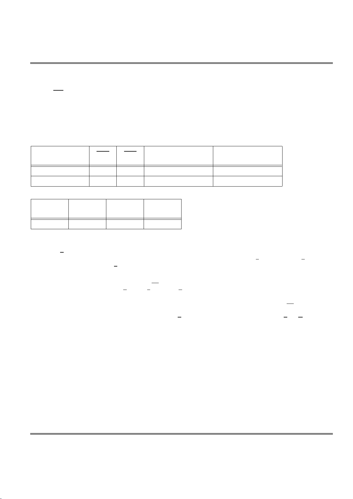
Example x18 RAM Write Sequence using Byte Write Enables
Resulting Write Operation
Output Register Control
SigmaQuad SRAMs offer two mechanisms for controlling the output data registers. Typically, control is handled by the Output Register Clock
inputs, C and C
. The Output Register Clock inputs can be used to make small phase adjustments in the firing of the output registers by allowing
the user to delay driving data out as much as a few nanoseconds beyond the next rising edges of the K and K
clocks. If the C and C clock inputs
are tied high, the RAM reverts to K and K
control of the outputs, allowing the RAM to function as a conventional pipelined read SRAM.
Echo Clock
SigmaQuad SRAMs feature Echo Clock outputs, CQ and CQ
, that track the performance of the output drivers. The Echo Clocks are delayed
copies of the Output Register clocks, C and C
or K and K (if the C and C clock inputs are tied high). Echo Clocks are designed to track changes
in output driver delays due to variance in die temperature and supply voltage. The Echo Clocks are designed to fire with the rest of the data
output drivers. SigmaQuad SRAMs provide both in-phase, or true, Echo Clock output, CQ and inverted Echo Clock output CQ
.
Echo Clocks are always active.
Neither inhibiting reads via holding R
high, nor deselection of the RAM via holding R and W high will
deactivate the Echo Clocks.
Data In Sample
Time
BW0 BW1 D0–D8 D9–D17
Beat 1 0 1 Data In Don’t Care
Beat 2 1 0 Don’t Care Data In
Byte 1
D0–D8
Byte 2
D9–D17
Byte 3
D0–D8
Byte 4
D9–D17
Written Unchanged Unchanged Written
Rev: 1.01 11/2002 9/29
Specifications cited are design targets and are subject to change without notice. For latest documentation contact your GSI representative.
Preliminary
GS818QV18/36D-200/167/133
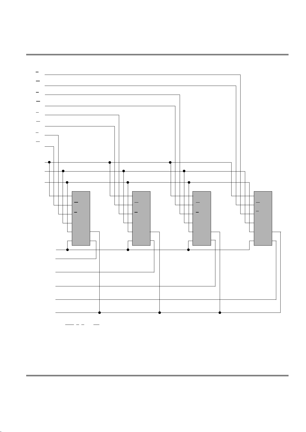
Example Four Bank Depth Expansion Schematic
A
K
R
W
A0–A
n
K
W
0
D1–D
n
Bank 0
Bank 1 Bank 2
Bank 3
R
0
CQ
D
A
K
W
CQ
D
A
K
W
CQ
D
A
K
W
CQ
D
R
R
R
QQQ Q
CC CC
Q1–Q
n
C
CQ
0
CQ
1
CQ
2
CQ
3
W
1
R
1
W
2
R
2
W
3
R
3
Note: For simplicity BWn, K, C and CQ are not shown.
 Loading...