


 Loading...
FUJITSU SEMICONDUCTOR |
CM25-10153-2E |
CONTROLLER MANUAL |
|
|
F2MC-8L
8-BIT MICROCONTROLLER
MB89202/F202RA Series
HARDWARE MANUAL

F2MC-8L
8-BIT MICROCONTROLLER
MB89202/F202RA Series
HARDWARE MANUAL
Be sure to refer to the “Check Sheet” for the latest cautions on development.
“Check Sheet” is seen at the following support page
URL:http://www.fujitsu.com/global/services/microelectronics/product/micom/support/index.html
“Check Sheet” lists the minimal requirement items to be checked to prevent problems beforehand in system development.
FUJITSU LIMITED
PREFACE
■ Purpose of This Manual and Intended Reader
The MB89202/F202RA series was developed as one of the general-purpose products of the
F2MC-8L family, which contains original 8-bit one-chip microcontrollers for use with ASICs (application specific ICs). The MB89202/F202RA series can be used in a wide range of products from consumer products to industrial products.
This manual explains the functions and operations of the MB89202/F202RA series for product development.
The F2MC-8L Programming Manual contains details of the programming instructions.
Note: F2MC, an abbreviation for FUJITSU Flexible Microcontroller, is a registered trademark of FUJITSU LIMITED.
■ Trademark
The company names and brand names herein are the trademarks or registered trademarks of their respective owners.
■ Structure of This Manual
This manual consists of the following 17 chapters and appendix.
CHAPTER 1 OVERVIEW
This chapter describes the features and basic specification of the MB89202/F202RA series.
CHAPTER 2 HANDLING DEVICES
This chapter describes the precautions to be taken when handling the MB89202/F202RA series.
CHAPTER 3 CPU
This chapter describes the functions and operation of the CPU.
CHAPTER 4 I/O PORTS
This chapter describes the functions and operation of the I/O ports.
CHAPTER 5 TIME-BASE TIMER
This chapter describes the functions and operation of the time-base timer.
CHAPTER 6 WATCHDOG TIMER
This chapter describes the functions and operation of the watchdog timer.
CHAPTER 7 8-BIT PWM TIMER
This chapter describes the functions and operation of the 8-bit PWM timer.
CHAPTER 8 8/16-BIT CAPTURE TIMER/COUNTER
This chapter describes the functions and operation of the 8/16-bit capture timer/counter.
CHAPTER 9 12-BIT PPG TIMER
This chapter describes the functions and operation of the 12-bit PPG timer.
i
CHAPTER 10 EXTERNAL INTERRUPT CIRCUIT 1 (EDGE)
This chapter describes the functions and operation of external interrupt circuit 1 (edge).
CHAPTER 11 EXTERNAL INTERRUPT CIRCUIT 2 (LEVEL)
This chapter describes the functions and operation of external interrupt circuit 2 (level).
CHAPTER 12 A/D CONVERTER
This chapter describes the functions and operation of the A/D converter.
CHAPTER 13 UART
This chapter describes the functions and operation of UART.
CHAPTER 14 8-BIT SERIAL I/O
This chapter describes the functions and operation of the 8-bit serial I/O.
CHAPTER 15 BUZZER OUTPUT
This chapter describes the functions and operation of the buzzer output.
CHAPTER 16 WILD REGISTER FUNCTIONS
This chapter describes the functions and operation of the wild registers.
CHAPTER 17 FLASH MEMORY
This chapter describes the functions and operation of the flash memory.
APPENDIX
This appendix shows the I/O map and instructions list.
ii

•The contents of this document are subject to change without notice. Customers are advised to consult with sales representatives before ordering.
•The information, such as descriptions of function and application circuit examples, in this document are presented solely for the purpose of reference to show examples of operations and uses of FUJITSU semiconductor device; FUJITSU does not warrant proper operation of the device with respect to use based on such information. When you develop equipment incorporating the device based on such information, you must assume any responsibility arising out of such use of the information. FUJITSU assumes no liability for any damages whatsoever arising out of the use of the information.
•Any information in this document, including descriptions of function and schematic diagrams, shall not be construed as license of the use or exercise of any intellectual property right, such as patent right or copyright, or any other right of FUJITSU or any third party or does FUJITSU warrant non-infringement of any third-party's intellectual property right or other right by using such information. FUJITSU assumes no liability for any infringement of the intellectual property rights or other rights of third parties which would result from the use of information contained herein.
•The products described in this document are designed, developed and manufactured as contemplated for general use, including without limitation, ordinary industrial use, general office use, personal use, and household use, but are not designed, developed and manufactured as contemplated (1) for use accompanying fatal risks or dangers that, unless extremely high safety is secured, could have a serious effect to the public, and could lead directly to death, personal injury, severe physical damage or other loss (i.e., nuclear reaction control in nuclear facility, aircraft flight control, air traffic control, mass transport control, medical life support system, missile launch control in weapon system), or (2) for use requiring extremely high reliability (i.e., submersible repeater and artificial satellite).
Please note that FUJITSU will not be liable against you and/or any third party for any claims or damages arising in connection with above-mentioned uses of the products.
•Any semiconductor devices have an inherent chance of failure. You must protect against injury, damage or loss from such failures by incorporating safety design measures into your facility and equipment such as redundancy, fire protection, and prevention of over-current levels and other abnormal operating conditions.
•Exportation/release of any products described in this document may require necessary procedures in accordance with the regulations of the Foreign Exchange and Foreign Trade Control Law of Japan and/or US export control laws.
•The company names and brand names herein are the trademarks or registered trademarks of their respective owners.
Copyright© 2005-2008 FUJITSU LIMITED All rights reserved
iii
READING THIS MANUAL
Example Notation of Register Names and Pin Names
Example notation of register names and bit names
By writing 1 into the sleep bit of the standby control register (STBC : SLP), ...
Bit name Register name Bit abbreviation
Register abbreviation
Prohibit the output of interrupt request of the time-base timer (TBTC : TBIE = 0).
Setting data
Bit abbreviation
Register abbreviation
If interrupt enabled (CCR : I = 1) is specified, the interrupt is accepted.
Current state
Bit abbreviation
Register abbreviation
Example notation of multi-use pins
P33/EC pin
Some pins can switch functions according to a setting made by a program or other method. These pins are called multi-use pins. For multi-use pins, the names corresponding to functions are listed and divided by /.
iv
CONTENTS
CHAPTER 1 |
OVERVIEW .......................................................................................... ......... |
1 |
|
1.1 |
Features of MB89202/F202RA Series ................................................................................................ |
2 |
|
1.2 |
MB89202/F202RA Series Product Lineup .......................................................................................... |
4 |
|
1.3 |
Differences between Models .............................................................................................................. |
6 |
|
1.4 |
Block Diagram of MB89202/F202RA Series ....................................................................................... |
7 |
|
1.5 |
Pin Assignment ................................................................................................................................... |
8 |
|
1.6 |
Package Dimensions ........................................................................................................................ |
10 |
|
1.7 |
Pin Functions Description ................................................................................................................. |
12 |
|
1.8 |
I/O Circuit Types ............................................................................................................................... |
14 |
|
CHAPTER 2 |
HANDLING DEVICES ....................................................................... ......... |
17 |
|
2.1 |
Precautions on Handling Devices ..................................................................................................... |
18 |
|
CHAPTER 3 |
CPU ................................................................................................... ......... |
21 |
|
3.1 |
Memory Space .................................................................................................................................. |
22 |
|
3.1.1 |
Specific-purpose Areas ............................................................................................................... |
24 |
|
3.1.2 |
Location of 16-bit Data on Memory ............................................................................................. |
26 |
|
3.2 |
Dedicated Register ........................................................................................................................... |
27 |
|
3.2.1 |
Condition Code Register (CCR) .................................................................................................. |
29 |
|
3.2.2 |
Register Bank Pointer (RP) ......................................................................................................... |
31 |
|
3.3 |
General-Purpose Registers .............................................................................................................. |
32 |
|
3.4 |
Interrupts ........................................................................................................................................... |
34 |
|
3.4.1 |
Interrupt Level Setting Registers (ILR1 to ILR4) .......................................................................... |
36 |
|
3.4.2 |
Steps in the Interrupt Operation .................................................................................................. |
37 |
|
3.4.3 |
Multiple Interrupts ........................................................................................................................ |
39 |
|
3.4.4 |
Interrupt Processing Time ........................................................................................................... |
40 |
|
3.4.5 |
Stack Operation at Interrupt Processing ...................................................................................... |
41 |
|
3.4.6 |
Stack Area for Interrupt Processing ............................................................................................. |
42 |
|
3.5 |
Reset |
...................................................................................................................... .......................... |
43 |
3.5.1 |
Reset Flag Register (RSFR) ........................................................................................................ |
45 |
|
3.5.2 |
External .......................................................................................................Reset Pin ................ |
47 |
|
3.5.3 |
Reset ..........................................................................................................................Operation |
48 |
|
3.5.4 |
State ..........................................................................................................of Each Pin at Reset |
50 |
|
3.6 |
Clock ................................................................................................................................................. |
|
51 |
3.6.1 |
Clock ..........................................................................................................................Generator |
53 |
|
3.6.2 |
Clock ...........................................................................................................................Controller |
54 |
|
3.6.3 |
System ......................................................................................Clock Control Register (SYCC) |
56 |
|
3.6.4 |
Clock ..................................................................................................................................Mode |
58 |
|
3.6.5 |
Oscillation ..............................................................................................Stabilization Wait Time |
60 |
|
3.7 |
Standby .............................................................................Mode (Low-Power Consumption Mode) |
62 |
|
3.7.1 |
Operations .......................................................................................................in Standby Mode |
63 |
|
3.7.2 |
Sleep .................................................................................................................................Mode |
64 |
|
3.7.3 |
Stop ...................................................................................................................................Mode |
65 |
|
|
|
v |
|
3.7.4 |
Standby Control Register (STBC) .......................................................................................... |
..... 66 |
|
3.7.5 |
Diagram for State Transition in Standby Mode ............................................................................ |
68 |
|
3.7.6 |
Notes on Standby Mode .............................................................................................................. |
70 |
|
3.8 |
Memory Access Mode ...................................................................................................................... |
72 |
|
CHAPTER 4 |
I/O PORTS ......................................................................................... ......... |
75 |
|
4.1 |
Overview of I/O Ports ........................................................................................................................ |
76 |
|
4.2 |
Port 0 |
..................................................................................................................... ........................... |
78 |
4.2.1 |
Registers of Port 0 (PDR0, DDR0, and PUL0) ............................................................................ |
80 |
|
4.2.2 |
Operations ...........................................................................................of Port 0 Functions ......... |
82 |
|
4.3 |
Port 3 ................................................................................................................................................ |
|
84 |
4.3.1 |
Registers ...................................................................................of Port 3 (PDR3, DDR3, PUL3) |
86 |
|
4.3.2 |
Operations ....................................................................................................of Port 3 Functions |
88 |
|
4.4 |
Port 4 ................................................................................................................................................ |
|
90 |
4.4.1 |
Registers ..........................................................................................................of Port 4 (PDR4) |
92 |
|
4.4.2 |
Operations ....................................................................................................of Port 4 Functions |
93 |
|
4.5 |
Port 5 ................................................................................................................................................ |
|
94 |
4.5.1 |
Registers ...................................................................................of Port 5 (PDR5, DDR5, PUL5) |
96 |
|
4.5.2 |
Operations ....................................................................................................of Port 5 Functions |
98 |
|
4.6 |
Port 6 .............................................................................................................................................. |
|
100 |
4.6.1 |
Registers .................................................................................of Port 6 (PDR6, DDR6, PUL6) |
103 |
|
4.6.2 |
Operations ..................................................................................................of Port 6 Functions |
105 |
|
4.7 |
Port 7 .............................................................................................................................................. |
|
107 |
4.7.1 |
Registers .................................................................................of Port 7 (PDR7, DDR7, PUL7) |
109 |
|
4.7.2 |
Operations ..................................................................................................of Port 7 Functions |
111 |
|
4.8 |
Programming ..................................................................................................Example of I/O Port |
113 |
|
CHAPTER 5 .................................................................................. |
TIME - BASE TIMER |
115 |
|
5.1 |
Overview .........................................................................................................of Time-base Timer |
116 |
|
5.2 |
Configuration ..................................................................................................of Time-base Timer |
118 |
|
5.3 |
Time-base .....................................................................................Timer Control Register (TBTC) |
119 |
|
5.4 |
Interrupt ..........................................................................................................of Time-base Timer |
121 |
|
5.5 |
Operations .....................................................................................of Time-base Timer Functions |
122 |
|
5.6 |
Notes ...................................................................................................on Using Time-base Timer |
124 |
|
5.7 |
Program ..........................................................................................Example for Time-base Timer |
125 |
|
CHAPTER 6 ................................................................................ |
WATCHDOG TIMER |
127 |
|
6.1 |
Overview .........................................................................................................of Watchdog Timer |
128 |
|
6.2 |
Configuration ...................................................................................................of Watchdog Timer |
129 |
|
6.3 |
Watchdog ..............................................................................................Control Register (WDTC) |
130 |
|
6.4 |
Operations ......................................................................................of Watchdog Timer Functions |
131 |
|
6.5 |
Notes ....................................................................................................on Using Watchdog Timer |
132 |
|
6.6 |
Program ..........................................................................................Example for Watchdog Timer |
133 |
|
vi
CHAPTER 7 8-BIT PWM TIMER ................................................................................... |
135 |
|
7.1 |
Overview of 8-bit PWM Timer ......................................................................................................... |
136 |
7.2 |
Configuration of 8-bit PWM Timer .................................................................................................. |
139 |
7.3 |
Pin of 8-bit PWM Timer ................................................................................................................... |
141 |
7.4 |
Registers of 8-bit PWM Timer ......................................................................................................... |
142 |
7.4.1 |
PWM Control Register (CNTR) ................................................................................................. |
143 |
7.4.2 |
PWM Compare Register (COMR) ............................................................................................. |
145 |
7.5 |
Interrupt of 8-bit PWM Timer .......................................................................................................... |
147 |
7.6 |
Operations of the Interval Timer Functions ..................................................................................... |
148 |
7.7 |
Operations of the 8-bit PWM Timer Functions ................................................................................ |
150 |
7.8 |
States in Each Mode During Operation .......................................................................................... |
152 |
7.9 |
Notes on Using 8-bit PWM Timer ................................................................................................... |
155 |
7.10 |
Program Example for PWM Timer .................................................................................................. |
157 |
CHAPTER 8 8/16-BIT CAPTURE TIMER/COUNTER ................................................... |
161 |
|
8.1 |
Overview of 8/16-bit Capture Timer/Counter .................................................................................. |
162 |
8.2 |
Configuration of 8/16-bit Capture Timer/Counter ............................................................................ |
166 |
8.3 |
Pins of 8/16-bit Capture Timer/Counter .......................................................................................... |
168 |
8.4 |
Registers of 8/16-bit Capture Timer/Counter .................................................................................. |
170 |
8.4.1 |
Capture Control Register (TCCR) ............................................................................................. |
171 |
8.4.2 |
Timer 0 Control Register (TCR0) ............................................................................................... |
173 |
8.4.3 |
Timer 1 Control Register (TCR1) ............................................................................................... |
175 |
8.4.4 |
Timer Output Control Register (TCR2) ...................................................................................... |
177 |
8.4.5 |
Timer 0 Data Register (TDR0) ................................................................................................... |
178 |
8.4.6 |
Timer 1 Data Register (TDR1) ................................................................................................... |
180 |
8.4.7 |
Capture Data Registers H and L (TCPH and TCPL) ................................................................. |
182 |
8.5 |
8/16-bit Capture Timer/Counter of Interrupts .................................................................................. |
183 |
8.6 |
Explanation of Operations of Interval Timer Functions ................................................................... |
185 |
8.7 |
Operation of Counter Functions ...................................................................................................... |
189 |
8.8 |
Functions of Operations of Capture Functions ............................................................................... |
193 |
8.9 |
8/16-bit Capture Timer/Counter Operation in Each Mode .............................................................. |
197 |
8.10 |
Notes on Using 8/16-bit Capture Timer/Counter ............................................................................ |
198 |
8.11 |
Program Example for 8/16-bit Capture Timer/Counter ................................................................... |
200 |
CHAPTER 9 12-BIT PPG TIMER .................................................................................. |
205 |
|
9.1 |
Overview of 12-bit PPG Timer ........................................................................................................ |
206 |
9.2 |
Configuration of 12-bit PPG Timer Circuit ...................................................................................... |
209 |
9.3 |
Pin of 12-bit PPG Timer .................................................................................................................. |
211 |
9.4 |
Registers of 12-bit PPG Timer ........................................................................................................ |
213 |
9.4.1 |
12-bit PPG Control Register 1 (RCR21) .................................................................................... |
214 |
9.4.2 |
12-bit PPG Control Register 2 (RCR22) .................................................................................... |
215 |
9.4.3 |
12-bit PPG Control Register 3 (RCR23) .................................................................................... |
216 |
9.4.4 |
12-bit PPG Control Register 4 (RCR24) .................................................................................... |
218 |
9.5 |
Operations of 12-bit PPG Timer Functions ..................................................................................... |
219 |
9.6 |
Notes on Using 12-bit PPG Timer .................................................................................................. |
221 |
9.7 |
Program Example for 12-bit PPG Timer ......................................................................................... |
223 |
vii
CHAPTER 10 EXTERNAL INTERRUPT CIRCUIT 1 (EDGE) ......................................... |
225 |
||
10.1 |
Overview of External Interrupt Circuit 1 .......................................................................................... |
226 |
|
10.2 |
Configuration of External Interrupt Circuit 1 .................................................................................... |
227 |
|
10.3 |
Pins of External Interrupt Circuit 1 .................................................................................................. |
229 |
|
10.4 |
Registers of External Interrupt Circuit 1 .......................................................................................... |
231 |
|
10.4.1 External Interrupt Control Register 1 (EIC1) .............................................................................. |
232 |
||
10.4.2 External Interrupt Control Register 2 (EIC2) .............................................................................. |
235 |
||
10.5 |
Interrupt of External Interrupt Circuit 1 ............................................................................................ |
237 |
|
10.6 |
Operations of External Interrupt Circuit 1 ....................................................................................... |
239 |
|
10.7 |
Program Example for External Interrupt Circuit 1 ........................................................................... |
241 |
|
CHAPTER 11 EXTERNAL INTERRUPT CIRCUIT 2 (LEVEL) ....................................... |
243 |
||
11.1 |
Overview of External Interrupt Circuit 2 .......................................................................................... |
244 |
|
11.2 |
Configuration of External Interrupt Circuit 2 .................................................................................... |
245 |
|
11.3 |
Pins of External Interrupt Circuit 2 .................................................................................................. |
246 |
|
11.4 |
Registers of External Interrupt Circuit 2 .......................................................................................... |
249 |
|
11.4.1 External Interrupt 2 Control Register (EIE2) .............................................................................. |
250 |
||
11.4.2 External Interrupt 2 Flag Register (EIF2) ................................................................................... |
252 |
||
11.5 |
Interrupt of External Interrupt Circuit 2 ............................................................................................ |
253 |
|
11.6 |
Operations of External Interrupt Circuit 2 ....................................................................................... |
254 |
|
11.7 |
Program Example for External Interrupt Circuit 2 ........................................................................... |
256 |
|
CHAPTER 12 |
A/D CONVERTER .................................................................................... |
259 |
|
12.1 |
Overview of A/D Converter ............................................................................................................. |
260 |
|
12.2 |
Configuration of A/D Converter ....................................................................................................... |
261 |
|
12.3 |
Pins of A/D Converter ..................................................................................................................... |
263 |
|
12.4 |
Registers of A/D Converter ............................................................................................................. |
265 |
|
12.4.1 A/D Control Register 1 (ADC1) .................................................................................................. |
266 |
||
12.4.2 A/D Control Register 2 (ADC2) .................................................................................................. |
268 |
||
12.4.3 A/D Data Register (ADDH and ADDL) ...................................................................................... |
270 |
||
12.4.4 A/D Enable Register (ADEN) ..................................................................................................... |
271 |
||
12.5 |
Interrupt of A/D Converter ............................................................................................................... |
272 |
|
12.6 |
Operations of A/D Converter Functions .......................................................................................... |
273 |
|
12.7 |
Notes on Using A/D Converter ....................................................................................................... |
275 |
|
12.8 |
Program Example for A/D Converter .............................................................................................. |
277 |
|
CHAPTER 13 |
UART ........................................................................................................ |
279 |
|
13.1 |
Overview of UART .......................................................................................................................... |
280 |
|
13.2 |
Configuration of UART .................................................................................................................... |
284 |
|
13.3 |
Pins of UART .................................................................................................................................. |
287 |
|
13.4 |
Registers of UART .......................................................................................................................... |
289 |
|
13.4.1 Serial Mode Control Register (SMC) ......................................................................................... |
290 |
||
13.4.2 Serial Rate Control Register (SRC) ........................................................................................... |
292 |
||
13.4.3 Serial Status and Data Register (SSD) ..................................................................................... |
294 |
||
13.4.4 Serial Input Data Register (SIDR) ............................................................................................. |
297 |
||
13.4.5 Serial Output Data Register (SODR) ......................................................................................... |
298 |
||
13.4.6 Clock Divider Selection Register (UPC) .................................................................................... |
299 |
||
|
|
viii |
|
13.4.7 Serial Switch Register (SSEL) ................................................................................................... |
301 |
|
13.5 |
Interrupt of UART ............................................................................................................................ |
303 |
13.6 |
Operations of UART Functions ....................................................................................................... |
304 |
13.6.1 Transmission Operations (Operating Mode 0, 1, 2, and 3) ....................................................... |
306 |
|
13.6.2 Reception Operations (Operating Mode 0, 1, or 3) ................................................................... |
307 |
|
13.6.3 Reception Operations (Operating Mode 2 Only) ....................................................................... |
309 |
|
13.7 |
Program Example for UART ........................................................................................................... |
311 |
CHAPTER 14 8-BIT SERIAL I/O ..................................................................................... |
313 |
|
14.1 |
Overview of 8-Bit Serial I/O ............................................................................................................ |
314 |
14.2 |
Configuration of 8-Bit Serial I/O ...................................................................................................... |
315 |
14.3 |
Pins of 8-Bit Serial I/O .................................................................................................................... |
317 |
14.4 |
Registers of 8-Bit Serial I/O ............................................................................................................ |
319 |
14.4.1 Serial Mode Register (SMR) ...................................................................................................... |
320 |
|
14.4.2 Serial Data Register (SDR) ....................................................................................................... |
323 |
|
14.5 |
Interrupt of 8-Bit Serial I/O .............................................................................................................. |
324 |
14.6 |
Operations of Serial Output Functions ............................................................................................ |
325 |
14.7 |
Operations of Serial Input Functions .............................................................................................. |
327 |
14.8 |
8-Bit Serial I/O Operation in Each Mode ......................................................................................... |
329 |
14.9 |
Notes on Using 8-Bit Serial I/O ....................................................................................................... |
333 |
14.10 |
Example of 8-Bit Serial I/O Connection .......................................................................................... |
334 |
14.11 |
Program Example for 8-Bit Serial I/O ............................................................................................. |
336 |
CHAPTER 15 BUZZER OUTPUT .................................................................................... |
339 |
|
15.1 |
Overview of the Buzzer Output ....................................................................................................... |
340 |
15.2 |
Configuration of the Buzzer Output ................................................................................................ |
341 |
15.3 |
Pin of the Buzzer Output ................................................................................................................. |
342 |
15.4 |
Buzzer Register (BZCR) ................................................................................................................. |
343 |
15.5 |
Program Example for Buzzer Output .............................................................................................. |
345 |
CHAPTER 16 WILD REGISTER FUNCTION .................................................................. |
347 |
|
16.1 |
Overview of the Wild Register Function .......................................................................................... |
348 |
16.2 |
Configuration of the Wild Register Function ................................................................................... |
349 |
16.3 |
Registers of the Wild Register Function ......................................................................................... |
350 |
16.3.1 Data Setting Registers (WRDR0 and WRDR1) ......................................................................... |
351 |
|
16.3.2 Higher Address Set Registers (WRARH0 and WRARH1) ......................................................... |
352 |
|
16.3.3 Lower Address Set Registers (WRARL0 and WRARL1) ........................................................... |
353 |
|
16.3.4 Address Comparison EN Register (WREN) .............................................................................. |
354 |
|
16.3.5 Data Test Set Register (WROR) ............................................................................................... |
355 |
|
16.4 |
Operations of the Wild Register Functions ..................................................................................... |
356 |
ix
CHAPTER 17 |
FLASH MEMORY ..................................................................................... |
357 |
|
17.1 |
Overview of Flash Memory ............................................................................................................. |
358 |
|
17.2 |
Flash Memory Control Status Register (FMCS) ............................................................................. |
359 |
|
17.3 |
Starting the Flash Memory Automatic Algorithm ............................................................................ |
361 |
|
17.4 |
Confirming the Automatic Algorithm Execution State ..................................................................... |
362 |
|
17.4.1 Data Polling Flag (DQ7) ............................................................................................................ |
363 |
||
17.4.2 Toggle Bit Flag (DQ6) ................................................................................................................ |
364 |
||
17.4.3 Timing Limit Exceeded Flag (DQ5) ........................................................................................... |
365 |
||
17.4.4 Toggle Bit-2 Flag (DQ2) ............................................................................................................ |
366 |
||
17.5 |
Detailed Explanation of Writing to Erasing Flash Memory .............................................................. |
367 |
|
17.5.1 Setting The Read/Reset State ................................................................................................... |
368 |
||
17.5.2 Writing Data ............................................................................................................................... |
369 |
||
17.5.3 Erasing All Data (Erasing Chips) ............................................................................................... |
371 |
||
17.6 |
Flash Security Feature .................................................................................................................... |
372 |
|
17.7 |
Notes on using Flash Memory ........................................................................................................ |
373 |
|
APPENDIX ...................................................................................................................... |
... |
375 |
|
APPENDIX A |
I/O Map ............................................................................................................................... |
376 |
|
APPENDIX B Overview of the Instructions ................................................................................................ |
380 |
||
B.1 |
Addressing ..................................................................................................................................... |
383 |
|
B.2 |
Special Instructions ........................................................................................................................ |
387 |
|
B.3 Bit Manipulation Instructions (SETB and CLRB) ............................................................................ |
391 |
||
B.4 |
F2MC-8L Instructions List ............................................................................................................... |
392 |
|
B.5 |
Instruction Map ............................................................................................................................... |
399 |
|
APPENDIX C Mask Options ...................................................................................................................... |
400 |
||
APPENDIX D Programming EPROM with Evaluation Chip ........................................................................ |
401 |
||
APPENDIX E Pin State of the MB89202/F202RA Series .......................................................................... |
402 |
||
INDEX |
................................................................................................................................... |
|
403 |
x
Main changes in this edition
Page |
|
|
Changes (For details, refer to main body.) |
|||
|
|
|
|
|||
- |
- |
|
The followings product name is changed. |
|||
|
|
|
(MB89202 →MB89202/F202RA) |
|||
|
|
|
|
|||
|
|
|
The followings term is changed. |
|||
|
|
|
(source oscillation →oscillation frequency) |
|||
|
|
|
|
|||
6 |
1.3 Differences between |
|
"Notes:" is changed. |
|||
|
Models |
|
(The followings sentence is deleted. |
|||
|
|
|
"• At turning on the power, when the device is used without inputting the external |
|||
|
|
|
reset, select "reset output supported" and "power-on reset supported" by mask |
|||
|
|
|
option.") |
|||
|
|
|
|
|||
|
|
|
The followings package is changed in Table 1.3-1. |
|||
|
|
|
(FPT-34P-M03 →FPT-32P-M03) |
|||
|
|
|
|
|
||
12 |
1.7 Pin Functions |
|
|
pin in Table 1.7-1 is changed. |
||
RST |
||||||
|
|
|
|
|
|
|
19 |
2.1 Precautions on |
|
"● External pull-up for the External Reset Pin |
|
of MB89F202/F202RA" is |
|
(RST) |
||||||
|
Handling Devices |
|
changed. |
|||
|
|
|
|
|||
24 |
3.1.1 Specific-purpose |
|
The summary is changed. |
|||
|
Areas |
|
|
|
|
|
|
|
"■ General-purpose Register Area (address: 0100H to 01FFH)" is changed. |
||||
|
|
|
||||
|
|
|
|
|||
|
|
|
"■ Vector Table Area (Address: FFC0H to FFFFH)" is changed. |
|||
|
|
|
|
|||
44 |
3.5 Reset |
|
"● Power-on reset" is changed. |
|||
|
|
|
|
|||
|
|
|
"Note:" is deleted. |
|||
|
|
|
|
|||
56 |
3.6.3 System Clock |
|
Figure 3.6-5 is changed. |
|||
|
Control Register (SYCC) |
|
|
|
|
|
57 |
|
Table 3.6-1 is changed. |
||||
|
|
|||||
|
|
|
|
|||
130 |
6.3 Watchdog Control |
|
Figure 6.3-1 is changed. |
|||
|
Register (WDTC) |
|
|
|
|
|
|
|
|
|
|||
186 |
8.6 Explanation of |
|
"● 8-bit mode"is changed. |
|||
|
Operations of Interval |
|
(The followings sentence is deleted. |
|||
|
Timer Functions |
|
"The initial value of the square wave output is "L" level. The square wave output is |
|||
|
|
|
initialized by writing "0" to the TSTR bit of the timer control register (TCR).") |
|||
|
|
|
|
|||
264 |
12.3 Pins of A/D |
|
"■ Block Diagram of the Pins Related to the A/D Converter" is changed. |
|||
|
Converter |
|
("Note:" is deleted.) |
|||
|
|
|
|
|||
308 |
13.6.2 Reception |
|
"■ Reception Operations (Operating Mode 0, 1, or 3)" is changed. |
|||
|
Operations (Operating |
|
("Note:" is changed.) |
|||
|
Mode 0, 1, or 3) |
|
|
|
|
|
|
|
|
|
|
|
|
xi
Page |
|
Changes (For details, refer to main body.) |
||
|
|
|
||
310 |
13.6.3 Reception |
"■ Reception Operations (Operating Mode 2 Only)" is changed. |
||
|
Operations (Operating |
("Note:" is changed.) |
||
|
Mode 2 Only) |
|
|
|
|
|
|
|
|
358 |
17.1 Overview of Flash |
"■ High voltage supply on |
|
pin (applicable to MB89F202RA only)" is added. |
RST |
||||
|
Memory |
|
|
|
|
|
|
||
370 |
17.5.2 Writing Data |
Figure 17.5-1 is changed. |
||
|
|
(F555 →F554) |
||
|
|
|
||
394 |
B.4 F2MC-8L |
Table B.4-2 is changed. |
||
|
Instructions List |
("No.22 DECW A" is changed.) |
||
|
|
|
|
|
The vertical lines marked in the left side of the page show the changes.
xii

CHAPTER 1
OVERVIEW
This chapter describes the features and basic specification of the MB89202/F202RA series.
1.1Features of MB89202/F202RA Series
1.2MB89202/F202RA Series Product Lineup
1.3Differences between Models
1.4Block Diagram of MB89202/F202RA Series
1.5Pin Assignment
1.6Package Dimensions
1.7Pin Functions Description
1.8I/O Circuit Types
1

CHAPTER 1 OVERVIEW
1.1Features of MB89202/F202RA Series
The MB89202/F202RA series contains general-purpose single-chip microcontrollers that incorporate a full range of peripheral functions such as A/D converter, UART, PWM timer, PPG, capture timer/counter and external interrupts as well as a compact instruction set.
■Features of MB89202/F202RA Series
●F2MC-8L CPU core
•Instruction set most suitable for controllers
•Multiplication and division instruction
•16-bit operation
•Branch instruction by bit test
•Bit operation instruction, and others
●4-system timers
•8/16-bit capture timer/counter (8-bit capture timer/counter + 8-bit timer or 16-bit capture timer/counter)
•8-bit PWM timer (also available as an interval timer)
•21-bit time-base timer
•Watchdog timer
●10-bit A/D converter
•10-bit A/D × 8 channels
•Activation by 8/16-bit capture timer/counter output is possible.
●Programmable pulse generator (PPG)
•Pulse width and cycle are software selectable (12-bit PPG).
●UART
•6, 7, or 8 transfer data length
●8-bit serial I/O
•Available when switched from UART
•LSB first/MSB first selectability
●External interrupts
•External interrupt 1 (edge detection × 3 pins) has three independent inputs and can be used for wake-up from low-power consumption mode. (The edge detection can be selected from rising-edge, falling-edge, and both-edge modes.)
2
CHAPTER 1 OVERVIEW
•External interrupt 2 (level detection × 8 pins, 1 channel) has eight independent inputs and can be used for wake-up from low-power consumption mode. (L level detection function is supported.)
●Low-power consumption modes (standby modes)
•Stop mode (The oscillation is stopped so that current consumption is minimal.)
•Sleep mode (The CPU is stopped so that the current consumption is reduced by one-third of normal consumption.)
●Up to 26 pins of I/O ports
•General-purpose I/O ports (CMOS): 26 pins (4 of which can be used as N-ch open-drain I/O ports.)
●Wild registers
•2-byte data at two addresses are available.
•When a specific address or data is used on a wild register, the data in the ROM area is changed.
●16 KB Flash with read protection
•Once the protection code is written in the specified address, the FLASH content cannot be read by parallel/serial programmer.
3

CHAPTER 1 OVERVIEW
1.2MB89202/F202RA Series Product Lineup
Four MB89202 series models are available. Table 1.2-1 shows the models and Table 1.2- 2 shows the CPU and peripheral functions.
■ MB89202/F202RA Series Models
Table 1.2-1 MB89202/F202RA Series Models
|
MB89201 |
MB89F202/F202RA |
MB89V201 |
|
|
|
|
|
|
Classification |
Evaluation product |
Flash memory product |
Mask ROM product |
|
(for development) |
(read protection) |
|
||
|
|
|||
|
|
|
|
|
ROM size |
32K × 8 bits |
16K × 8 bits |
16K × 8 bits |
|
(External EPROM*2) |
(Internal Flash) |
(Internal mask ROM) |
||
|
||||
RAM size |
|
512 × 8 bits |
|
|
|
|
|
|
|
Low-power consumption |
|
Sleep mode and stop mode |
|
|
(standby mode) |
|
|
|
|
|
|
|
|
|
Process |
|
CMOS |
|
|
|
|
|
|
|
Operating voltage*1 |
2.7V to 5.5V |
3.5V to 5.5V |
2.2V to 5.5V |
*1: The minimum operating voltage varies with conditions such as operating frequency, functions, and connecting ICE.
*2: MBM27C256A is used as the external ROM.
4
CHAPTER 1 OVERVIEW
Table 1.2-2 CPU and Peripheral Functions of MB89202/F202RA Series
Item |
|
Specification |
||
|
|
|
|
|
|
|
Number of basic instructions: |
136 instructions |
|
|
|
Instruction bit length: |
8 bits |
|
CPU function |
Instruction length: |
1 to 3 bytes |
||
Data bit length: |
1, 8, or 16 bits |
|||
|
|
|||
|
|
Minimum instruction execution time: 0.32 to 5.1 µs (at 12.5 MHz) |
||
|
|
Interrupt processing time: |
2.88 to 46.1 µs (at 12.5 MHz) |
|
|
|
|
||
|
Port |
General-purpose I/O port: 26 pins (Also serve as peripherals. 4 of which can be used as N-ch |
||
|
open-drain I/O ports.) |
|||
|
|
|||
|
|
|
|
|
|
21-bit |
21 bits |
|
|
|
time-base |
Interrupt cycle: 0.66 ms, 2.64 ms, 21 ms, or 335.5 ms with 12.5MHz main clock |
||
|
timer |
|
|
|
|
|
|
||
|
Watchdog |
Reset occurrence cycle: When the main clock is at 12.5 MHz (minimum 335.5 ms) |
||
|
timer |
|
|
|
|
|
|
||
|
8-bit |
8-bit interval timer operation (Square wave output is supported. Operating clock cycle: |
||
|
1 tINST, 16 tINST, 64 tINST, and 8/16-bit capture timer/counter output) |
|||
|
PWM |
|||
|
8-bit resolution PWM operation (Conversion cycle: |
|||
|
timer |
|||
|
256 tINST, 4096 tINST, 16384 tINST and 256 times 8/16-bit capture timer/counter output) |
|||
|
|
|||
|
8/16-bit |
8-bit capture timer/counter × 1 channel + 8-bit timer or 16-bit capture timer/counter × 1 channel |
||
|
capture |
When timer 0 or a 16-bit counter is operating, event-counting operation by external clock input |
||
|
timer/ |
and square wave output are supported. |
|
|
|
counter |
|
|
|
|
|
|
|
|
Periphera |
UART |
Transfer data length: 6, 7, or 8 bits |
|
|
|
|
|
||
l function |
8-bit serial |
8 bits length, LSB first/MSB first selectability |
||
|
||||
|
One clock selectable from four operation clocks |
|||
|
I/O |
|||
|
(one external shift clock, three internal shift clocks: 2 tINST, 8 tINST, 32 tINST) |
|||
|
|
|||
|
12-bit |
Output frequency: Pulse width and cycle are selectable. |
||
|
PPG timer |
|
|
|
|
|
|
||
|
External |
3 channels (interrupt vector, request flag, and request output enable) |
||
|
interrupt 1 |
Edge selectability (selectable from rising edge, falling edge, and both-edge modes) |
||
|
(wake-up) |
Also available for wake-up from stop or sleep (Edge detection is also available in stop mode.) |
||
|
|
|
||
|
External |
8 inputs 1 channel (L level interrupt and input enable are independent.) |
||
|
interrupt 2 |
Also available for wake-up from stop or sleep (Level detection is also available in stop mode.) |
||
|
(wake-up) |
|
|
|
|
|
|
|
|
|
10-bit A/D |
10-bit resolution × 8 channels |
|
|
|
A/D conversion function (Conversion time: 38 tINST) |
|||
|
converter |
|||
|
Continuous activation by 8/16-bit capture timer/counter output or time-base timer output. |
|||
|
|
|||
|
|
|
|
|
|
Wild |
8-bit × 2 |
|
|
|
register |
|
|
|
|
|
|
|
|
Note:
The oscillation is 12.5 MHz unless another condition such as the main clock maximum speed, the clock
cycle value, or conversion time is stated.
5
CHAPTER 1 OVERVIEW
1.3Differences between Models
This section describes the precautions to be taken when selecting a MB89202/F202RA series model.
■ Precautions when Selecting a Model
Table 1.3-1 Differences between Models
Package |
MB89201 |
MB89F202/F202RA |
MB89V202 |
DIP-32P-M06
FPT-32P-M03
FPT-64P-M03
●Current consumption
•When operated at a low speed, the current consumption of a model with a flash is greater than that of a model with a mask ROM, though the current consumption in sleep or stop mode is the same.
Notes:
•For details on each package, see Section "1.6 Package Dimensions ".
•For details on current consumption and electrical characteristics of A/D converter, see the electrical characteristics in the Data Sheet.
6
CHAPTER 1 OVERVIEW
1.4Block Diagram of MB89202/F202RA Series
Figure 1.4-1 shows the block diagram of the MB89202/F202RA series.
■ Block Diagram of MB89202/F202RA Series
Figure 1.4-1 Block Diagram of MB89202/F202RA Series
X0
Main clock
X1 oscillator
Clock controller
RST |
6 |
Reset circuit |
|
Port |
|
|
2 |
|
P60, P61 |
|
CMOS I/O port |
|
|
*1P70 |
3 |
|
7 |
|
|
to |
|
|
|
Port |
CMOS I/O port |
|
|
|
|
||
1 |
P72 |
|
|
||
* |
|
|
|||
P04 / INT24 |
4 |
|
CMOS I/O port |
|
to |
|
|
|
|
P07 / INT27 |
|
|
|
|
|
2 |
8 |
External |
|
P02 / INT22 / AN6, |
interrupt2 |
|||
|
||||
P03 / INT23 / AN7 |
|
0 |
(wake-up) |
|
|
|
|||
|
2 |
Port |
|
|
P00 / INT20 / AN4, |
4 |
|
||
P01 / INT21 / AN5 |
|
|
|
|
|
|
4 |
10-bit A/D |
|
|
|
|
converter |
|
*1P40 / AN0 |
4 |
4 |
|
|
*1P43 / AN3 |
|
Port |
|
|
to |
|
|
|
|
|
|
|
CMOS I/O port |
|
|
|
|
(N-ch OD) |
|
|
|
|
*2 |
|
|
|
512 or 256 bytes RAM |
||
|
|
|
|
F2MC - 8 L CPU |
|
|
Other pins |
|
|
|
|
|
|
||||
|
|
|
|
|
|
|
|
|
|
|
|
|
VCC, VSS, C |
|
*2 |
||
|
|
16K or 8K bytes ROM |
|||
|
|
|
|
||
|
|
|
|
|
|
|
|
|
|
|
|
|
|
|
|
|
|
|
|
|
|
Wild register |
|
|
|
|
|
|
|

 Time-base timer
|
CMOS I/O port |
|
|
|
8-bit PWM |
Port 5 |
P50 / PWM |
buslaIntern |
UART prescaler |
witchingsnction |
|
UART |
P32 / UI / SI |
||
|
|
|
|
|
|
|
P30 / UCK / SCK |
|
|
|
P31 / UO / SO |
|
8-bit |
al fu |
|
|
serial I/O |
eri |
|
|
|
S |
|
|
8/16-bit |
|
P33 / EC |
|
|
|
|
|
capture timer/ |
3 |
P34 / TO / INT10 |
|
counter |
Port |
|
|
|
||
|
|
|
|
|
|
3 |
P35 / INT11 |
|
External interrupt1 |
||
|
P36 / INT12 |
||
|
|
|
|
|
12-bit PPG |
|
|
|
|
|
P37 / BZ / PPG |
|
Buzzer output |
|
|
|
CMOS I/O port |
|
|
*1: Large-current drive type
*2 : Check section "3.1 Memory Space"
7

CHAPTER 1 OVERVIEW
1.5Pin Assignment
Figure 1.5-1 and Figure 1.5-2 show the pin assignment of the MB89202/F202RA series.
■ Pin Assignment of DIP-32P-M06
Figure 1.5-1 Pin Assignment of DIP-32P-M06
|
|
|
|
|
|
1 |
|
|
|
VCC |
|||
P04/INT24 |
|
32 |
|
|
|||||||||
|
|
|
|||||||||||
|
|
|
|
|
|
|
|
|
|
|
|
|
|
P05/INT25 |
|
|
|
2 |
31 |
|
|
P03 |
/INT23 |
/AN7 |
|||
|
|
||||||||||||
|
|
|
|
|
|
3 |
|
|
|
|
|
|
|
P06/INT26 |
|
|
|
30 |
|
|
P02/INT22/AN6 |
||||||
|
|
||||||||||||
|
|
|
|
|
|
|
|
|
|
|
|
|
|
P07/INT27 |
|
|
|
4 |
29 |
|
|
P01/INT21/AN5 |
|||||
|
|
||||||||||||
|
|
P60 |
|
5 |
28 |
|
|
|
|
|
|
||
|
|
|
|
|
P00/INT20/AN4 |
||||||||
|
|
||||||||||||
|
|
P61 |
|
6 |
27 |
|
|
P43/AN3* |
|||||
|
|
||||||||||||
|
|
|
|
7 |
26 |
|
|
P42/AN2* |
|||||
|
|
RST |
|
|
|
|
|
||||||
|
|
||||||||||||
|
|
X0 |
|
8 |
25 |
|
|
P41/AN1* |
|||||
|
|
||||||||||||
|
|
X1 |
|
9 |
24 |
|
|
P40/AN0* |
|||||
|
|
||||||||||||
|
|
VSS |
|
10 |
23 |
|
|
P72* |
|||||
|
|
||||||||||||
P37/BZ/PPG |
|
11 |
22 |
|
|
P71* |
|||||||
|
|
||||||||||||
P36/INT12 |
|
12 |
21 |
|
|
P70* |
|||||||
|
|
||||||||||||
P35/INT11 |
|
13 |
20 |
|
|
P50/PWM |
|||||||
|
|
||||||||||||
P34/TO/INT10 |
|
14 |
19 |
|
|
P30/UCK/SCK |
|||||||
|
|
||||||||||||
P33/EC |
|
15 |
18 |
|
|
P31/UO/SO |
|||||||
|
|
||||||||||||
|
|
C |
|
|
16 |
17 |
|
|
P32/UI/SI |
||||
|
|
|
|
|
|
||||||||
|
|
|
|
|
|
|
|
|
|
|
|
|
|
* : Large-current drive type
8
CHAPTER 1 OVERVIEW
■ Pin Assignment of FPT-34P-M03
Figure 1.5-2 Pin Assignment of FPT-34P-M03
P04/INT24 |
|
1 |
34 |
|
VCC |
|
|
||||
P05/INT25 |
|
2 |
33 |
|
P03/INT23/AN7 |
|
|
||||
P06/INT26 |
|
3 |
32 |
|
P02/INT22/AN6 |
|
|
||||
|
|
4 |
31 |
|
|
P07/INT27 |
|
|
P01/INT21/AN5 |
||
|
|
5 |
30 |
|
P00/INT20/AN4 |
P60 |
|
|
|||
|
|
6 |
29 |
|
P43/AN3 * |
P61 |
|
|
|||
|
|
|
|
|
P42/AN2 * |
RST |
|
7 |
28 |
|
|
|
|
|
|
|
P41/AN1 * |
X0 |
|
8 |
27 |
|
|
|
|
|
|
|
P40/AN0 * |
X1 |
|
9 |
26 |
|
|
|
|
|
|
|
P72* |
VSS |
|
10 |
25 |
|
|
|
|
|
|
|
P71 * |
P37/BZ/PPG |
|
11 |
24 |
|
|
|
|
|
|
|
P70 * |
P36/INT12 |
|
12 |
23 |
|
|
|
|
|
|
|
|
P35/INT11 |
|
13 |
22 |
|
N.C. |
|
|
|
|
P50/PWM |
|
P34/TO/INT10 |
|
14 |
21 |
|
|
|
|
|
|
|
|
P33/EC |
|
15 |
20 |
|
P30/UCK/SCK |
|
|
|
|
|
|
N.C. |
|
16 |
19 |
|
P31/UO/SO |
|
|
||||
|
|
|
|
|
P32/UI/SI |
C |
|
17 |
18 |
|
|
|
|
|
|
|
|
* : Large-current drive type
Note: N.C.: Do not use because it is connected internally.
9

CHAPTER 1 OVERVIEW
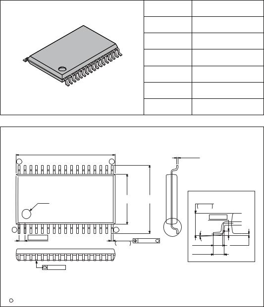
1.6Package Dimensions
Two different packages are available for MB89202/F202RA series. Figure 1.6-1 and Figure 1.6-2 show package dimensions.
■ Package Dimension of DIP-32P-M06 |
|
|
Figure 1.6-1 Package Dimension of DIP-32P-M06 |
|
|
32-pin plastic SH-DIP |
Lead pitch |
1.778 mm |
|
Low space |
10.16 mm |
|
Sealing method |
Plastic mold |
(DIP-32P-M06) |
|
|
32-pin plastic SH-DIP |
Note 1) * : These dimensions do not include resin protrusion. |
||
(DIP-32P-M06) |
Note 2) Pins width and pins thickness include plating thickness. |
||
|
*28.00 |
+0.20 |
|
|
–0.30 |
|
|
|
1.102 |
+.008 |
|
|
–.012 |
|
|
|
|
|
|
INDEX
*8.89±0.25 (.350±.010)
|
|
|
1.02 |
+0.30 |
|
|
|
|
|
|
|
|
–0.20 |
|
|
|
|
||
|
|
|
.040 |
+.012 |
|
|
|
|
|
|
|
|
–.008 |
|
|
|
|
||
4.70 –0.20+0.70 |
|
|
|
|
|
0.51(.020) |
|
|
|
|
+.028 |
|
|
|
|
|
|
|
|
.185 |
|
|
|
|
|
MIN. |
|
|
|
–.008 |
|
|
|
|
|
|
|
||
3.30 |
+0.20 |
|
|
|
|
|
|
|
|
–0.30 |
|
|
|
|
|
|
|
|
|
.130 |
+.008 |
|
|
|
|
|
|
|
|
–.012 |
|
|
|
|
|
|
+0.03 |
|
|
|
|
|
|
|
|
|
0.27 |
|
|
|
|
|
|
|
|
|
–0.07 |
|
|
|
|
|
|
|
|
|
.011 |
+.001 |
10.16(.400) |
|
|
1.778(.070) |
|
+0.08 |
|
–.003 |
|||
|
1.27(.050) |
0.48 |
|
|
|
|
|||
|
–0.12 |
0.25(.010) |
M |
|
0~15˚ |
||||
|
MAX. |
|
|
+.003 |
|
||||
|
|
.019–.005 |
|
|
|
|
|||
|
Dimensions in mm (inches). |
C 2003 FUJITSU LIMITED D32018S-c-1-1 |
Note: The values in parentheses are reference values |
Please confirm the latest Package dimension by following URL.
http://edevice.fujitsu.com/fj/DATASHEET/ef-ovpklv.html
10
CHAPTER 1 OVERVIEW
■ Package Dimension of FPT-34P-M03 |
|
|
Figure 1.6-2 Package Dimension of FPT-34P-M03 |
||
34-pin plastic SSOP |
Lead pitch |
0.65 mm |
|
Package width × |
6.10 × 11.00 mm |
|
package length |
|
|
|
|
|
Lead shape |
Gullwing |
|
Sealing method |
Plastic mold |
|
Mounting height |
1.45 mm MAX |
|
Code |
P-SSOP34-6.1×11-0.65 |
|
(Reference) |
|
|
|
|
(FPT-34P-M03) |
|
|
34-pin plastic SSOP |
Note 1) *1 |
: Resin protrusion. (Each side : +0.15 (.006) Max). |
|
(FPT-34P-M03) |
Note 2) |
*2 |
: These dimensions do not include resin protrusion. |
|
Note 3) Pins width and pins thickness include plating thickness. |
||
*111.00±0.10(.433±.004) |
Note 4) |
Pins width do not include tie bar cutting remainder. |
|
|
|
0.17±0.03 |
|
34 |
18 |
|
(.007±.001) |
|
|
||
|
*2 |
|
8.10±0.20 |
Details of "A" part |
||
|
6.10±0.10 |
|
+0.20 |
|
||
INDEX |
(.240±.004) |
(.319±.008) |
1.25 |
|
||
–0.10 |
(Mounting height) |
|||||
|
|
|
|
.049 |
+.008 |
|
|
|
|
|
–.004 |
|
|
|
|
|
|
|
0.25(.010) |
|
1 |
17 |
|
|
0~8˚ |
|
|
0.65(.0265) |
0.24 |
+0.08 |
|
"A" |
|
|
|
|
|
|
|||
|
–0.07 |
0.10(.004) M |
|
|
|
|
|
.009 |
+.003 |
0.50±0.20 |
0.10±0.10 |
||
|
–.003 |
|
||||
|
|
|
|
(.020±.008) |
(.004±.004) |
|
|
|
|
|
0.60±0.15 |
(Stand off) |
|
|
|
|
|
|
||
|
|
|
|
(.024±.006) |
|
|
0.10(.004) |
|
|
|
|
|
|
|
Dimensions in mm (inches). |
C 2003 FUJITSU LIMITED F34003S-c-2-3 |
Note: The values in parentheses are reference values |
|
Please confirm the latest Package dimension by following URL.
http://edevice.fujitsu.com/fj/DATASHEET/ef-ovpklv.html
11

CHAPTER 1 OVERVIEW
1.7Pin Functions Description
Table 1.7-1 describes the I/O pins and functions.
The letters in the circuit type column shown in Table 1.7-1 correspond to the letters in the Circuit Type column shown in Table 1.8-1 .
■ Pin Functions Description
Table 1.7-1 |
Pin Functions Description (1/2) |
|||||||
|
|
|
|
|
|
|
|
|
Pin No. |
|
Pin |
Circuit |
Function |
||||
|
|
|
|
|||||
|
|
|
|
name |
type |
|||
SHDIP32*1 |
|
SSOP34*2 |
|
|||||
|
|
|
||||||
|
|
|
|
|
|
|
||
|
|
|
|
|
|
|
||
8 |
|
8 |
|
X0 |
A |
Pins for connecting the crystal for the main clock. To use an |
||
|
|
|
|
|
|
|
|
external clock, input the signal to X0 and leave X1 open. |
9 |
|
9 |
|
X1 |
|
|||
|
|
|
|
|||||
|
|
|
|
|
|
|||
5, 6 |
|
5, 6 |
P60, |
H / E |
General-purpose CMOS input port. |
|||
|
|
|
|
P61 |
|
|
||
|
|
|
|
|
|
|
|
|
7 |
|
7 |
|
|
|
|
C |
Reset I/O pin. |
|
RST |
|||||||
|
|
|
|
|
|
|
|
This pin serves as an N-ch open-drain reset output and a reset input |
|
|
|
|
|
|
|
|
as well. The reset is a hysteresis input. |
|
|
|
|
|
|
|
|
It outputs the "L" signal in response to an internal reset request. |
|
|
|
|
|
|
|
|
Also, it initializes the internal circuit upon input of the "L" signal. |
|
|
|
|
|
|
|
||
28, 29 |
|
30, 31 |
|
P00/ |
G |
General-purpose CMOS I/O ports. |
||
|
|
|
|
|
|
|
These pins also serve as an input (wake-up input) of external |
|
|
|
|
|
INT20/ |
|
|||
|
|
|
|
AN4, |
|
interrupt 2 or as an 10-bit A/D converter analog input. The input of |
||
|
|
|
|
P01/ |
|
external interrupt 2 is a hysteresis input. |
||
|
|
|
|
|
|
|
|
|
|
|
|
|
INT21/ |
|
|
||
|
|
|
|
AN5 |
|
|
||
|
|
|
|
|
|
|
||
30, 31 |
|
32, 33 |
|
P02/ |
G |
General-purpose CMOS I/O ports. |
||
|
|
|
|
|
|
|
These pins also serve as an input (wake-up input) of external |
|
|
|
|
|
INT22/ |
|
|||
|
|
|
|
AN6, |
|
interrupt 2 or as an 10-bit A/D converter analog input. The input of |
||
|
|
|
|
P03/ |
|
external interrupt 2 is a hysteresis input. |
||
|
|
|
|
|
|
|
|
|
|
|
|
|
INT23/ |
|
|
||
|
|
|
|
AN7 |
|
|
||
|
|
|
|
|
|
|
||
1 to 4 |
|
1 to 4 |
|
P04/ |
D |
General-purpose CMOS I/O ports. |
||
|
|
|
|
|
|
|
These pins also serve as an input (wake-up input) of external |
|
|
|
|
|
INT24 |
|
|||
|
|
|
|
to |
|
interrupt 2. The input of external interrupt 2 is a hysteresis input. |
||
|
|
|
|
P07/ |
|
|
||
|
|
|
|
|
|
|
|
|
|
|
|
|
INT27 |
|
|
||
|
|
|
|
|
|
|
||
19 |
|
20 |
|
P30/ |
B |
General-purpose CMOS I/O ports. |
||
|
|
|
|
UCK/ |
|
This pin also serves as the clock I/O pin for the UART or 8-bit |
||
|
|
|
|
SCK |
|
serial I/O. The resource is a hysteresis input. |
||
|
|
|
|
|
|
|
||
18 |
|
19 |
|
P31/ |
E |
General-purpose CMOS I/O ports. |
||
|
|
|
|
UO/SO |
|
This pin also serves as the data output pin for the UART or 8-bit |
||
|
|
|
|
|
|
|
|
serial I/O. |
|
|
|
|
|
|
|
|
|
12
|
|
|
|
|
CHAPTER 1 OVERVIEW |
|
Table 1.7-1 |
Pin Functions Description (2/2) |
|||||
|
|
|
|
|
|
|
Pin No. |
Pin |
Circuit |
Function |
|
||
|
|
|
|
|||
|
|
|
name |
type |
|
|
SHDIP32*1 |
|
SSOP34*2 |
|
|||
|
|
|
||||
|
|
|
|
|
||
|
|
|
|
|
|
|
17 |
|
18 |
P32/UI/ |
B |
General-purpose CMOS I/O ports. |
|
|
|
|
SI |
|
This pin also serves as the data input pin for the UART or 8-bit |
|
|
|
|
|
|
serial I/O. The resource is a hysteresis input. |
|
|
|
|
|
|
|
|
15 |
|
15 |
P33/EC |
B |
General-purpose CMOS I/O ports. |
|
|
|
|
|
|
This pin also serves as the external clock input pin for the 8/16-bit |
|
|
|
|
|
|
capture timer/counter. The resource is a hysteresis input. |
|
|
|
|
|
|
|
|
14 |
|
14 |
P34/ |
B |
General-purpose CMOS I/O ports. |
|
|
|
|
TO/ |
|
This pin also serves as the output pin for the 8/16-bit capture timer/ |
|
|
|
|
INT10 |
|
counter or as the input pin for external interrupt 1. The resource is a |
|
|
|
|
|
|
hysteresis input. |
|
|
|
|
|
|
|
|
13 |
|
13 |
P35/ |
B |
General-purpose CMOS I/O ports. |
|
|
|
|
INT11 |
|
These pins also serve as the input pin for external interrupt 1. The |
|
|
|
|
|
|
resource is a hysteresis input. |
|
|
|
|
|
|
|
|
12 |
|
12 |
P36/ |
B |
General-purpose CMOS I/O ports. |
|
|
|
|
INT12 |
|
These pins also serve as the input pin for external interrupt 1. The |
|
|
|
|
|
|
resource is a hysteresis input. |
|
|
|
|
|
|
|
|
11 |
|
11 |
P37/ |
E |
General-purpose CMOS I/O ports. |
|
|
|
|
BZ/ |
|
This pin also serves as the buzzer output pin or the 12-bit PPG |
|
|
|
|
PPG |
|
output pin. |
|
|
|
|
|
|
|
|
20 |
|
21 |
P50/ |
E |
General-purpose CMOS I/O ports. |
|
|
|
|
PWM |
|
This pin also serves as the 8-bit PWM timer output pin. |
|
|
|
|
|
|
|
|
24 to 27 |
|
26 to 29 |
P40/ |
F |
General-purpose CMOS I/O ports. |
|
|
|
|
AN0 to |
|
These pins can also be used as N-ch open-drain ports. |
|
|
|
|
P43/ |
|
These pins also serve as 10-bit A/D converter analog input pins. |
|
|
|
|
AN3 |
|
|
|
|
|
|
|
|
|
|
21 to 23 |
|
23 to 25 |
P70 to |
E |
General-purpose CMOS I/O ports. |
|
|
|
|
P72 |
|
|
|
|
|
|
|
|
|
|
32 |
|
34 |
VCC |
-- |
Power supply pin |
|
10 |
|
10 |
VSS |
-- |
Power (GND) pin |
|
16 |
|
17 |
C |
-- |
MB89F202/F202RA: |
|
|
|
|
|
|
Capacitance pin for regulating the power supply. |
|
|
|
|
|
|
Connect an external ceramic capacitor of about 0.1 F. |
|
|
|
|
|
|
MB89202: |
|
|
|
|
|
|
This pin is not internally connected. It is unnecessary to connect |
|
|
|
|
|
|
a capacitor. |
|
|
|
|
|
|
|
|
-- |
|
16, 22 |
N.C. |
-- |
Internally connected pins |
|
|
|
|
|
|
Be sure to leave it open. |
|
|
|
|
|
|
|
|
*1 : DIP-32P-M06 |
|
|
|
|
||
*2 : FPT-34P-M03 |
|
|
|
|
||
13
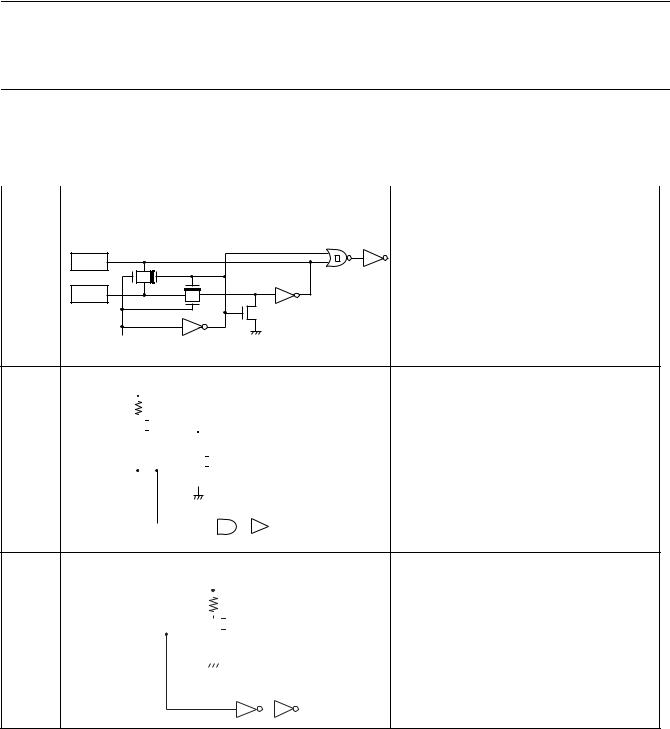
CHAPTER 1 OVERVIEW
1.8I/O Circuit Types
Table 1.8-1 describes the I/O circuit types.
The letters in the circuit column shown in Table 1.8-1 correspond to the letters in the circuit type column shown in Table 1.7-1 .
■ I/O Circuit Types
Table 1.8-1 |
I/O Circuit Types (1/2) |
|
|
|
|
Types |
Circuit |
Remarks |
|
|
|
A |
|
At an oscillation feedback resistance of |
|
|
approximately 500 kΩ |
X1 |
X0 |
Standby control signal
B |
|
|
|
|
|
|
|
|
|
|
|
|
CMOS output |
||
|
|
|
|
|
|
|
|
|
|
|
|
|
|
|
Hysteresis input |
|
|
|
|
|
|
|
|
|
|
|
|
|
|
|
|
|
|
|
|
|
|
|
|
|
P-ch |
|
|
|
|
Pull-up resistor optional |
|
|
|
|
|
|
|
|
|
|
|
|
|
|
|
|
|
|
|
|
|
|
|
|
|
|
|
|
|
|
|
P-ch |
|
|
|
|
|
|
|
|
|
|
|
|
|
|
|
||
|
|
|
|
|
|
|
|
|
|
|
|
|
|
|
|
|
|
|
|
|
|
|
|
|
|
|
|
|
|
|
|
|
|
|
|
|
|
|
|
|
|
|
|
|
|
|
|
N-ch
Input enable


 Port / Resource
C |
|
At an output pull-up resistor (P-ch) of |
||||||||||||||
|
|
|
|
|
|
|
|
P-ch with pull-up, not |
|
approximately 50 kΩ/5.0 V |
||||||
|
|
|
|
|
|
|
|
available for |
|
(not available for MB89F202/F202RA) |
||||||
|
|
|
|
|
|
|
|
|||||||||
|
|
|
|
|
|
|
|
MB89F202/F202RA |
|
N-ch open-drain reset output |
||||||
|
|
|
|
|
|
|
|
|
|
|
|
|
|
|
|
|
|
|
|
|
|
|
|
|
|
|
|
|
|
|
|
|
Hysteresis input |
|
|
|
|
|
|
|
|
|
|
|
|
|
|
|
|
High voltage input tolerable in MB90F202RA |
|
|
|
|
|
|
|
|
|
N-ch |
|||||||
|
|
|
|
|
|
|
|
|
|
Reset |
||||||
|
|
|
|
|
|
|
|
|
|
|
|
|
|
|
|
|
|
|
|
|
|
|
|
|
|
|
|
|
|
|
|
|
|
14
Loading...