


 Loading...
T E C H N I C A L M A N U A L
N S 2 3 2
N S 2 4 2
N S 2 5 2
N S 2 7 2
C O N S T A N T C U R R E N T
P E R I P H E R A L N E R V E S T I M U L A T O R
A N D N E R V E L O C A T O R
Revision I
By I.H
December 2005
Copyright © 2005 Fisher & Paykel Healthcare Ltd
Auckland New Zealand

Page 2 of 40
INTERNATIONAL P O Box 14 348, Panmure, Auckland 6, New Zealand Tel:+64 9 574 0100 Fax:+64 9 574 0158 E-mail:
innervator@fphcare.co.nz Web Site: www.fphcare.com
USA Tel: 1800 446 3908 or +1 949 470 3900 Fax:+1 949 470 3933,
AUSTRALIA Tel:+61 3 9879 5022 Fax:+61 3 9879 5232,
AUSTRIA Tel: 0800 29 31 23 Fax: 0800 29 31 22,
BENELUX Tel: +31 78 644 0924 Fax: +31 78 644 0914,
FRANCE Tel:+33 1 6446 5201 Fax:+33 1 6446 5221,
GERMANY Tel: +49 7182 93777 0 Fax: +49 7182 93777 99,
IRISH REPUBLIC Tel: 1800 409 011,
ITALY Tel:+39 06 7839 2939 Fax:+39 06 7814 7709,
SPAIN Tel:+34 902 013 346 Fax:+34 902 013 379,
UK (EU Authorised Representative) Tel:+44 1628 626 136 Fax:+44 1628 626 146,
Nthn Ireland Tel: 0800 132 189.
Part Number 185 040 670, Revision I, Issued December 2005
Technical Manual for Nerve Stimulator models: NS272, NS242, NS252 (V2.0, V1.0 & 1.1) Technical Manual for Nerve Locator models: NS232 (V2.0)
Note: if the unit is an NS242 with serial number smaller than 031202001629 or an NS252 with serial number smaller than 031202001627, refer to NS252/242 V1.0 & V1.1 Software Technical Manual on page 26
Fisher & Paykel Healthcare have a policy of continued product improvement and reserve the right to alter specifications without notice
Changes made to this technical manual
Wheelie bin symbol added
Maximum voltage in both internal and external mode are better defined
Separate Set Current Offset and Alarm Limits back to the format as per revision G
Include Technical Manual for NS242 and NS252 with V1.0/1.1 Software
NS272/ NS252/ NS242/ NS232 Technical Manual * Revision I* Issued December 2005
|
|
Page 3 of 40 |
|
TABLE OF CONTENTS |
|
INTRODUCTION ............................................................................................................................. |
6 |
|
1 |
GENERAL SPECIFICATIONS – V2.0 ................................................................................ |
8 |
1.1 |
General Product Information (For All Nerve Stim Types) .................................................................. |
8 |
1.2 |
External Mode Electrical Specifications (NS272 & NS252) ............................................................... |
8 |
1.3 |
External Mode Electrical Specifications (NS242 only) ....................................................................... |
9 |
1.4 |
Internal Mode Electrical Specifications (NS272 & NS232) ................................................................ |
9 |
1.5 |
Pulse Types ........................................................................................................................................ |
10 |
2 |
HARDWARE DESCRIPTION - V2.0 ................................................................................ |
11 |
2.1 |
Control (For All Types) ..................................................................................................................... |
11 |
2.2 |
Supply Rails (For All Types) ............................................................................................................. |
11 |
2.3 |
Low Battery Detect (For All Types) .................................................................................................. |
11 |
2.4 |
Beeper (For All Types) ...................................................................................................................... |
12 |
2.5 |
High Voltage Rail (NS272, NS252 & NS242) .................................................................................. |
12 |
2.6 |
Internal Mode Constant Current Controller (NS272 & NS232) ........................................................ |
12 |
2.7 |
Internal Mode Leadset Monitor (NS272 & NS232) .......................................................................... |
12 |
2.8 |
External Mode Constant Current Controller (NS272, NS252 & NS242) .......................................... |
12 |
3 |
TEST POINTS (TP) - V2.0............................................................................................. |
14 |
3.1 |
For All Types ..................................................................................................................................... |
14 |
3.2 |
For NS272, NS252 & NS242............................................................................................................. |
14 |
4 |
SELF TEST - V2.0.......................................................................................................... |
15 |
4.1 |
ROM Test (For All Types)................................................................................................................. |
15 |
4.2 |
Display Test* (For All Types) ........................................................................................................... |
15 |
4.3 |
Model Test (For All Types) ............................................................................................................... |
15 |
4.4 |
Button Test (For All Types)............................................................................................................... |
15 |
4.5 |
Internal Mode Current Test (NS272 & NS232)................................................................................. |
16 |
4.6 |
External Mode Current Test (NS272, NS252 & NS242)................................................................... |
16 |
5 |
ERROR CODES - V2.0 ................................................................................................... |
17 |
6 |
SERVICE INFORMATION (FOR ALL TYPES) - V2.0 ...................................................... |
18 |
7 |
PART LIST - V2.0.......................................................................................................... |
19 |
7.1 |
For All Types ..................................................................................................................................... |
19 |
7.2 |
For NS272, NS252 & NS242............................................................................................................. |
19 |
7.3 |
For NS232 only.................................................................................................................................. |
19 |
8 |
ACCESSORIES - V2.0..................................................................................................... |
20 |
8.1 |
For All Types ..................................................................................................................................... |
20 |
NS272/ NS252/ NS242/ NS232 Technical Manual * Revision I* Issued December 2005
|
|
Page 4 of 40 |
8.2 |
For NS272, NS252 & NS242 ............................................................................................................ |
20 |
8.3 |
For NS272, NS232 ............................................................................................................................ |
20 |
8.4 |
Component Layout Diagram ............................................................................................................. |
21 |
APPENDIX A PRODUCT CHANGE HISTORY (FOR NS272, NS252, NS242) - V2.0............... |
22 |
|
APPENDIX B PRODUCT NUMBERS (FOR ALL TYPES) - V2.0................................................ |
23 |
|
B1. |
Model Number Explanation .............................................................................................................. |
23 |
B2. |
Serial Number Explanation................................................................................................................ |
23 |
B3. |
Product Code Table ........................................................................................................................... |
24 |
NS272/ NS252/ NS242/ NS232 Technical Manual * Revision I* Issued December 2005
|
|
|
Page 5 of 40 |
1 |
GENERAL SPECIFICATIONS – V1.0/V1.1 ..................................................................... |
26 |
|
1.1 |
Electrical Specifications – V1.0/1.1................................................................................................... |
26 |
|
1.2 |
Pulse Types: ROM 999630013 ......................................................................................................... |
26 |
|
1.3 |
Pulse Types: ROM 367020009 ......................................................................................................... |
27 |
|
2 |
HARDWARE DESCRIPTION – V1.0/1.1.......................................................................... |
28 |
|
2.1 |
Control ............................................................................................................................................... |
28 |
|
2.2 |
Reference Rail.................................................................................................................................... |
28 |
|
2.3 |
High Voltage Rail .............................................................................................................................. |
28 |
|
2.4 |
Constant Current Control ................................................................................................................... |
28 |
|
2.5 |
Low Battery Detect ............................................................................................................................ |
28 |
|
2.6 |
Miscellaneous..................................................................................................................................... |
29 |
|
3 |
OPERATIONAL DESCRIPTION – V1.0/1.1 ..................................................................... |
30 |
|
3.1 |
Power Down....................................................................................................................................... |
30 |
|
3.2 |
Self Calibration .................................................................................................................................. |
30 |
|
3.3 |
Pulse Delivery .................................................................................................................................... |
30 |
|
4 |
TEST POINTS – V1.0/1.1............................................................................................... |
31 |
|
5 |
SELF TEST – V1.0/1.1................................................................................................... |
32 |
|
5.1 |
ROM 999630013 ............................................................................................................................... |
32 |
|
5.2 |
ROM 367020009 ............................................................................................................................... |
33 |
|
6 |
SERVICE INFORMATION – V1.0/1.1.............................................................................. |
34 |
|
7 |
PARTS LIST – V1.0/1.1 ................................................................................................. |
35 |
|
8 |
ACCESSORIES – V1.0/1.1.............................................................................................. |
36 |
|
8.1 |
Component Layout Diagram.............................................................................................................. |
36 |
|
APPENDIX A |
SERVICE NOTE – V1.0/1.1................................................................................ |
37 |
|
APPENDIX B |
PRODUCT CHANGE HISTORY – V1.0/1.1 ......................................................... |
38 |
|
APPENDIX C |
PRODUCT NUMBERS – V1.0/1.1........................................................................ |
39 |
|
C1. |
Model Number And Serial Number Explanation............................................................................... |
39 |
|
C2. |
Product Code Table............................................................................................................................ |
40 |
|
NS272/ NS252/ NS242/ NS232 Technical Manual * Revision I* Issued December 2005

Page 6 of 40
INTRODUCTION
Read the operating manual carefully before operating the unit.
Electrostatic sensitive devices
Type BF Equipment (IEC Standard).
 (EU WEEE Standard) Do not throw away. See distributor for appropriate disposal for electrical and electronic components
Caution Dangerous high voltages may exist within this device for up to 1 minute after removal of batteries. The microprocessor may continue to run for up to 10 minutes after removal of batteries. It is recommended that the batteries be removed at least 10 minutes prior to disassembly.
Caution This device contains CMOS and other components which are sensitive to static charges. It is recommended appropriate procedures be followed for disassembly and service.
Caution An explosion is possible if used in the presence of flammable anaesthetics. An explosion may be caused by an arc which could occur if the electrodes come into direct contact as a pulse is being delivered.
Warning In External Mode, this device is to be used with non-invasive electrodes only. If needle electrodes are used in External Mode, localised tissue burning and excessive patient discomfort may result.
NS272/ NS252/ NS242/ NS232 Technical Manual * Revision I* Issued December 2005
T E C H N I C A L M A N U A L
N S 2 3 2
N S 2 4 2
N S 2 5 2
N S 2 7 2
V e r s i o n 2 . 0
C O N S T A N T C U R R E N T
P E R I P H E R A L N E R V E S T I M U L A T O R A N D N E R V E L O C A T O R
NS272/ NS252/ NS242/ NS232 Technical Manual * Revision I* Issued December 2005
NS272/252/242/232 V2.0 Software |
Page 8 of 40 |
1 GENERAL SPECIFICATIONS – V2.0
This part of the manual defines the technical specifications for the NS252 & NS242 Peripheral Nerve Stimulator, NS272 Peripheral Nerve Stimulator & Nerve Locator and NS232 Nerve Locator with version 2.0 software. Refer to the Operating Manual for NS272, NS252, NS242 and NS232 for detailed instructions on how to use the unit.
Any NS242 unit with a serial number smaller than 031202001629 runs on version 1.0 or 1.1 software. Any NS252 unit with a serial number smaller than 031202001627 runs on version 1.0 or 1.1 software. Please refer to the sections from page 26 onwards, for the technical specification.
1.1GENERAL PRODUCT INFORMATION (FOR ALL NERVE STIM TYPES)
Battery Type: 3 times 1.5 V AA type alkaline cells (IEC type LR6)
Battery Life: Up to 160 hours continuous use with alkaline batteries Note: This figure varies greatly depending on choice of External or Internal Mode in NS272, waveforms used and current delivered.
Up to 160 hours continuous use with alkaline batteries in NS232, NS242, NS252
Operating Temperature Range: 0 °C to 35 °C Operating Humidity Range: 0% RH to 65% RH Storage Temperature Range: -25 °C to +40 °C
Storage Humidity Range: 0% RH to 85% RH Dimensions: NS232:
Height = 167 mm, width = 73 mm, depth = 43 mm NS242, NS252 and NS272
Height = 175 mm, width = 73 mm, depth = 43 mm Weight: 255g (185g without batteries)
1.2EXTERNAL MODE ELECTRICAL SPECIFICATIONS (NS272 & NS252)
Output Current Range: |
0 to 160 mA |
Output Current Steps |
5 or 10 mA (programmable) |
Tetanus Frequency |
50 or 100 Hz ± 10% (programmable) |
Output Pulse Type: |
Square, monophasic, constant current, unidirectional |
Output Pulse Width: |
195 ± 5 µs |
Output Pulse Rise Time: |
< 10 µs max (resistive load) |
Output Pulse Fall Time: |
< 10 µs max (resistive load) |
Maximum Internal Voltage: |
420 ± 10% V |
Maximum Output Voltage: |
350 ± 10% V |
Maximum Load Impedance |
For TW, TOF, TET, PTC, DBS |
80 mA |
4 kΩ |
160 mA |
1.8 kΩ |
|
(figures may vary depending on battery condition) |
Set Current Offset: |
|
0 to 80 mA |
± 2.5 mA |
85 to 160mA |
± 5.0 mA |
Alarm Limits: |
± 2.5 mA of the set current |
Default Program: |
10 s twitch |
NS272/ NS252/ NS242/ NS232 Technical Manual * Revision I* Issued December 2005
NS272/252/242/232 V2.0 Software |
Page 9 of 40 |
Default Program Settings: |
|
Tetanus Frequency |
50 Hz |
Maximum Current |
80 mA |
Current Steps |
10 mA |
DBS Pattern |
3.3 |
1.3EXTERNAL MODE ELECTRICAL SPECIFICATIONS (NS242 ONLY)
Output Current Range: |
0 to 80 mA |
Output Pulse Type: |
Square, monophasic, constant current, unidirectional |
Output Pulse Width: |
195 ± 5 µs |
Output Pulse Rise Time: |
< 10 µs max (resistive load) |
Output Pulse Fall Time: |
< 10 µs max (resistive load) |
Maximum Internal Voltage: |
420 ± 10% V |
Maximum Output Voltage: |
350 ± 10% V |
Maximum Load Impedance |
For TW, TOF, TET |
80 mA |
4 kΩ |
|
(figures may vary depending on battery condition) |
Set Current Offset |
|
0 to 80 mA |
± 2.5 mA |
Alarm Limits: |
± 2.5 mA of the set current |
Default Program Settings: |
|
Tetanus Frequency |
50 Hz |
Maximum Current |
80 mA |
Current Steps |
10 mA |
Note: The above specifications can not be guaranteed if the unit is used with a load impedance of more than 5 kΩ.
1.4INTERNAL MODE ELECTRICAL SPECIFICATIONS (NS272 & NS232)
Output Current Range: |
0 to 10 mA |
Output Current Steps: |
0.2 mA between 0.0 and 2.0 mA |
|
0.5 mA between 2.0 and 5.0 mA |
|
1.0 mA between 5.0 and 10.0 mA |
Output Pulse Type: |
Square wave, monophasic, constant current, |
|
unidirectional |
Output Pulse Width: |
195 µs ± 5 µs |
Output Pulse Rise Time: |
< 10 µs max (resistive load) |
Output Pulse Fall Time: |
< 10 µs max (resistive load) |
Maximum Internal Voltage: |
15 V ± 10% |
Maximum Output Voltage: |
10 V ± 10% |
Maximum Load Impedance at 10.0 mA: |
1.0 kΩ |
Set Current Offset: |
|
For 0 - 2.0 mA: |
± 0.15 mA |
For 2.5 - 10.0 mA: |
± 0.3 mA |
Alarm Limits: |
± 0.1 mA of the set current |
Default Program: |
10 s twitch |
NS272/ NS252/ NS242/ NS232 Technical Manual * Revision I* Issued December 2005
NS272/252/242/232 V2.0 Software |
Page 10 of 40 |
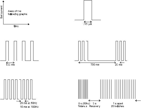
1.5PULSE TYPES
Twitch
±5 µs |
|
|
(All Types) |
Train of four |
Double burst |
±15 ms ±15 ms |
±0.5 ms |
(NS272, NS252, NS242) |
(NS272 & NS252 only) |
Tetanus |
Post tetanic count |
±0.5 ms ±0.2 ms
±0.5 ms |
|
(NS272, NS252) & (NS242 with 20ms at 50Hz |
(NS272 & NS252 only) |
only) |
|
NS272/ NS252/ NS242/ NS232 Technical Manual * Revision I* Issued December 2005
NS272/252/242/232 V2.0 Software |
Page 11 of 40 |
2 HARDWARE DESCRIPTION - V2.0
2.1CONTROL (FOR ALL TYPES)
The core of the system is a masked ROM microprocessor, U6 which has an LCD Driver and 3 Counters/Timers on chip.
The On/Off Button, SW1, works by generating a short pulse at the reset input of U6 via C30.
The remainder of the push-buttons are arranged in a row/column scanning matrix. A diode-OR connection between the rows enables any button to bring the interrupt input of U6 low. The microprocessor is then able to determine exactly which button is being pressed by examining the status of the Port 0 outputs and the Port 2 inputs.
U6 communicates via an I²C bus serial interface to the two A/D and D/A converters, U1 and U3.
The system timing is based on a 10 ms count generated inside U6. This time base is available at TP14.
2.2SUPPLY RAILS (FOR ALL TYPES)
There are four main DC Supply Rails: +VBAT, +VCC, +VREF and +VDD. The first three are derived directly from the battery while the last is under microprocessor control.
+VBAT |
This supply is the raw battery voltage and is used to supply the two switch mode power supplies for |
|
+VDD and the HV Rail. |
+VCC |
This supply is isolated and derived from +VBAT via diode D14 and further smoothed to provide a |
|
more stable voltage for the microprocessor and A/D and D/A converter ICs. |
+VREF |
This supply is maintained at 2.5 V by a three terminal regulator, U4 and is used as the LCD drive |
|
voltage and as the reference voltage for both the A/D and D/A converters. |
+VDD |
This supply, nominally 15 V, is generated by a switch mode converter IC, U5 configured as a boost |
|
mode DC to DC converter. The relevant components are L1, D7 and C29. The switching frequency |
|
is determined by C26. |
|
U5 acts to control the voltage at its VFB input at a level equal to its internal reference voltage of 1.31 |
|
V. Thus the voltage divider R37 and R39 determines the level of +VDD. |
|
The microprocessor is able to turn U5 on by pulling its IC input high via Q20. |
|
+VDD is used to power the CMOS logic and the two current controllers, to drive the two FETs and |
|
supply C4 from which the Internal Mode pulses are generated. |
There is an additional supply of 4 V which is used by the current controllers. This supply is produced by amplifying +VREF and is available at pin 7 of U7.
2.3LOW BATTERY DETECT (FOR ALL TYPES)
The low battery detect works in two stages. Stage one lights up the battery symbol on the LCD as a warning once the battery voltage falls to 3.3 V. Stage two shuts the microcontroller down at 2.9 V, leaving only the battery symbol on the LCD to indicate why the unit is off.
The microcontroller monitors the battery voltage in two different ways. The first is by using A/D channel 3 of U3 and the potential divider R35 and R36. The second way is by monitoring the state of the LBD output of U5. When the IC input of U5 is high, the LBD output of U5 goes low whenever its LBR input falls below its internal reference voltage of 1.31 V nominal.
The microcontroller first checks the state of the LBD output of U5. down and will cease to function further until the batteries are changed. recognise this has occurred.
If it is low then the microcontroller will shut The unit must be turned off and on for U6 to
If the LBD output of U5 is high, the processor will go on to check the voltage at the LBR input of U5 using the A/D converter. If the voltage at the LBR point is too low the battery symbol will appear on the display.
NS272/ NS252/ NS242/ NS232 Technical Manual * Revision I* Issued December 2005
NS272/252/242/232 V2.0 Software |
Page 12 of 40 |
2.4BEEPER (FOR ALL TYPES)
LS1 is a piezoelectric loudspeaker. It is driven with an audio frequency square wave produced by an astable multivibrator, Q17 and Q18. That oscillator is turned on and off by the microcontroller via Q19.
2.5HIGH VOLTAGE RAIL (NS272, NS252 & NS242)
The high voltage rail is an electrolytic capacitor, C11, which is charged up to generate External Mode pulses.
To charge the rail, U6 activates the oscillator U2, by pulling down its reset pin, causing output Q4 to switch at a frequency determined by R15, R16 and C8. Q9 drives the primary of transformer XFORM1. The voltage at the secondary is rectified to charge C11.
When high current pulses are delivered the high voltage rail is regulated to approximately 400 V by comparator U7B. The high voltage rail is monitored by the potential divider R19, R20 and R53 and compared with +VREF. When the voltage at pin 3 of U7 reaches 2.5 V, Q24 is switched on to remove the base drive from Q8 and the oscillator is turned off.
The microcontroller also monitors the voltage across C11 using A/D channel 2 of U3 and the potential divider of R19, R20 and R53. This allows U6 to establish whether the voltage on C11 has reached the lesser of 420 V or (set current x 5000 Ω) and provide some control of the high voltage rail.
2.6INTERNAL MODE CONSTANT CURRENT CONTROLLER (NS272 & NS232)
In order to deliver an Internal Mode constant current pulse, C4 must first be charged up from +VDD through R10. The microcontroller monitors the voltage across C4 via the potential divider R3, R2 and A/D channel 2 of U1.
The microcontroller then sets the level of constant current to be delivered by setting a voltage at the output of the D/A converter of U1.
At the start of the pulse the microcontroller turns Q7 on and Q1 and Q2 off. Under those conditions, the voltage at the collector of Q6 will increase depending on the difference between the voltages at the emitters of Q6 and Q5. The Q6 collector voltage determines how much current the Darlington configuration of Q22 and Q4 conducts. The collector current of Q4 is the current delivered at the output and it develops a proportional voltage across R1. Thus the Q5, Q6 pair maintains the output current equal to the voltage at the output of the D/A converter divided by the resistance of R1.
A/D channel 0 of U1 monitors the voltage across R1. By doing this, U6 is able to determine whether the correct current is being delivered at all times.
Q2 holds Q22 and Q4 in their off-state between pulses and while the unit is switched off, to avoid any output leakage currents.
2.7INTERNAL MODE LEADSET MONITOR (NS272 & NS232)
The microcontroller is able to determine whether the Internal Mode leadset is connected to the unit by monitoring the voltage at A/D channel 3 input of U1.
2.8EXTERNAL MODE CONSTANT CURRENT CONTROLLER (NS272, NS252 & NS242)
An External Mode pulse is generated in a similar way to the Internal Mode pulse.
In order to deliver an External Mode constant current pulse, C11 must first be charged up. The microcontroller monitors the voltage across C11 via the potential divider R19, R20, R53 and A/D channel 2 of U3.
The microcontroller then sets the level of constant current to be delivered by setting a voltage at the output of the D/A converter of U3.
NS272/ NS252/ NS242/ NS232 Technical Manual * Revision I* Issued December 2005
Loading...