Fairchild Semiconductor MMBFJ210, MMBFJ212, MMBFJ211, J211, J212 Datasheet

J210
J211
J212
G |
TO-92 |
|
S D |
MMBFJ210
MMBFJ211
MMBFJ212
G
|
S |
SOT-23 |
D NOTE: Source & Drain |
Mark: 62V / 62W / 62X |
are interchangeable |
N-Channel RF Amplifier
This device is designed for HF/VHF mixer/amplifier and applications where Process 50 is not adequate. Sufficient gain and low noise for sensitive receivers. Sourced from Process 90.
Absolute Maximum Ratings* TA = 25°C unless otherwise noted
Symbol |
Parameter |
Value |
Units |
|
|
|
|
VDG |
Drain-Gate Voltage |
25 |
V |
VGS |
Gate-Source Voltage |
- 25 |
V |
IGF |
Forward Gate Current |
10 |
mA |
TJ ,Tstg |
Operating and Storage Junction Temperature Range |
-55 to +150 |
° C |
*These ratings are limiting values above which the serviceability of any semiconductor device may be impaired.
NOTES:
1)These ratings are based on a maximum junction temperature of 150 degrees C.
2)These are steady state limits. The factory should be consulted on applications involving pulsed or low duty cycle operations.
Thermal Characteristics TA = 25°C unless otherwise noted
Symbol |
Characteristic |
|
Max |
Units |
|
|
|||
|
|
|
|
|
|
|
J210-212 |
*MMBFJ210-212 |
|
PD |
Total Device Dissipation |
350 |
225 |
mW |
|
Derate above 25° C |
2.8 |
1.8 |
mW/° C |
Rθ JC |
Thermal Resistance, Junction to Case |
125 |
|
° C/W |
|
|
|
|
|
Rθ JA |
Thermal Resistance, Junction to Ambient |
357 |
556 |
° C/W |
|
|
|
|
|
*Device mounted on FR-4 PCB 1.6" X 1.6" X 0.06."
MMBFJ212 / 1MMBFJ21 / MMBFJ210 / J212 / 1J21 / J210
1997 Fairchild Semiconductor Corporation |
J210/J211/J212/MMBFJ210/J211/J212, Rev A |

N-Channel RF Amplifier
(continued)
Electrical Characteristics TA = 25°C unless otherwise noted
Symbol |
Parameter |
Test Conditions |
|
Min |
Max |
Units |
|
|
|
|
|
|
|
|
|
OFF CHARACTERISTICS |
|
|
|
|
|
|
|
V ( B R ) G S S |
Gate-Source Breakdown Voltage |
IG = 1.0 μA, V DS = 0 |
|
|
- 25 |
|
V |
IG S S |
Gate Reverse Current |
V G S = 15 V, V D S = 0 |
|
|
|
- 100 |
pA |
V GS(off) |
Gate-Source Cutoff Voltage |
V D S = 15 V, I D = 1.0 nA |
210 |
-1.0 |
-3.0 |
V |
|
|
|
|
|
211 |
- 2.5 |
- 4.5 |
V |
|
|
|
|
212 |
- 4.0 |
- 6.0 |
V |
ON CHARACTERISTICS |
|
|
|
|
|
|
|
|
|
|
|
|
|
|
|
ID S S |
Z e r o - G a t e V o l t a g e D r a i n C u r r e n t * |
V D S = 1 5 V , V G S = 0 |
|
2 1 0 |
2 . 0 |
1 5 |
m A |
|
|
|
|
2 1 1 |
7 . 0 |
2 0 |
m A |
|
|
|
|
2 1 2 |
1 5 |
4 0 |
m A |
SMALL SIGNAL CHARACTERISTICS |
|
|
|
|
|
|
|
|
|
|
|
|
|
|
|
gfs |
Common Source Forward |
VD S = 15 V, V G S = 0, |
f = 1.0 kHz |
|
|
|
|
|
Transconductance |
|
|
210 |
4000 |
12,000 |
μmhos |
|
|
|
|
211 |
6000 |
12,000 |
μmhos |
|
|
|
|
212 |
7000 |
12,000 |
μmhos |
go s s |
Common Source Output |
VD S = 15 V, V G S = 0, |
f = 1.0 kHz |
|
200 |
μmhos |
|
|
Conductance |
|
|
|
|
|
|
*Pulse Test: Pulse Width ≤ 300 μS |
|
|
|
|
|
|
|
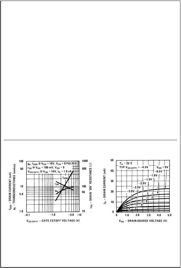
Typical Characteristics
Parameter Interactions |
Common Drain-Source |
MMBFJ212 / MMBFJ211 / MMBFJ210 / J212 / J211 / J210
 Loading...