


Fairchild Semiconductor ILC5061M46, ILC5061M31, ILC5061M29, ILC5061M28, ILC5061AM25 Datasheet
...
www.fairchildsemi.com
ILC5061
Power Supply reset Monitor with 1% Precision
Features
•All-CMOS design in SOT-23 or SC70 package
•±1% precision in Reset Detection
•Only 1µA of Iq
•2mA of sink current capability
•Built-in hysteresis of 5% of detection voltage
•Voltage options of 2.6, 2.9, 3.1, 4.4, and 4.6V fit most supervisory applications
•Open-Drain Reset Output
Applications
•Microprocessor reset circuits
•Memory battery back-up circuitry
•Power-on reset circuits
•Portable and battery powered electronics
Description
All-CMOS Monitor circuits in either a 3-lead SOT-23 or SC70 package offer the best performance in power consumption and accuracy.
The ILC5061 comes in a series of ±1% accurate trip voltages to fit most microprocessor applications. Even though its output can sink 2mA, the device draws only 1µA in normal operation.
Additionally, a built-in hysteresis of 5% of detect voltage simplifies system design.
Block Diagram |
|
|
Pin Package Configurations |
||
VIN |
|
|
|
Top View |
|
VOUT |
VOUT |
1 |
|
VOUT |
1 |
|
|
|
SC-70 |
3 VIN |
SOT-23 3 VIN |
VREF |
VSS |
2 |
|
VSS |
2 |
|
|
||||
VSS |
|
|
|
|
|
Rev. 2.5 1/2/03

ILC5061 PRODUCT SPECIFICATION
Absolute Maximum Ratings
Parameter |
|
Symbol |
Ratings |
Units |
|
|
|
|
|
Input Voltages |
|
VIN |
12 |
V |
Output Current |
|
IOUT |
50 |
mA |
Output Voltages |
|
VOUT |
VSS-0.3~+VIN+03 |
V |
Continuous Total |
SOT 23 |
Pd |
150 |
mW |
Power Dissipation |
|
|
|
|
|
|
|
|
|
Operation Ambient temperature |
|
T |
-30~+80 |
oC |
|
|
opr |
|
|
Storage Temperature |
|
T |
-40~+125 |
oC |
|
|
stg |
|
|
Electrical Characteristics TA = 25°C
Parameter |
Symbol |
Conditions |
Min |
Type |
Max |
Units |
|
|
|
|
|
|
|
Detect Fail Voltage |
VDF |
|
VDF X 0.99 |
VDF |
VDF X 1.01 |
V |
Hysteresis Range |
VHYS |
|
VDF X 0.02 |
VDF X 0.05 |
VDF X 0.08 |
V |
|
|
VIN = 1.5V |
|
0.9 |
2.6 |
|
Supply Current |
ISS |
VIN = 2.0V |
|
1.0 |
3.0 |
|
VIN = 3.0V |
|
1.3 |
3.4 |
µA |
||
|
|
VIN = 4.0V |
|
1.6 |
3.8 |
|
|
|
|
2.0 |
4.2 |
|
|
|
|
VIN = 5.0V |
|
|
||
|
|
|
|
|
|
|
Operating Voltage |
VIN |
VDF = 2.1~ 6.0V |
1.5 |
|
10.0 |
V |
|
|
N-ch VDS = 0.5V |
|
|
|
|
Output Current |
IOUT |
VIN = 1.0V |
|
2.2 |
|
|
VIN = 2.0V |
|
7.7 |
|
mA |
||
|
|
VIN = 3.0V |
|
10.1 |
|
|
|
|
|
11.5 |
|
|
|
|
|
VIN = 4.0V |
|
|
|
|
|
|
|
13.0 |
|
|
|
|
|
VIN = 5.0V |
|
|
|
|
Temperature Charac- |
DVDF/(DTopr * VDF) |
-30oC<Topr<80oC |
-200 |
+100 |
+200 |
Ppm/ oC |
teristics |
|
|
|
|
|
|
Delay Time Release |
TDLY |
|
|
|
|
|
Voltage Output Inver- |
(VDR to VOUT |
|
|
|
0.1 |
ms |
sion) |
inversion) |
|
|
|
|
|
|
|
|
|
|
|
|
|
|
|
|
|
|
|
Note: |
|
|
|
|
|
|
1. An additional resistor between the VIN pin and supply voltage may cause deterioration of the characteristics due to increasing VDR.
2 |
Rev. 2.5 1/2/03 |
PRODUCT SPECIFICATION |
ILC5061 |
|
|
Functional Description
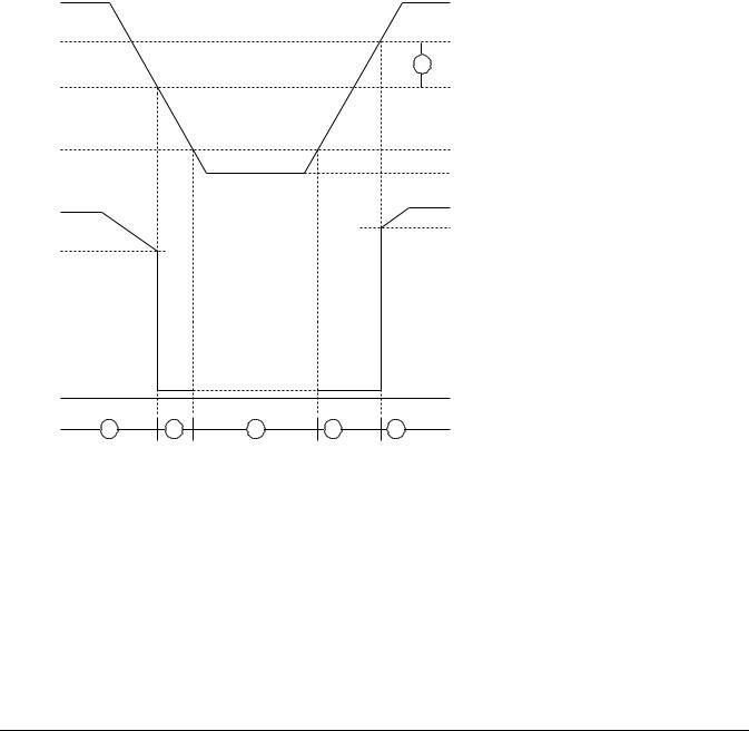
The following designators 1~6 refer to the timing diagram below.
1.While the input voltage (VIN) is higher than the detect voltage (VDF), the VOUT output pin is at high impedance state.
2.When the input VIN voltage falls lower than VDF, VOUT drops near to ground voltage
3.If the input voltage further decreases below the minimum operating voltage (VMIN), the VOUT output becomes unstable. In this condition, if the VOUT pin is pulled up, VOUT indicates the VIN voltage.
4.During an increase of the input voltage from the VSS voltage, VOUT is not stable in the voltage below the VMIN. Exceeding that level, the output stays at the ground level (VSS) between the minimum operating voltage (VMIN) and the detect release voltage (VDR).
5.If the input voltage increases more than VDR, then the VOUT output pin is at high impedance state.
6.The difference between VDR and VDF is the hysteresis in the system.
INPUT VOLTAGE (VIN)
DETECT RELEASE VOLTAGE (VDR)
6
DETECT FAIL VOLTAGE (VDF)
MINIMUM OPERATING VOLTAGE (VMIN)
GROUND VOLTAGE (VSS)
OUTPUT VOLTAGE (VOUT)
GROUND VOLTAGE (VSS)
1 |
2 |
3 |
4 |
5 |
Rev. 2.5 1/2/03 |
3 |
 Loading...