


September 1986
Revised February 2000
DM7400
Quad 2-Input NAND Gates
General Description
This device contains four independent gates each of which performs the logic NAND function.
Ordering Code:
Order Number |
Package Number |
Package Description |
|
|
|
DM7400M |
M14A |
14-Lead Small Outline Integrated Circuit (SOIC), JEDEC MS-012, 0.150 Narrow |
|
|
|
DM7400N |
N14A |
14-Lead Plastic Dual-In-Line Package (PDIP), JEDEC MS-001, 0.300 Wide |
|
|
|
Devices also available in Tape and Reel. Specify by appending the suffix letter “X” to the ordering code.
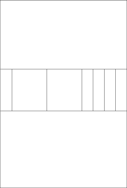
Connection Diagram |
Function Table |
|
|
|
|
||
|
|
|
|
Y = |
AB |
|
|
|
|
|
|
|
|
|
|
|
|
Inputs |
|
|
|
Output |
|
|
|
|
|
|
|
||
|
|
A |
|
B |
|
Y |
|
|
|
|
|
|
|
|
|
|
|
L |
|
L |
|
H |
|
|
|
L |
|
H |
|
H |
|
|
|
H |
|
L |
|
H |
|
|
|
H |
|
H |
|
L |
|
|
|
|
|
|
|
|
|
|
H = HIGH Logic Level |
|
|
|
|
||
|
L = LOW Logic Level |
|
|
|
|
||
Gates NAND Input-2 Quad DM7400
© 2000 Fairchild Semiconductor Corporation |
DS006613 |
www.fairchildsemi.com |
DM7400
Absolute Maximum Ratings(Note 1)
Supply Voltage |
7V |
Note 1: The “Absolute Maximum Ratings” are those values beyond which |
|
the safety of the device cannot be guaranteed. The device should not be |
|||
Input Voltage |
5.5V |
operated at these limits. The parametric values defined in the Electrical |
|
Characteristics tables are not guaranteed at the absolute maximum ratings. |
|||
Operating Free Air Temperature Range |
0°C to +70°C |
||
The “Recommended Operating Conditions” table will define the conditions |
|||
Storage Temperature Range |
−65°C to +150°C |
for actual device operation. |
|
|
Recommended Operating Conditions
Symbol |
Parameter |
Min |
Nom |
Max |
Units |
|
|
|
|
|
|
VCC |
Supply Voltage |
4.75 |
5 |
5.25 |
V |
VIH |
HIGH Level Input Voltage |
2 |
|
|
V |
VIL |
LOW Level Input Voltage |
|
|
0.8 |
V |
IOH |
HIGH Level Output Current |
|
|
−0.4 |
mA |
IOL |
LOW Level Output Current |
|
|
16 |
mA |
TA |
Free Air Operating Temperature |
0 |
|
70 |
°C |
Electrical Characteristics
over recommended operating free air temperature range (unless otherwise noted)
Symbol |
Parameter |
Conditions |
Min |
Typ |
Max |
Units |
|
(Note 2) |
|||||||
|
|
|
|
|
|
||
|
|
|
|
|
|
|
|
VI |
Input Clamp Voltage |
VCC = Min, II = −12 mA |
|
|
−1.5 |
V |
|
VOH |
HIGH Level Output |
VCC = Min, IOH = Max |
2.4 |
3.4 |
|
V |
|
|
Voltage |
VIL = Max |
|
||||
|
|
|
|
|
|||
VOL |
LOW Level Output |
VCC = Min, IOL = Max |
|
0.2 |
0.4 |
V |
|
|
Voltage |
VIH = Min |
|
||||
|
|
|
|
|
|||
II |
Input Current @ Max Input Voltage |
VCC = Max, VI = 5.5V |
|
|
1 |
mA |
|
IIH |
HIGH Level Input Current |
VCC = Max, VI = 2.4V |
|
|
40 |
μA |
|
IIL |
LOW Level Input Current |
VCC = Max, VI = 0.4V |
|
|
−1.6 |
mA |
|
IOS |
Short Circuit Output Current |
VCC = Max (Note 3) |
−18 |
|
−55 |
mA |
|
ICCH |
Supply Current with Outputs HIGH |
VCC = Max |
|
4 |
8 |
mA |
|
ICCL |
Supply Current with Outputs LOW |
VCC = Max |
|
12 |
22 |
mA |
Note 2: All typicals are at VCC = 5V, TA = 25°C.
Note 3: Not more than one output should be shorted at a time.
Switching Characteristics
at VCC = 5V and TA = 25°C
Symbol |
Parameter |
Conditions |
Min |
Max |
Units |
|
|
|
|
|
|
tPLH |
Propagation Delay Time |
CL = 15 pF |
|
22 |
ns |
|
LOW-to-HIGH Level Output |
RL = 400Ω |
|
||
|
|
|
|
||
tPHL |
Propagation Delay Time |
|
|
15 |
ns |
|
HIGH-to-LOW Level Output |
|
|
||
|
|
|
|
|
|
|
|
|
|
|
|
www.fairchildsemi.com |
2 |
 Loading...