Fairchild Semiconductor CD4007CN, CD4007CMX, CD4007CM Datasheet

October 1987
Revised January 1999
CD4007C
Dual Complementary Pair Plus Inverter
General Description
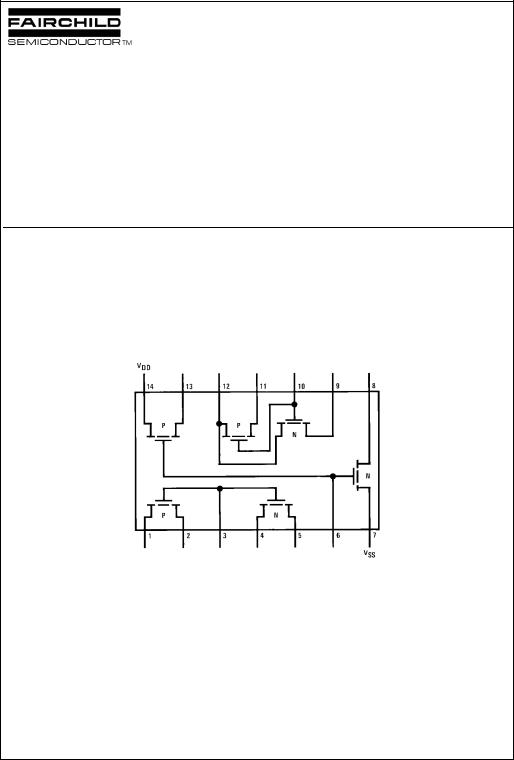
The CD4007C consists of three complementary pairs of N- and P-channel enhancement mode MOS transistors suitable for series/shunt applications. All inputs are protected from static discharge by diode clamps to VDD and VSS.
For proper operation the voltages at all pins must be constrained to be between VSS − 0.3V and VDD + 0.3V at all times.
Features
■Wide supply voltage range: 3.0V to 15V
■High noise immunity: 0.45 VCC (typ.)
Ordering Code:
Order Number |
Package Number |
Package Description |
|
|
|
CD4007CM |
M14A |
14-Lead Small Outline Integrated Circuit (SOIC), JEDEC MS-120, 0.150” Narrow |
|
|
|
CD4007CN |
N14A |
14-Lead Plastic Dual-In-Line Package (PDIP), JEDEC MS–001, 0.300” Wide |
|
|
|
Devices also available in Tape and Reel. Specify by appending the suffix letter “X” to the ordering code.
Connection Diagram
Pin Assignments for DIP and SOIC
Note: All P-channel substrates are connected to VDD and all N-channel substrates are connected to VSS.
Top View
Inverter Plus Pair Complementary Dual CD4007C
© 1999 Fairchild Semiconductor Corporation |
DS005943.prf |
www.fairchildsemi.com |

CD4007C
Absolute Maximum Ratings(Note 1)
Voltage at Any Pin |
VSS −0.3V to VDD +0.3V |
Operating Temperature Range |
−40°C to +85°C |
Storage Temperature Range |
−65°C to +150°C |
Power Dissipation (PD) |
|
Dual-In-Line |
700 mW |
Small Outline |
500 mW |
Operating VDD Range |
VSS +3.0V to VSS +15V |
Lead Temperature |
|
(Soldering, 10 seconds) |
260°C |
Note 1: This device should not be connected to circuits with the power on because high transient voltages may cause permanent damage.
DC Electrical Characteristics
|
|
|
|
|
|
|
|
Limits |
|
|
|
|
|
|
|
|
|
|
|
|
|
|
|
|
|
||
Symbol |
Parameter |
Conditions |
|
−40°C |
|
+25°C |
|
|
+85°C |
Units |
|||
|
|
|
|
Min |
Typ |
Max |
Min |
Typ |
Max |
Min |
Typ |
Max |
|
|
|
|
|
|
|
|
|
|
|
|
|
|
|
IL |
Quiescent Device |
VDD = 5.0V |
|
|
0.5 |
|
0.005 |
0.05 |
|
|
15 |
μA |
|
|
Current |
VDD = 10V |
|
|
1.0 |
|
0.005 |
1.0 |
|
|
30 |
μA |
|
PD |
Quiescent Device |
VDD = 5.0V |
|
|
2.5 |
|
0.025 |
2.5 |
|
|
75 |
μW |
|
|
Dissipation Package |
VDD = 10V |
|
|
10 |
|
0.05 |
10 |
|
|
300 |
μW |
|
VOL |
Output Voltage |
VDD = 5.0V |
|
|
0.05 |
|
0 |
0.01 |
|
|
0.05 |
V |
|
|
LOW Level |
VDD = 10V |
|
|
0.05 |
|
0 |
0.01 |
|
|
0.05 |
V |
|
VOH |
Output Voltage |
VDD = 5.0V |
4.95 |
|
|
4.95 |
5.0 |
|
4.95 |
|
|
V |
|
|
HIGH Level |
VDD = 10V |
9.95 |
|
|
9.95 |
10 |
|
9.95 |
|
|
V |
|
VNL |
Noise Immunity |
VDD = 5.0V, VO = 3.6V |
|
|
1.5 |
|
2.25 |
1.5 |
|
|
1.4 |
V |
|
|
(All inputs) |
VDD = 10V, VO = 7.2V |
|
|
3.0 |
|
4.5 |
3.0 |
|
|
2.9 |
V |
|
VNH |
Noise Immunity |
VDD = 5.0V, VO = 0.95V |
3.6 |
|
|
3.5 |
2.25 |
|
3.5 |
|
|
V |
|
|
(All Inputs) |
VDD = 10V, VO = 2.9V |
7.1 |
|
|
7.0 |
4.5 |
|
7.0 |
|
|
V |
|
IDN |
Output Drive Current |
VDD = 5.0V, VO = 0.4V, VI = VDD |
0.35 |
|
|
0.3 |
1.0 |
|
0.24 |
|
|
mA |
|
|
N-Channel |
VDD = 10V, VO = 0.5V, VI = VDD |
1.2 |
|
|
1.0 |
2.5 |
|
0.8 |
|
|
mA |
|
IDP |
Output Drive Current |
VDD = 5.0V, VO = 2.5V, VI = VSS |
−1.3 |
|
|
−1.1 |
−4.0 |
|
−0.9 |
|
|
mA |
|
|
P-Channel |
VDD = 10V, VO = 9.5V, VI = VSS |
−0.65 |
|
|
−0.55 |
−2.5 |
|
−0.45 |
|
|
mA |
|
II |
Input Current |
|
|
|
|
|
|
10 |
|
|
|
|
pA |
AC Electrical Characteristics (Note 2)
TA = 25°C and CL = 15 pF and rise and fall times = 20 ns. Typical temperature coefficient for all values of VDD = 0.3%/°C
Symbol |
Parameter |
Conditions |
Min |
Typ |
Max |
Units |
|
|
|
|
|
|
|
tPLH = tPHL |
Propagation Delay Time |
VDD = 5.0V |
|
35 |
75 |
ns |
|
|
VDD = 10V |
|
20 |
50 |
ns |
tTLH = tTHL |
Transition Time |
VDD = 5.0V |
|
50 |
100 |
ns |
|
|
VDD = 10V |
|
30 |
50 |
ns |
CI |
Input Capacitance |
Any Input |
|
5 |
|
pF |
Note 2: AC Parameters are guaranteed by DC correlated testing.
www.fairchildsemi.com |
2 |
 Loading...