Fairchild PN4117, PN4118, PN4119, MMBF4117, MMBF4118 service manual
...
|
|
|
|
|
|
|
|
|
MMBF4117 |
|
|
|
|
|
|
|
|
|
|
|
|
|
|
|
|
|
|
|
|
|
|
|
|
|
|
|
|
|
|
|
|
|
|
|
|
|
PN4117 |
||
|
|
|
|
|
|
|
PN4118 |
MMBF4118 |
|
|
|
|
|
|
|
|
PN4119 |
MMBF4119 |
|
|
G |
|
|
|
S |
G |
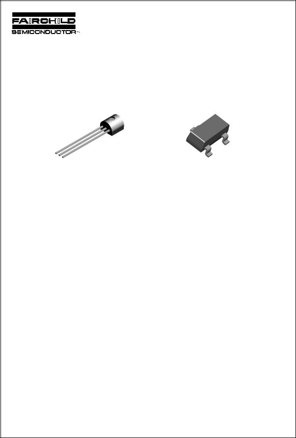
TO-92 |
|
S D |
SOT-23 |
D |
Mark: 61A / 61C / 61E
NOTE: Source & Drain
are interchangeable
N-Channel Switch
This device is designed for low current DC and audio applications. These devices provide excellent performance as input stages for sub-picoamp instrumentation or any high impedance signal sources. Sourced from Process 53.
Absolute Maximum Ratings* TA = 25°C unless otherwise noted
Symbol |
Parameter |
Value |
Units |
|
|
|
|
VDG |
Drain-Gate Voltage |
40 |
V |
VGS |
Gate-Source Voltage |
- 40 |
V |
IGF |
Forward Gate Current |
50 |
mA |
TJ ,Tstg |
Operating and Storage Junction Temperature Range |
-55 to +150 |
° C |
|
|
|
|
*These ratings are limiting values above which the serviceability of any semiconductor device may be impaired.
NOTES:
1)These ratings are based on a maximum junction temperature of 150 degrees C.
2)These are steady state limits. The factory should be consulted on applications involving pulsed or low duty cycle operations.
Thermal Characteristics TA = 25°C unless otherwise noted
Symbol |
Characteristic |
|
Max |
Units |
|
|
|
|
|
|
|
|
|
PN4117-4119 |
|
*MMBF4117-4119 |
|
PD |
Total Device Dissipation |
350 |
|
225 |
mW |
|
Derate above 25° C |
2.8 |
|
1.8 |
mW/° C |
Rθ JC |
Thermal Resistance, Junction to Case |
125 |
|
|
° C/W |
|
|
|
|
|
|
Rθ JA |
Thermal Resistance, Junction to Ambient |
357 |
|
556 |
° C/W |
*Device mounted on FR-4 PCB 1.6" X 1.6" X 0.06."
4119 / 4118 / MMBF4117 / 4119 / 4118 / PN4117
1997 Fairchild Semiconductor Corporation

N-Channel Switch
(continued)
Electrical Characteristics TA = 25°C unless otherwise noted
Symbol |
Parameter |
Test Conditions |
|
Min |
Max |
Units |
|
|
|
|
|
|
|
|
|
OFF CHARACTERISTICS |
|
|
|
|
|
|
|
V(BR)GSS |
Gate-Source Breakdown Voltage |
IG = - 1.0 A, VDS = 0 |
|
- 40 |
|
V |
|
|
|
|
|
|
|
|
|
IGSS |
Gate Reverse Current |
VGS = - 20 V, VDS = 0 |
|
|
- 10 |
pA |
|
|
|
VGS = - 20 V, VDS = 0, TA = 150° C |
|
- 25 |
nA |
||
VGS(off) |
Gate-Source Cutoff Voltage |
VDS = - 10 V, ID = 1.0 nA |
4117 |
- 0.6 |
- 1.8 |
V |
|
|
|
|
4118 |
- 1.0 |
- 3.0 |
V |
|
|
|
|
4119 |
- 2.0 |
- 6.0 |
V |
|
ON CHARACTERISTICS |
|
|
|
|
|
|
|
IDSS |
Zero-Gate Voltage Drain Current* |
VDS = 10 V, VGS = 0 |
4117 |
30 |
90 |
A |
|
|
|
|
4118 |
80 |
240 |
A |
|
|
|
|
4119 |
200 |
600 |
A |
|
SMALL-SIGNAL CHARACTERISTICS |
|
|
|
|
|
|
|
|
|
|
|
|
|
|
|
gfs |
Common-Source Forward |
VDS = 10 V VGS = 0, f= 1.0 kHz |
70 |
210 |
|
|
|
|
Transconductance |
|
4117 |
mhos |
|||
|
|
|
4118 |
80 |
250 |
mhos |
|
|
|
|
4119 |
100 |
330 |
mhos |
|
goss |
Common-Source Output |
VDS = 10 V VGS = 0, f= 1.0 kHz |
|
3.0 |
|
|
|
|
Conductance |
|
4117 |
|
mhos |
||
|
|
|
4118 |
|
5.0 |
mhos |
|
|
|
|
4119 |
|
10 |
mhos |
|
Re(yfs) |
Common-Source Forwad |
VDS = 10 V, VGS = 0, f= 30 MHz |
60 |
|
|
|
|
|
Transconductance |
|
4117 |
|
mhos |
||
|
|
|
4118 |
70 |
|
mhos |
|
|
|
|
4119 |
90 |
|
mhos |
|
Ciss |
Input Capacitance |
VDS = 10 V, VGS = 0, f= 1.0 kHz |
|
3.0 |
pF |
|
|
Crss |
Reverse Transfer Capacitance |
VDS = 10 V, VGS = 0, f= 1.0 MHz, |
|
1.5 |
pF |
|
|
*Pulse Test: Pulse Width ≤ 300 s, Duty Cycle ≤ 1.0%
4119 / 4118 / MMBF4117 / 4119 / 4118 / PN4117
 Loading...