


MVME3100
Table of contents
 Loading...
MVME3100 Single Board Computer
Installation and Use
P/N: 6806800M28C
December 2012
Embedded Computing for
Business-Critical Continuity
TM

©
2011 Emerson
All rights reserved.
Trademarks
Emerson, Business-Critical Continuity, Emerson Network Power and the Emerson Network Power logo are trademarks and service
marks of Emerson Electric Co.
owners.
®
Intel
is a trademark or registered trademark of Intel Corporation or its subsidiaries in the United States and other countries.
™
and all other Java-based marks are trademarks or registered trademarks of Sun Microsystems, Inc. in the U.S. and other
Java
countries.
Microsoft
Microsoft Corporation.
PICMG
Industrial Computer Manufacturers Group.
UNIX
®
, Windows® and Windows Me® are registered trademarks of Microsoft Corporation; and Windows XP™ is a trademark of
®
, CompactPCI®, AdvancedTCA™ and the PICMG, CompactPCI and AdvancedTCA logos are registered trademarks of the PCI
®
is a registered trademark of The Open Group in the United States and other countries.
©
2008 Emerson Electric Co. All other product or service names are the property of their respective
Notice
While reasonable efforts have been made to assure the accuracy of this document, Emerson assumes no liability resulting from any
omissions in this document, or from the use of the information obtained therein. Emerson reserves the right to revise this document
and to make changes from time to time in the content hereof without obligation of Emerson to notify any person of such revision or
changes.
Electronic versions of this material may be read online, downloaded for personal use, or referenced in another document as a URL to
a Emerson website. The text itself may not be published commercially in print or electronic form, edited, translated, or otherwise
altered without the permission of Emerson,
It is possible that this publication may contain reference to or information about Emerson products (machines and programs),
programming, or services that are not available in your country. Such references or information must not be construed to mean that
Emerson intends to announce such Emerson products, programming, or services in your country.
Limited and Restricted Rights Legend
If the documentation contained herein is supplied, directly or indirectly, to the U.S. Government, the following notice shall apply
unless otherwise agreed to in writing by Emerson.
Use, duplication, or disclosure by the Government is subject to restrictions as set forth in subparagraph (b)(3) of the Rights in
Technical Data clause at DFARS 252.227-7013 (Nov. 1995) and of the Rights in Noncommercial Computer Software and
Documentation clause at DFARS 252.227-7014 (Jun. 1995).
Contact Address
Emerson Network Power - Embedded Computing
2900 South Diablo Way, Suite 190
Tempe, AZ 85282
USA

Contents
Contents
About this Manual . . . . . . . . . . . . . . . . . . . . . . . . . . . . . . . . . . . . . . . . . . . . . . . . . . . . . . . . . . . . . . . . . . . . . . . 13
1 Hardware Preparation and Installation . . . . . . . . . . . . . . . . . . . . . . . . . . . . . . . . . . . . . . . . . . . . . . . . . 19
1.1 Overview . . . . . . . . . . . . . . . . . . . . . . . . . . . . . . . . . . . . . . . . . . . . . . . . . . . . . . . . . . . . . . . . . . . . . . . . . . 19
1.2 Getting Started . . . . . . . . . . . . . . . . . . . . . . . . . . . . . . . . . . . . . . . . . . . . . . . . . . . . . . . . . . . . . . . . . . . . 19
1.2.1 Overview of Startup Procedures. . . . . . . . . . . . . . . . . . . . . . . . . . . . . . . . . . . . . . . . . . . . . . . . 19
1.2.2 Unpacking Guidelines . . . . . . . . . . . . . . . . . . . . . . . . . . . . . . . . . . . . . . . . . . . . . . . . . . . . . . . . 20
1.3 Configuring Hardware . . . . . . . . . . . . . . . . . . . . . . . . . . . . . . . . . . . . . . . . . . . . . . . . . . . . . . . . . . . . . . 20
1.3.1 MVME3100 Layout . . . . . . . . . . . . . . . . . . . . . . . . . . . . . . . . . . . . . . . . . . . . . . . . . . . . . . . . . . . 21
1.3.2 Configuration Switch (S4) . . . . . . . . . . . . . . . . . . . . . . . . . . . . . . . . . . . . . . . . . . . . . . . . . . . . . 24
1.3.3 Geographical Address Switch (S3). . . . . . . . . . . . . . . . . . . . . . . . . . . . . . . . . . . . . . . . . . . . . . 25
1.3.4 PMC I/O Voltage Configuration . . . . . . . . . . . . . . . . . . . . . . . . . . . . . . . . . . . . . . . . . . . . . . . . 27
1.3.5 RTM SEEPROM Address Switch (S1). . . . . . . . . . . . . . . . . . . . . . . . . . . . . . . . . . . . . . . . . . . . . 27
1.4 Installing Hardware . . . . . . . . . . . . . . . . . . . . . . . . . . . . . . . . . . . . . . . . . . . . . . . . . . . . . . . . . . . . . . . . . 28
1.5 Connecting to Peripherals . . . . . . . . . . . . . . . . . . . . . . . . . . . . . . . . . . . . . . . . . . . . . . . . . . . . . . . . . . . 29
1.6 Completing the Installation . . . . . . . . . . . . . . . . . . . . . . . . . . . . . . . . . . . . . . . . . . . . . . . . . . . . . . . . . . 31
2 Startup and Operation . . . . . . . . . . . . . . . . . . . . . . . . . . . . . . . . . . . . . . . . . . . . . . . . . . . . . . . . . . . . . . . . 33
2.1 Introduction . . . . . . . . . . . . . . . . . . . . . . . . . . . . . . . . . . . . . . . . . . . . . . . . . . . . . . . . . . . . . . . . . . . . . . . 33
2.2 Applying Power . . . . . . . . . . . . . . . . . . . . . . . . . . . . . . . . . . . . . . . . . . . . . . . . . . . . . . . . . . . . . . . . . . . . 33
2.3 Switches and Indicators . . . . . . . . . . . . . . . . . . . . . . . . . . . . . . . . . . . . . . . . . . . . . . . . . . . . . . . . . . . . . 33
3 MOTLoad Firmware . . . . . . . . . . . . . . . . . . . . . . . . . . . . . . . . . . . . . . . . . . . . . . . . . . . . . . . . . . . . . . . . . . 39
3.1 Overview . . . . . . . . . . . . . . . . . . . . . . . . . . . . . . . . . . . . . . . . . . . . . . . . . . . . . . . . . . . . . . . . . . . . . . . . . . 39
3.2 Implementation and Memory Requirements . . . . . . . . . . . . . . . . . . . . . . . . . . . . . . . . . . . . . . . . . . . 39
3.3 MOTLoad Commands . . . . . . . . . . . . . . . . . . . . . . . . . . . . . . . . . . . . . . . . . . . . . . . . . . . . . . . . . . . . . . . 39
3.3.1 Utilities . . . . . . . . . . . . . . . . . . . . . . . . . . . . . . . . . . . . . . . . . . . . . . . . . . . . . . . . . . . . . . . . . . . . . 39
3.3.2 Tests . . . . . . . . . . . . . . . . . . . . . . . . . . . . . . . . . . . . . . . . . . . . . . . . . . . . . . . . . . . . . . . . . . . . . . . 40
3.3.3 Command List . . . . . . . . . . . . . . . . . . . . . . . . . . . . . . . . . . . . . . . . . . . . . . . . . . . . . . . . . . . . . . . 41
3.4 Using the Command Line Interface . . . . . . . . . . . . . . . . . . . . . . . . . . . . . . . . . . . . . . . . . . . . . . . . . . . 46
3.4.1 Command Line Rules . . . . . . . . . . . . . . . . . . . . . . . . . . . . . . . . . . . . . . . . . . . . . . . . . . . . . . . . . 48
3.4.2 Command Line Help. . . . . . . . . . . . . . . . . . . . . . . . . . . . . . . . . . . . . . . . . . . . . . . . . . . . . . . . . . 48
3.5 Firmware Settings . . . . . . . . . . . . . . . . . . . . . . . . . . . . . . . . . . . . . . . . . . . . . . . . . . . . . . . . . . . . . . . . . . 49
3.5.1 Default VME Settings . . . . . . . . . . . . . . . . . . . . . . . . . . . . . . . . . . . . . . . . . . . . . . . . . . . . . . . . . 49
MVME3100 Single Board Computer Installation and Use (6806800M28C)
3

Contents
Contents
Contents
3.5.2 Control Register/Control Status Register Settings . . . . . . . . . . . . . . . . . . . . . . . . . . . . . . . . 53
3.5.3 Displaying VME Settings . . . . . . . . . . . . . . . . . . . . . . . . . . . . . . . . . . . . . . . . . . . . . . . . . . . . . . 53
3.5.4 Editing VME Settings . . . . . . . . . . . . . . . . . . . . . . . . . . . . . . . . . . . . . . . . . . . . . . . . . . . . . . . . . 54
3.5.5 Deleting VME Settings . . . . . . . . . . . . . . . . . . . . . . . . . . . . . . . . . . . . . . . . . . . . . . . . . . . . . . . . 55
3.5.6 Restoring Default VME Settings . . . . . . . . . . . . . . . . . . . . . . . . . . . . . . . . . . . . . . . . . . . . . . . . 55
3.6 Remote Start . . . . . . . . . . . . . . . . . . . . . . . . . . . . . . . . . . . . . . . . . . . . . . . . . . . . . . . . . . . . . . . . . . . . . . 56
3.7 Alternate Boot Images and Safe Start . . . . . . . . . . . . . . . . . . . . . . . . . . . . . . . . . . . . . . . . . . . . . . . . . 57
3.8 Firmware Startup Sequence Following Reset . . . . . . . . . . . . . . . . . . . . . . . . . . . . . . . . . . . . . . . . . . . 57
3.9 Firmware Scan for Boot Image . . . . . . . . . . . . . . . . . . . . . . . . . . . . . . . . . . . . . . . . . . . . . . . . . . . . . . . 58
3.10 Boot Images . . . . . . . . . . . . . . . . . . . . . . . . . . . . . . . . . . . . . . . . . . . . . . . . . . . . . . . . . . . . . . . . . . . . . . . 60
3.10.1 Checksum Algorithm . . . . . . . . . . . . . . . . . . . . . . . . . . . . . . . . . . . . . . . . . . . . . . . . . . . . . . . . . 60
3.10.2 Image Flags . . . . . . . . . . . . . . . . . . . . . . . . . . . . . . . . . . . . . . . . . . . . . . . . . . . . . . . . . . . . . . . . . 61
3.10.3 User Images . . . . . . . . . . . . . . . . . . . . . . . . . . . . . . . . . . . . . . . . . . . . . . . . . . . . . . . . . . . . . . . . . 62
3.10.4 Alternate Boot Data Structure . . . . . . . . . . . . . . . . . . . . . . . . . . . . . . . . . . . . . . . . . . . . . . . . . 63
3.10.5 Alternate Boot Images and Safe Start . . . . . . . . . . . . . . . . . . . . . . . . . . . . . . . . . . . . . . . . . . . 63
3.10.6 Boot Image Firmware Scan . . . . . . . . . . . . . . . . . . . . . . . . . . . . . . . . . . . . . . . . . . . . . . . . . . . . 64
3.11 Startup Sequence . . . . . . . . . . . . . . . . . . . . . . . . . . . . . . . . . . . . . . . . . . . . . . . . . . . . . . . . . . . . . . . . . . 65
4 Functional Description . . . . . . . . . . . . . . . . . . . . . . . . . . . . . . . . . . . . . . . . . . . . . . . . . . . . . . . . . . . . . . . . 67
4.1 Overview . . . . . . . . . . . . . . . . . . . . . . . . . . . . . . . . . . . . . . . . . . . . . . . . . . . . . . . . . . . . . . . . . . . . . . . . . . 67
4.2 Features . . . . . . . . . . . . . . . . . . . . . . . . . . . . . . . . . . . . . . . . . . . . . . . . . . . . . . . . . . . . . . . . . . . . . . . . . . . 67
4.3 Block Diagrams . . . . . . . . . . . . . . . . . . . . . . . . . . . . . . . . . . . . . . . . . . . . . . . . . . . . . . . . . . . . . . . . . . . . 71
4.4 Processor . . . . . . . . . . . . . . . . . . . . . . . . . . . . . . . . . . . . . . . . . . . . . . . . . . . . . . . . . . . . . . . . . . . . . . . . . . 72
4.5 System Memory . . . . . . . . . . . . . . . . . . . . . . . . . . . . . . . . . . . . . . . . . . . . . . . . . . . . . . . . . . . . . . . . . . . . 72
4.6 Local Bus Interface . . . . . . . . . . . . . . . . . . . . . . . . . . . . . . . . . . . . . . . . . . . . . . . . . . . . . . . . . . . . . . . . . . 73
4.6.1 Flash Memory . . . . . . . . . . . . . . . . . . . . . . . . . . . . . . . . . . . . . . . . . . . . . . . . . . . . . . . . . . . . . . . 73
4.6.2 Control and Timers Logic. . . . . . . . . . . . . . . . . . . . . . . . . . . . . . . . . . . . . . . . . . . . . . . . . . . . . . 73
4.7 I2C Serial Interface and Devices . . . . . . . . . . . . . . . . . . . . . . . . . . . . . . . . . . . . . . . . . . . . . . . . . . . . . . 74
4.8 Ethernet Interfaces . . . . . . . . . . . . . . . . . . . . . . . . . . . . . . . . . . . . . . . . . . . . . . . . . . . . . . . . . . . . . . . . . 74
4.9 Asynchronous Serial Ports . . . . . . . . . . . . . . . . . . . . . . . . . . . . . . . . . . . . . . . . . . . . . . . . . . . . . . . . . . . 75
4.10 PCI/PCI-X Interfaces and Devices . . . . . . . . . . . . . . . . . . . . . . . . . . . . . . . . . . . . . . . . . . . . . . . . . . . . . 75
4.10.1 MPC8540 PCI-X Interface . . . . . . . . . . . . . . . . . . . . . . . . . . . . . . . . . . . . . . . . . . . . . . . . . . . . . 75
4.10.2 TSi148 VME Controller. . . . . . . . . . . . . . . . . . . . . . . . . . . . . . . . . . . . . . . . . . . . . . . . . . . . . . . . 76
4.10.3 Serial ATA Host Controller. . . . . . . . . . . . . . . . . . . . . . . . . . . . . . . . . . . . . . . . . . . . . . . . . . . . . 76
4
4.10.4 PCI-X-to-PCI-X Bridges . . . . . . . . . . . . . . . . . . . . . . . . . . . . . . . . . . . . . . . . . . . . . . . . . . . . . . . . 76
MVME3100 Single Board Computer Installation and Use (6806800M28C)

Contents
4.10.5 PCI Mezzanine Card Slots. . . . . . . . . . . . . . . . . . . . . . . . . . . . . . . . . . . . . . . . . . . . . . . . . . . . . . 77
4.10.6 USB . . . . . . . . . . . . . . . . . . . . . . . . . . . . . . . . . . . . . . . . . . . . . . . . . . . . . . . . . . . . . . . . . . . . . . . . 78
4.10.7 PMC Expansion . . . . . . . . . . . . . . . . . . . . . . . . . . . . . . . . . . . . . . . . . . . . . . . . . . . . . . . . . . . . . . 78
4.11 General-Purpose Timers . . . . . . . . . . . . . . . . . . . . . . . . . . . . . . . . . . . . . . . . . . . . . . . . . . . . . . . . . . . . . 79
4.12 Real-time Clock Battery . . . . . . . . . . . . . . . . . . . . . . . . . . . . . . . . . . . . . . . . . . . . . . . . . . . . . . . . . . . . . 79
4.13 Reset Control Logic . . . . . . . . . . . . . . . . . . . . . . . . . . . . . . . . . . . . . . . . . . . . . . . . . . . . . . . . . . . . . . . . . 79
4.14 Debug Support . . . . . . . . . . . . . . . . . . . . . . . . . . . . . . . . . . . . . . . . . . . . . . . . . . . . . . . . . . . . . . . . . . . . . 80
5 Pin Assignments. . . . . . . . . . . . . . . . . . . . . . . . . . . . . . . . . . . . . . . . . . . . . . . . . . . . . . . . . . . . . . . . . . . . . . 81
5.1 Overview . . . . . . . . . . . . . . . . . . . . . . . . . . . . . . . . . . . . . . . . . . . . . . . . . . . . . . . . . . . . . . . . . . . . . . . . . . 81
5.2 Connectors . . . . . . . . . . . . . . . . . . . . . . . . . . . . . . . . . . . . . . . . . . . . . . . . . . . . . . . . . . . . . . . . . . . . . . . . 81
5.2.1 PMC Expansion Connector (J4). . . . . . . . . . . . . . . . . . . . . . . . . . . . . . . . . . . . . . . . . . . . . . . . . 82
5.2.2 Ethernet Connectors (GENET1/J41B, GENET2/J2B, ENET1/J2A). . . . . . . . . . . . . . . . . . . . . 85
5.2.3 PCI Mezzanine Card (PMC) Connectors (J11 — J14, J21 — J23) . . . . . . . . . . . . . . . . . . . . . . . 85
5.2.4 Serial Port Connectors (COM1/J41A, COM2—COM5/J2A-D) . . . . . . . . . . . . . . . . . . . . . . . . 95
5.2.5 VMEbus P1 Connector . . . . . . . . . . . . . . . . . . . . . . . . . . . . . . . . . . . . . . . . . . . . . . . . . . . . . . . . 95
5.2.6 VMEbus P2 Connector . . . . . . . . . . . . . . . . . . . . . . . . . . . . . . . . . . . . . . . . . . . . . . . . . . . . . . . . 97
5.2.7 MVME721 PMC I/O Module (PIM) Connectors (J10, J14) . . . . . . . . . . . . . . . . . . . . . . . . . . . 98
5.2.8 Planar sATA Power Connector (J30). . . . . . . . . . . . . . . . . . . . . . . . . . . . . . . . . . . . . . . . . . . . 100
5.2.9 USB Connector (J27). . . . . . . . . . . . . . . . . . . . . . . . . . . . . . . . . . . . . . . . . . . . . . . . . . . . . . . . . 100
5.2.10 sATA Connectors (J28 and J29). . . . . . . . . . . . . . . . . . . . . . . . . . . . . . . . . . . . . . . . . . . . . . . . 101
5.3 Headers . . . . . . . . . . . . . . . . . . . . . . . . . . . . . . . . . . . . . . . . . . . . . . . . . . . . . . . . . . . . . . . . . . . . . . . . . . 101
5.3.1 Boundary Scan Header (J24) . . . . . . . . . . . . . . . . . . . . . . . . . . . . . . . . . . . . . . . . . . . . . . . . . . 101
5.3.2 Processor COP Header (J25) . . . . . . . . . . . . . . . . . . . . . . . . . . . . . . . . . . . . . . . . . . . . . . . . . . 102
6 Memory Maps . . . . . . . . . . . . . . . . . . . . . . . . . . . . . . . . . . . . . . . . . . . . . . . . . . . . . . . . . . . . . . . . . . . . . . 103
6.1 Memory Maps . . . . . . . . . . . . . . . . . . . . . . . . . . . . . . . . . . . . . . . . . . . . . . . . . . . . . . . . . . . . . . . . . . . . . 103
6.1.1 Default Processor Memory Map. . . . . . . . . . . . . . . . . . . . . . . . . . . . . . . . . . . . . . . . . . . . . . . 103
6.1.2 MOTLoad’s Processor Memory Map . . . . . . . . . . . . . . . . . . . . . . . . . . . . . . . . . . . . . . . . . . . 104
6.1.3 VME Memory Map. . . . . . . . . . . . . . . . . . . . . . . . . . . . . . . . . . . . . . . . . . . . . . . . . . . . . . . . . . . 104
6.1.4 System I/O Memory Map. . . . . . . . . . . . . . . . . . . . . . . . . . . . . . . . . . . . . . . . . . . . . . . . . . . . . 105
6.1.5 System Status Register . . . . . . . . . . . . . . . . . . . . . . . . . . . . . . . . . . . . . . . . . . . . . . . . . . . . . . 107
6.1.6 System Control Register . . . . . . . . . . . . . . . . . . . . . . . . . . . . . . . . . . . . . . . . . . . . . . . . . . . . . 108
6.1.7 System Indicator Register . . . . . . . . . . . . . . . . . . . . . . . . . . . . . . . . . . . . . . . . . . . . . . . . . . . . 109
MVME3100 Single Board Computer Installation and Use (6806800M28C)
5

Contents
Contents
Contents
6.1.8 Flash Control/Status Register . . . . . . . . . . . . . . . . . . . . . . . . . . . . . . . . . . . . . . . . . . . . . . . . . 110
6.1.9 PCI Bus Status Registers. . . . . . . . . . . . . . . . . . . . . . . . . . . . . . . . . . . . . . . . . . . . . . . . . . . . . . 111
6.1.10 Interrupt Detect Register . . . . . . . . . . . . . . . . . . . . . . . . . . . . . . . . . . . . . . . . . . . . . . . . . . . . 114
6.1.11 Presence Detect Register . . . . . . . . . . . . . . . . . . . . . . . . . . . . . . . . . . . . . . . . . . . . . . . . . . . . 114
6.1.12 PLD Revision Register. . . . . . . . . . . . . . . . . . . . . . . . . . . . . . . . . . . . . . . . . . . . . . . . . . . . . . . . 115
6.1.13 PLD Data Code Register. . . . . . . . . . . . . . . . . . . . . . . . . . . . . . . . . . . . . . . . . . . . . . . . . . . . . . 116
6.1.14 Test Register 1. . . . . . . . . . . . . . . . . . . . . . . . . . . . . . . . . . . . . . . . . . . . . . . . . . . . . . . . . . . . . . 116
6.1.15 Test Register 2. . . . . . . . . . . . . . . . . . . . . . . . . . . . . . . . . . . . . . . . . . . . . . . . . . . . . . . . . . . . . . 117
6.1.16 External Timer Registers . . . . . . . . . . . . . . . . . . . . . . . . . . . . . . . . . . . . . . . . . . . . . . . . . . . . .117
6.1.16.1 Prescalar Register . . . . . . . . . . . . . . . . . . . . . . . . . . . . . . . . . . . . . . . . . . . . . . . . . . 117
6.1.16.2 Control Registers . . . . . . . . . . . . . . . . . . . . . . . . . . . . . . . . . . . . . . . . . . . . . . . . . . 118
6.1.16.3 Compare Registers . . . . . . . . . . . . . . . . . . . . . . . . . . . . . . . . . . . . . . . . . . . . . . . . . 119
6.1.16.4 Counter Registers . . . . . . . . . . . . . . . . . . . . . . . . . . . . . . . . . . . . . . . . . . . . . . . . . . 120
6.1.17 Geographical Address Register . . . . . . . . . . . . . . . . . . . . . . . . . . . . . . . . . . . . . . . . . . . . . . .120
7 Programming Details . . . . . . . . . . . . . . . . . . . . . . . . . . . . . . . . . . . . . . . . . . . . . . . . . . . . . . . . . . . . . . . . 121
7.1 Introduction . . . . . . . . . . . . . . . . . . . . . . . . . . . . . . . . . . . . . . . . . . . . . . . . . . . . . . . . . . . . . . . . . . . . . . 121
7.2 MPC8540 Reset Configuration . . . . . . . . . . . . . . . . . . . . . . . . . . . . . . . . . . . . . . . . . . . . . . . . . . . . . . 122
7.3 MPC8540 Interrupt Controller . . . . . . . . . . . . . . . . . . . . . . . . . . . . . . . . . . . . . . . . . . . . . . . . . . . . . . 127
7.4 Local Bus Controller Chip Select Assignments . . . . . . . . . . . . . . . . . . . . . . . . . . . . . . . . . . . . . . . . . 128
7.5 Two-Wire Serial Interface . . . . . . . . . . . . . . . . . . . . . . . . . . . . . . . . . . . . . . . . . . . . . . . . . . . . . . . . . . . 128
7.6 User Configuration EEPROM . . . . . . . . . . . . . . . . . . . . . . . . . . . . . . . . . . . . . . . . . . . . . . . . . . . . . . . . 129
7.7 VPD EEPROM . . . . . . . . . . . . . . . . . . . . . . . . . . . . . . . . . . . . . . . . . . . . . . . . . . . . . . . . . . . . . . . . . . . . . 130
7.8 RTM VPD EEPROM . . . . . . . . . . . . . . . . . . . . . . . . . . . . . . . . . . . . . . . . . . . . . . . . . . . . . . . . . . . . . . . . . 130
7.9 Ethernet PHY Address . . . . . . . . . . . . . . . . . . . . . . . . . . . . . . . . . . . . . . . . . . . . . . . . . . . . . . . . . . . . . . 130
7.10 Flash Memory . . . . . . . . . . . . . . . . . . . . . . . . . . . . . . . . . . . . . . . . . . . . . . . . . . . . . . . . . . . . . . . . . . . . .131
7.11 PCI IDSEL Definition . . . . . . . . . . . . . . . . . . . . . . . . . . . . . . . . . . . . . . . . . . . . . . . . . . . . . . . . . . . . . . . . 132
7.12 PCI Arbitration Assignments . . . . . . . . . . . . . . . . . . . . . . . . . . . . . . . . . . . . . . . . . . . . . . . . . . . . . . . . 134
7.13 Clock Distribution . . . . . . . . . . . . . . . . . . . . . . . . . . . . . . . . . . . . . . . . . . . . . . . . . . . . . . . . . . . . . . . . . 134
7.14 MPC8540 Real-Time Clock Input . . . . . . . . . . . . . . . . . . . . . . . . . . . . . . . . . . . . . . . . . . . . . . . . . . . . 136
7.15 MPC8540 LBC Clock Divisor . . . . . . . . . . . . . . . . . . . . . . . . . . . . . . . . . . . . . . . . . . . . . . . . . . . . . . . . . 136
A Specifications . . . . . . . . . . . . . . . . . . . . . . . . . . . . . . . . . . . . . . . . . . . . . . . . . . . . . . . . . . . . . . . . . . . . . . . 137
A.1 Power Requirements . . . . . . . . . . . . . . . . . . . . . . . . . . . . . . . . . . . . . . . . . . . . . . . . . . . . . . . . . . . . . . . 137
6
MVME3100 Single Board Computer Installation and Use (6806800M28C)

Contents
A.2 Environmental Specifications . . . . . . . . . . . . . . . . . . . . . . . . . . . . . . . . . . . . . . . . . . . . . . . . . . . . . . . 137
A.3 Thermally Significant Components . . . . . . . . . . . . . . . . . . . . . . . . . . . . . . . . . . . . . . . . . . . . . . . . . . 138
B Related Documentation. . . . . . . . . . . . . . . . . . . . . . . . . . . . . . . . . . . . . . . . . . . . . . . . . . . . . . . . . . . . . . 141
B.1 Emerson Network Power - Embedded Computing Documents . . . . . . . . . . . . . . . . . . . . . . . . . . 141
B.2 Manufacturers’ Documents . . . . . . . . . . . . . . . . . . . . . . . . . . . . . . . . . . . . . . . . . . . . . . . . . . . . . . . . . 141
B.3 Related Specifications . . . . . . . . . . . . . . . . . . . . . . . . . . . . . . . . . . . . . . . . . . . . . . . . . . . . . . . . . . . . . . 143
Safety Notes . . . . . . . . . . . . . . . . . . . . . . . . . . . . . . . . . . . . . . . . . . . . . . . . . . . . . . . . . . . . . . . . . . . . . . . . . . . . 146
Sicherheitshinweise . . . . . . . . . . . . . . . . . . . . . . . . . . . . . . . . . . . . . . . . . . . . . . . . . . . . . . . . . . . . . . . . . . . . . 150
MVME3100 Single Board Computer Installation and Use (6806800M28C)
7

Contents
Contents
Contents
8
MVME3100 Single Board Computer Installation and Use (6806800M28C)

List of Tables
Table 1-1 Startup Overview . . . . . . . . . . . . . . . . . . . . . . . . . . . . . . . . . . . . . . . . . . . . . . . . . . . . . . . . . . . 19
Table 1-2 Configuration Switch (S4) Settings . . . . . . . . . . . . . . . . . . . . . . . . . . . . . . . . . . . . . . . . . . . . 24
Table 1-3 Geographical Address Switch Assignments . . . . . . . . . . . . . . . . . . . . . . . . . . . . . . . . . . . . . 25
Table 1-4 Slot Geographical Address Settings . . . . . . . . . . . . . . . . . . . . . . . . . . . . . . . . . . . . . . . . . . . . 26
Table 1-5 RTM EEPROM Address Switch Assignments . . . . . . . . . . . . . . . . . . . . . . . . . . . . . . . . . . . . . 27
Table 1-6 EEPROM Address Settings . . . . . . . . . . . . . . . . . . . . . . . . . . . . . . . . . . . . . . . . . . . . . . . . . . . . 27
Table 1-7 MVME3100 Connectors . . . . . . . . . . . . . . . . . . . . . . . . . . . . . . . . . . . . . . . . . . . . . . . . . . . . . . 30
Table 1-8 MVME721 Rear Transition Module Connectors . . . . . . . . . . . . . . . . . . . . . . . . . . . . . . . . . . 30
Table 2-1 Front-Panel LED Status Indicators . . . . . . . . . . . . . . . . . . . . . . . . . . . . . . . . . . . . . . . . . . . . . 33
Table 2-2 MVME721 LED Status Indicators . . . . . . . . . . . . . . . . . . . . . . . . . . . . . . . . . . . . . . . . . . . . . . 36
Table 2-3 Additional Onboard Status Indicators . . . . . . . . . . . . . . . . . . . . . . . . . . . . . . . . . . . . . . . . . . 36
Table 3-1 MOTLoad Commands . . . . . . . . . . . . . . . . . . . . . . . . . . . . . . . . . . . . . . . . . . . . . . . . . . . . . . . 41
Table 3-2 MOTLoad Image Flags . . . . . . . . . . . . . . . . . . . . . . . . . . . . . . . . . . . . . . . . . . . . . . . . . . . . . . . 61
Table 4-1 MVME3100 Features Summary . . . . . . . . . . . . . . . . . . . . . . . . . . . . . . . . . . . . . . . . . . . . . . . 67
Table 4-2 MVME721 RTM Features Summary . . . . . . . . . . . . . . . . . . . . . . . . . . . . . . . . . . . . . . . . . . . . 69
Table 5-1 PMC Expansion Connector (J4) Pin Assignments . . . . . . . . . . . . . . . . . . . . . . . . . . . . . . . . 82
Table 5-2 Ethernet Connectors Pin Assignment . . . . . . . . . . . . . . . . . . . . . . . . . . . . . . . . . . . . . . . . . . 85
Table 5-3 PMC Slot 1 Connector (J11) Pin Assignments . . . . . . . . . . . . . . . . . . . . . . . . . . . . . . . . . . . 85
Table 5-4 PMC Slot 1 Connector (J12) Pin Assignments . . . . . . . . . . . . . . . . . . . . . . . . . . . . . . . . . . . 87
Table 5-5 PMC Slot 1 Connector (J13) Pin Assignments . . . . . . . . . . . . . . . . . . . . . . . . . . . . . . . . . . . 88
Table 5-6 PMC Slot 1 Connector (J14) Pin Assignments . . . . . . . . . . . . . . . . . . . . . . . . . . . . . . . . . . . 89
Table 5-7 PMC Slot 2 Connector (J21) Pin Assignments . . . . . . . . . . . . . . . . . . . . . . . . . . . . . . . . . . . 91
Table 5-8 PMC Slot 2 Connector (J22) Pin Assignments . . . . . . . . . . . . . . . . . . . . . . . . . . . . . . . . . . . 92
Table 5-9 PMC Slot 2 Connector (J23) Pin Assignments . . . . . . . . . . . . . . . . . . . . . . . . . . . . . . . . . . . 93
Table 5-10 COM Port Connector Pin Assignments . . . . . . . . . . . . . . . . . . . . . . . . . . . . . . . . . . . . . . . . . 95
Table 5-11 VMEbus P1 Connector Pin Assignments . . . . . . . . . . . . . . . . . . . . . . . . . . . . . . . . . . . . . . . . 95
Table 5-12 VME P2 Connector Pinouts . . . . . . . . . . . . . . . . . . . . . . . . . . . . . . . . . . . . . . . . . . . . . . . . . . . 97
Table 5-13 MVME721 Host I/O Connector (J10) Pin Assignments . . . . . . . . . . . . . . . . . . . . . . . . . . . . 98
Table 5-14 Planar sATA Power Connector (J30) Pin Assignments . . . . . . . . . . . . . . . . . . . . . . . . . . . . 100
Table 5-15 USB Connector (J27) Pin Assignments . . . . . . . . . . . . . . . . . . . . . . . . . . . . . . . . . . . . . . . . 100
Table 5-16 sATA Connectors (J28 and J29) Pin Assignments . . . . . . . . . . . . . . . . . . . . . . . . . . . . . . . . 101
Table 5-17 Boundary Scan Header (J24) Pin Assignments . . . . . . . . . . . . . . . . . . . . . . . . . . . . . . . . . . 101
Table 5-18 Processor COP Header (J25) Pin Assignments . . . . . . . . . . . . . . . . . . . . . . . . . . . . . . . . . . 102
Table 6-1 Default Processor Address Map . . . . . . . . . . . . . . . . . . . . . . . . . . . . . . . . . . . . . . . . . . . . . . 103
Table 6-2 MOTLoad’s Processor Address Map . . . . . . . . . . . . . . . . . . . . . . . . . . . . . . . . . . . . . . . . . . . 104
Table 6-3 System I/O Memory Map . . . . . . . . . . . . . . . . . . . . . . . . . . . . . . . . . . . . . . . . . . . . . . . . . . . . 105
MVME3100 Single Board Computer Installation and Use (6806800M28C)
9

List of Tables
Table 6-4 System Status Register . . . . . . . . . . . . . . . . . . . . . . . . . . . . . . . . . . . . . . . . . . . . . . . . . . . . . .107
Table 6-5 System Control Register . . . . . . . . . . . . . . . . . . . . . . . . . . . . . . . . . . . . . . . . . . . . . . . . . . . . .108
Table 6-6 System Indicator Register . . . . . . . . . . . . . . . . . . . . . . . . . . . . . . . . . . . . . . . . . . . . . . . . . . . 109
Table 6-7 Flash Control/Status Register . . . . . . . . . . . . . . . . . . . . . . . . . . . . . . . . . . . . . . . . . . . . . . . .110
Table 6-8 PCI Bus A Status Register . . . . . . . . . . . . . . . . . . . . . . . . . . . . . . . . . . . . . . . . . . . . . . . . . . . . 111
Table 6-9 PCI Bus B Status Register . . . . . . . . . . . . . . . . . . . . . . . . . . . . . . . . . . . . . . . . . . . . . . . . . . . . 111
Table 6-10 PCI Bus C Status Register . . . . . . . . . . . . . . . . . . . . . . . . . . . . . . . . . . . . . . . . . . . . . . . . . . . .113
Table 6-11 Interrupt Detect Register . . . . . . . . . . . . . . . . . . . . . . . . . . . . . . . . . . . . . . . . . . . . . . . . . . . . 114
Table 6-12 Presence Detect Register . . . . . . . . . . . . . . . . . . . . . . . . . . . . . . . . . . . . . . . . . . . . . . . . . . . . 114
Table 6-13 PLD Revision Register . . . . . . . . . . . . . . . . . . . . . . . . . . . . . . . . . . . . . . . . . . . . . . . . . . . . . . .115
Table 6-14 PLD Data Code Register . . . . . . . . . . . . . . . . . . . . . . . . . . . . . . . . . . . . . . . . . . . . . . . . . . . . .116
Table 6-15 Test Register 1 . . . . . . . . . . . . . . . . . . . . . . . . . . . . . . . . . . . . . . . . . . . . . . . . . . . . . . . . . . . . .116
Table 6-16 Test Register 2 . . . . . . . . . . . . . . . . . . . . . . . . . . . . . . . . . . . . . . . . . . . . . . . . . . . . . . . . . . . . .117
Table 6-17 Prescalar Register . . . . . . . . . . . . . . . . . . . . . . . . . . . . . . . . . . . . . . . . . . . . . . . . . . . . . . . . . .117
Table 6-18 Tick Timer Control Registers . . . . . . . . . . . . . . . . . . . . . . . . . . . . . . . . . . . . . . . . . . . . . . . . .118
Table 6-19 Tick Timer Compare Registers . . . . . . . . . . . . . . . . . . . . . . . . . . . . . . . . . . . . . . . . . . . . . . .119
Table 6-20 Tick Timer Counter Registers . . . . . . . . . . . . . . . . . . . . . . . . . . . . . . . . . . . . . . . . . . . . . . . .120
Table 7-1 MPC8540 Power-on Reset Configuration Settings . . . . . . . . . . . . . . . . . . . . . . . . . . . . . . 122
Table 7-2 MPC8540 Interrupt Controller . . . . . . . . . . . . . . . . . . . . . . . . . . . . . . . . . . . . . . . . . . . . . . . 127
Table 7-3 LBC Chip Select Assignments . . . . . . . . . . . . . . . . . . . . . . . . . . . . . . . . . . . . . . . . . . . . . . . .128
Table 7-4 I2C Bus Device Addressing . . . . . . . . . . . . . . . . . . . . . . . . . . . . . . . . . . . . . . . . . . . . . . . . . . . 128
Table 7-5 PHY Types and MII Management Bus Addresses . . . . . . . . . . . . . . . . . . . . . . . . . . . . . . . .130
Table 7-6 Flash Options . . . . . . . . . . . . . . . . . . . . . . . . . . . . . . . . . . . . . . . . . . . . . . . . . . . . . . . . . . . . . .131
Table 7-7 IDSEL and Interrupt Mapping for PCI Devices . . . . . . . . . . . . . . . . . . . . . . . . . . . . . . . . . . . 132
Table 7-8 Planar PCI Device Identification . . . . . . . . . . . . . . . . . . . . . . . . . . . . . . . . . . . . . . . . . . . . . .133
Table 7-9 PCI Arbitration Assignments . . . . . . . . . . . . . . . . . . . . . . . . . . . . . . . . . . . . . . . . . . . . . . . . . 134
Table 7-10 Clock Assignments . . . . . . . . . . . . . . . . . . . . . . . . . . . . . . . . . . . . . . . . . . . . . . . . . . . . . . . . . 135
Table A-1 Current Requirements . . . . . . . . . . . . . . . . . . . . . . . . . . . . . . . . . . . . . . . . . . . . . . . . . . . . . . 137
Table A-2 MVME3100 Specifications . . . . . . . . . . . . . . . . . . . . . . . . . . . . . . . . . . . . . . . . . . . . . . . . . . . 137
Table A-3 Thermally Significant Components . . . . . . . . . . . . . . . . . . . . . . . . . . . . . . . . . . . . . . . . . . .138
Table B-1 Emerson Network Power - Embedded Computing Documents . . . . . . . . . . . . . . . . . . . 141
Table B-2 Manufacturers’ Documents . . . . . . . . . . . . . . . . . . . . . . . . . . . . . . . . . . . . . . . . . . . . . . . . .141
Table B-3 Related Specifications . . . . . . . . . . . . . . . . . . . . . . . . . . . . . . . . . . . . . . . . . . . . . . . . . . . . . . 143
10
MVME3100 Single Board Computer Installation and Use (6806800M28C)

List of Figures
Figure 1-1 Board Layout . . . . . . . . . . . . . . . . . . . . . . . . . . . . . . . . . . . . . . . . . . . . . . . . . . . . . . . . . . . 23
Figure 1-2 Geographical Address Switch Settings . . . . . . . . . . . . . . . . . . . . . . . . . . . . . . . . . . . . . 25
Figure 2-1 Front Panel LEDs and Connectors . . . . . . . . . . . . . . . . . . . . . . . . . . . . . . . . . . . . . . . . . 35
Figure 4-1 MVME3100 Block Diagram . . . . . . . . . . . . . . . . . . . . . . . . . . . . . . . . . . . . . . . . . . . . . . . 71
Figure 4-2 MVME721 RTM Block Diagram . . . . . . . . . . . . . . . . . . . . . . . . . . . . . . . . . . . . . . . . . . . . 72
Figure A-1 Primary Side Components . . . . . . . . . . . . . . . . . . . . . . . . . . . . . . . . . . . . . . . . . . . . . . . 139
Figure A-2 Secondary Side Components . . . . . . . . . . . . . . . . . . . . . . . . . . . . . . . . . . . . . . . . . . . . 140
MVME3100 Single Board Computer Installation and Use (6806800M28C)
11

List of Figures
12
MVME3100 Single Board Computer Installation and Use (6806800M28C)

About this Manual
Overview of Contents
This manual is divided into the following chapters and appendices:
Hardware Preparation and Installation, provides MVME3100 board preparation and installation
instructions, as well as ESD precautionary notes.
Startup and Operation, provides the power-up procedure and identifies the switches and
indicators on the MVMEM3100.
MOTLoad Firmware, describes the basic features of the MOTLoad firmware product.
Functional Description, describes the MVME3100 and the MVME721 RTM on a block diagram
level.
Pin Assignments, provides pin assignments for various headers and connectors on the
MMVE3100 single-board computer.
Memory Maps, provides information on memory maps and system and configuration registers.
Programming Details, provides additional programming information including IDSEL mapping,
interrupt assignments for the MPC8540 interrupt controller, Flash memory, two-wire serial
interface addressing, and other device and system considerations.
Specifications, provides power requirements and environmental specifications.
Related Documentation, provides a listing of related Emerson manuals, vendor documentation,
and industry specifications.
Safety Notes summarizes the safety instructions in the manual.
Sicherheitshinweise is a German translation of the Safety Notes chapter.
The MVME3100 Single-Board Computer Installation and Use manual provides the information you
will need to install and configure your MVME3100 single-board computer and MVME721 rear
transition module (RTM). It provides specific preparation and installation information, and data
applicable to the board.
MVME3100 Single Board Computer Installation and Use (6806800M28C)
13
About this Manual
About this Manual
As of the printing date of this manual, the MVME3100 supports the models listed below.
Model Number Description
MVME3100-1152 677 MHz MPC8540 PowerQUICC III
SDRAM, 64MB flash, Gigabit Ethernet, SATA, IEEE handles
MVME3100-1263 833 MHz MPC8540 PowerQUICC III integrated processor, 512MB DDR
SDRAM, 128 MB flash, Gigabit Ethernet, SATA, USB, PCI expansion
connector, IEEE handles
MVME721-101 Rear Transition Module, direct connect, 75 mm, PIM socket for PMC-1 I/O,
four serial, 10/100/1000 Enet, 10/100 Enet
™
integrated processor, 256 MB DDR
Abbreviations
This document uses the following abbreviations:
Abbreviation Description
AC Alternating Current
ASIC Application Specific Integrated Circuit
ATA Advanced Technology Attachment
BLT Block Transfer
CMC Common Mezzanine Card
COM Communication
COP Common On-chip Processor
COTS Commercial-Off-the-Shelf
CPU Central Processing Unit
CTS Clear To Send
DC Direct Current
DDR Double Data Rate
DIN Deutsches Insitut für Normung eV
DMA Direct Memory Access
DPA Downlink Packet Access
DRAM Dynamic Random Access Memory
14
MVME3100 Single Board Computer Installation and Use (6806800M28C)

About this Manual
Abbreviation Description
DUART Dual Universal Asynchronous Receiver/Transmitter
ECC Error Correction Code
ENET Ethernet
ENV Environment
ESD Electrostatic Discharge
FAT File Allocation Table
FEC Fast Ethernet Controller
FIFO First In First Out
FPU Floating Point Unit
GA Geographic Address
GENET Gigabit Ethernet
GEV Global Environment Variable
GMII Gigabit Media Independent Interface
GPCM General Purpose Chip select Machine
IBCA Inter-Board Communication Address
IDE Integrated Drive Electronics
I/O Input/Output
IEEE Institute of Electrical and Electronics Engineers
LBC Local Bus Controller
LED Light Emitting Diode
MB Megabyte
MBLT Multiplexed Block Transfer
MHz Megahertz
MIIM MII Management
MMU Memory Management Unit
MPU Memory Protection Unit
Microprocessor Unit
MTBF Mean Time Between Failure
MVME3100 Single Board Computer Installation and Use (6806800M28C)
15

About this Manual
About this Manual
Abbreviation Description
NVRAM Non Volatile RAM
OS Operating System
PAL Physical Abstraction Layer
PCB Printed Circuit Board
PCI Peripheral Connect Interface
PCI-X Peripheral Component Interconnect -X
PHY Physical Layer
PIC Programmable Interrupt Controller
PIM PCI Mezzanine Card Input/Output Module
PLD Programmable Logic Device
PMC PCI Mezzanine Card (IEEE P1386.1)
POST Power On S Test
PrPMC Processor PMC
QUART Quad Universal Asynchronous Receiver/Transmitter
RAM Random Access Memory
RTC Real Time Clock
RTM Rear Transition Module
RTOS Real Time Operating System
SATA Serial AT Attachment
SBC Single Board Computer
SDRAM Synchronous Dynamic Random Access Memory
SIG Special Interest Group
SMT Surface Mount Technology
SNR receive data Poor SNR
SPD Serial Presence Detect
SROM
TFTP Trivial File Transfer Protocol
TSEC Triple Speed Ethernet Controllers
16
MVME3100 Single Board Computer Installation and Use (6806800M28C)
About this Manual
Abbreviation Description
TSOP Thin Small Outline Package
UART Universal Asynchronous Receiver/Transmitter
UNIX UNIX operating system
USB Universal Serial Bus
VIO Input/Output Voltage
VITA VMEbus International Trade Association
VME VersaModule Eurocard
VMEbus VersaModule Eurocard bus
VPD Vital Product Data
WP Write Protect
Conventions
The following table describes the conventions used throughout this manual.
Notation Description
0x00000000 Typical notation for hexadecimal numbers (digits are
0 through F), for example used for addresses and
offsets
0b0000 Same for binary numbers (digits are 0 and 1)
bold Used to emphasize a word
Screen Used for on-screen output and code related elements
or commands in body text
Courier + Bold Used to characterize user input and to separate it
from system output
Reference Used for references and for table and figure
descriptions
File > Exit Notation for selecting a submenu
<text> Notation for variables and keys
[text] Notation for software buttons to click on the screen
and parameter description
MVME3100 Single Board Computer Installation and Use (6806800M28C)
17
About this Manual
About this Manual
Notation Description
... Repeated item for example node 1, node 2, ..., node
.
.
.
.. Ranges, for example: 0..4 means one of the integers
|Logical OR
12
Omission of information from example/command
that is not necessary at the time being
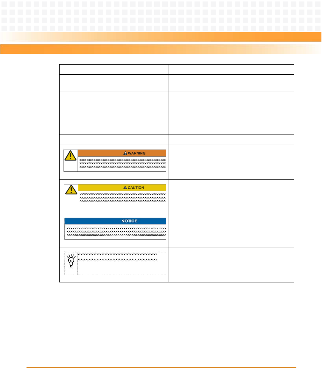
0,1,2,3, and 4 (used in registers)
Indicates a hazardous situation which, if not avoided,
could result in death or serious injury
Indicates a hazardous situation which, if not avoided,
may result in minor or moderate injury
18
Indicates a property damage message
No danger encountered. Pay attention to important
information
MVME3100 Single Board Computer Installation and Use (6806800M28C)
About this Manual
Summary of Changes
This manual has been revised and replaces all prior editions.
Part Number Publication Date Description
6806800M28C December 2012 Added Declaration of Conformity on page 22.
6806800M28B August 2011 Updated Safety Notes on page 148 and
Sicherheitshinweise on page 152.
6806800M28A April 2011 EA version
MVME3100 Single Board Computer Installation and Use (6806800M28C)
19

About this Manual
About this Manual
20
MVME3100 Single Board Computer Installation and Use (6806800M28C)

Hardware Preparation and Installation
1.1 Overview
The MVME3100 is a single-slot, single-board computer based on the MPC8540 PowerQUICC
III™ integrated processor. The MVME3100 provides serial ATA (sATA), USB 2.0, 2eSST VMEbus
interfaces, dual 64-bit/100 MHz PMC sites, up to 128MB of Flash, dual 10/100/1000 Ethernet,
one 10/100 Ethernet, and five serial ports. This board supports front and rear I/O and a single
SODIMM module for DDR memory. Access to rear I/O is available with the MVME721 rear
transition module (RTM).
Front-panel connectors on the MVME3100 board include: one RJ-45 connector for the Gigabit
Ethernet, one RJ-45 connector for the asynchronous serial port, one USB port with one type A
connector, one sATA port with one external sATA connector, and a combined reset and abort
switch.
Rear-panel connectors on the MVME721 board include: one RJ-45 connector for each of the
10/100 and 10/100/1000 BaseT Ethernets and four RJ-45 connectors for the asynchronous
serial ports. The RTM also provides two planar connectors for one PIM with rear I/O.
Chapter 1
1.2 Getting Started
This section provides an overview of the steps necessary to install and power up the
MVME3100 and a brief section on unpacking and ESD precautions.
1.2.1 Overview of Startup Procedures
The following table lists the things you will need to do before you can use this board and tells
where to find the information you need to perform each step. Be sure to read this entire
chapter, including all Caution and Warning notes, before you begin.
Table 1-1 Startup Overview
What you need to do... Refer to...
Unpack the hardware. Unpacking Guidelines on page 22
Identify various components on the board. MVME3100 Layout on page 23
Install the MVME3100 board in a chassis. on page 30
MVME3100 Single Board Computer Installation and Use (6806800M28C)
21
Hardware Preparation and Installation
Table 1-1 Startup Overview (continued)
What you need to do... Refer to...
Connect any other equipment you will be using Connecting to Peripherals on page 31
Verify the hardware is installed. Completing the Installation on page 33
1.2.2 Unpacking Guidelines
Unpack the equipment from the shipping carton. Refer to the packing list and verify that all
items are present. Save the packing material for storing and reshipping of equipment.
If the shipping carton is damaged upon receipt, request that the carrier’s agent be present
during the unpacking and inspection of the equipment.
Damage of Circuits
z Electrostatic discharge and incorrect installation and removal of the product can
damage circuits or shorten their life.
z Before touching the product make sure that your are working in an ESD-safe
environment or wear an ESD wrist strap or ESD shoes. Hold the product by its edges and
do not touch any components or circuits.
1.3 Declaration of Conformity
For Declaration of Conformity, refer MVME3100 Series Declaration of Conformity.
1.4 Configuring Hardware
This section discusses certain hardware and software tasks that may need to be performed
prior to installing the board in a chassis.
To produce the desired configuration and ensure proper operation of the MVME3100, you may
need to carry out certain hardware modifications before installing the module.
22
MVME3100 Single Board Computer Installation and Use (6806800M28C)

Hardware Preparation and Installation
Most options on the MVME3100 are software configurable. Configuration changes are made
by setting bits in control registers after the board is installed in a system.
Jumpers/switches are used to control those options that are not software configurable. These
jumper settings are described further on in this section. If you are resetting the board jumpers
from their default settings, it is important to verify that all settings are reset properly.
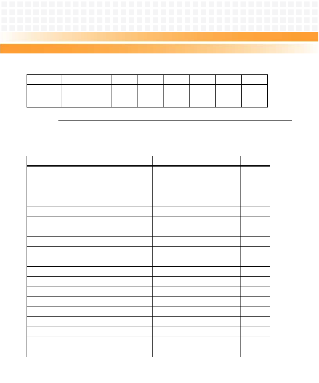
1.4.1 MVME3100 Layout
Figure 1-1 on page 25 illustrates the placement of the jumpers, headers, connectors, switches,
and various other components on the MVME3100.
There are two switch blocks which have user-selectable settings. Refer to Table 1-2, Tab le 1-3 ,
and Table 1-4 for switch settings. There is one switch on the MVME721. Refer to Table 1-5 and
Table 1-6 for switch settings.
MVME3100 Single Board Computer Installation and Use (6806800M28C)
23

Hardware Preparation and Installation
The MVME3100 is factory tested and shipped with the configuration described in the following
sections.
24
MVME3100 Single Board Computer Installation and Use (6806800M28C)
Hardware Preparation and Installation
Figure 1-1 Board Layout
J25 J24
J30J28
J2
J13 J14
J11 J12
J23
J21 J22
P1
P2
U21
J4
U1012
U1003
U1010
U5000
U1014
U1020
U1019
U1049
U1050
U1024
U1012
U1000
U1007
U1052
U1025
U1026
U1027
U1046
U1047
U1051
1
1
S4
S3
MVME3100 Single Board Computer Installation and Use (6806800M28C)
25
Hardware Preparation and Installation
1.4.2 Configuration Switch (S4)
An 8-position SMT configuration switch controls the VME SCON setting, Flash bank writeprotect, and the safe start ENV settings. It also selects the Flash boot image. The default setting
on all switch positions is OFF.
Table 1-2 Configuration Switch (S4) Settings
Setting
Switch Pos.
NotesOFF (Factory Default) ON
SAFE_START 1 Normal ENV settings
should be used.
BOOT BLOCK
SELECT
FLASH BANK WP 3 Entire Flash is not write-
Reserved 4
VME SCON
AUTO/MANUAL
MODE
MANUAL VME
SCON SELECT
Reserved 7
2 Flash memory map is
normal and boot block A
is selected.
protected.
5 Auto-SCON mode. Manual SCON mode. Manual SCON mode
6 Non-SCON mode. Always SCON mode. This switch is only
Safe ENV settings
should be used.
Boot block B is
selected and mapped
to the highest
address.
Flash is writeprotected.
This switch status is
readable from System
St atu s r egi st er 1 , b it 5.
Software may check
this bit and act
accordingly.
works in conjunction
with the VME SCON
SELECT switch.
effective when the
VME SCON
AUTO/MANUAL
MODE switch is ON.
26
MVME3100 Single Board Computer Installation and Use (6806800M28C)
Hardware Preparation and Installation
Table 1-2 Configuration Switch (S4) Settings (continued)
16
Not used
PCI-X mode
GAP#=0
GA4#=0
GA3#=0
GA2#=0
GA1#=0
GA0#=0
1
2
3
4
5
6
7
8
1
16
Not used
PCI-X mode
GAP#=1
GA4#=1
GA3#=1
GA2#=1
GA1#=1
GA0#=1
1
2
3
4
5
6
7
8
1
ONON
Factory Default
Setting
Switch Pos.
TRST SELECT 8 Normal MPC8540 TRST
mode where the board
HRESET will assert TRST.
Isolates the board
HRESET from TRST
and allows the board
to reset without
resetting the
MPC8540 JTAG/COP
interface.
1.4.3 Geographical Address Switch (S3)
The TSi148 VMEbus Status register provides the VMEbus geographical address of the
MVME3100. This switch reflects the inverted states of the geographical address signals.
Applications not using the 5-row backplane can use the geographical address switch to assign
a geographical address.
Figure 1-2 Geographical Address Switch Settings
NotesOFF (Factory Default) ON
This switch should
remain in the OFF
position unless a
MPC8540 emulator is
attached.
Table 1-3 Geographical Address Switch Assignments
Position SW1 SW2
Function Not
MVME3100 Single Board Computer Installation and Use (6806800M28C)
Used
1
PCI Bus
A mode
SW3 SW4 SW5 SW6 SW7 SW8
GAP GA4 GA3 GA2 GA1 GA0
27
Hardware Preparation and Installation
Table 1-3 Geographical Address Switch Assignments (continued)
PCI
mode
1
SW3 SW4 SW5 SW6 SW7 SW8
OFF
1
OFF
1
OFF
1
OFF
1
OFF
1
OFF
1
Position SW1 SW2
Fac to ry
Setting
(Default)
OFF OFF
Note:1SW2 has been configured to work in PCI-X mode only. The default setting is OFF.
Table 1-4 Slot Geographical Address Settings
Slot Address GAP GA(4:0) SW3 SW4 SW5 SW6 SW7 SW8
1 1 11110 OFF OFF OFF OFF OFF ON
2 1 11101 OFF OFF OFF OFF ON OFF
3 0 11100 ON OFF OFF OFF ON ON
4 1 11011 OFF OFF OFF ON OFF OFF
5 0 11010 ON OFF OFF ON OFF ON
6 0 11001ONOFFOFFONONOFF
7 1 11000 OFF OFF OFF ON ON ON
8 1 10111 OFF OFF ON OFF OFF OFF
9 0 10110 ON OFF ON OFF OFF ON
10 0 10101 ON OFF ON OFF ON OFF
11 1 10100 OFF OFF ON OFF ON ON
12 0 10011 ON OFF ON ON OFF OFF
13 1 10010 OFF OFF ON ON OFF ON
14 1 10001 OFF OFF ON ON ON OFF
15 0 10000 ON OFF ON ON ON ON
16 1 01111 OFF ON OFF OFF OFF OFF
17 0 01110 ON ON OFF OFF OFF ON
18 0 01101 ON ON OFF OFF ON OFF
19 1 01100 OFF ON OFF OFF ON ON
28
MVME3100 Single Board Computer Installation and Use (6806800M28C)
Hardware Preparation and Installation
Table 1-4 Slot Geographical Address Settings (continued)
Slot Address GAP GA(4:0) SW3 SW4 SW5 SW6 SW7 SW8
20 0 01011 ON ON OFF ON OFF OFF
21 1 01010 OFF ON OFF ON OFF ON
1.4.4 PMC I/O Voltage Configuration
The onboard PMC sites may be configured to support 3.3V or 5.0V I/O PMC modules. To
support 3.3V or 5.0V I/O PMC modules, both PMC I/O keying pins must be installed in the
holes. If both keying pins are not in the same location or if the keying pins are not installed, the
PMC sites will not function. Note that setting the PMC I/O voltage to 5.0V forces the PMC sites
to operate in PCI mode instead of PCI-X mode. The default factory configuration is for 3.3V
PMC I/O voltage.
1.4.5 RTM SEEPROM Address Switch (S1)
A 4-position SMT configuration switch is located on the RTM to set the device address of the
RTM serial EEPROM device. The switch settings are defined in the following table.
Table 1-5 RTM EEPROM Address Switch Assignments
Position SW1 SW2 SW3 SW4
Function A0 A1 A2 Not Used
OFF 1 1 1
Table 1-6 EEPROM Address Settings
Device Address A(2:0) SW1 SW2 SW3
$A0 000 ON ON ON
$A2 001 OFF ON ON
$A4 010 ON OFF ON
$A6 011 OFF OFF ON
$A8 100 ON ON OFF
$AA (Factory) 101 OFF ON OFF
MVME3100 Single Board Computer Installation and Use (6806800M28C)
29
Hardware Preparation and Installation
Table 1-6 EEPROM Address Settings (continued)
Device Address A(2:0) SW1 SW2 SW3
$AC 110 ON OFF OFF
$AE 111 OFF OFF OFF
The RTM EEPROM address switches must be set for address $AA in order for this device to be
accessible by MotLoad.
1.5 Installing Hardware
Damage of the Product and Additional Devices and Modules
z Incorrect installation or removal of additional devices or modules may damage the
product or the additional devices or modules.
z Before installing or removing additional devices or modules, read the respective
documentation.
Damage of Circuits
z Electrostatic discharge and incorrect installation and removal of the product can
damage circuits or shorten their life.
z Before touching the product make sure that your are working in an ESD-safe
environment or wear an ESD wrist strap or ESD shoes. Hold the product by its edges and
do not touch any components or circuits.
Product Malfunction
z Switches marked as “Reserved” might carry production-related functions and can
cause the product to malfunction if their setting is changed.
z Do not change settings of switches marked as “reserved”.
30
MVME3100 Single Board Computer Installation and Use (6806800M28C)
Loading...