Diodes ES3A, ES3AB, ES3D, ES3DB User Manual

Features
•Glass Passivated Die Construction
•Super-Fast Recovery Time For High Efficiency
•Surge Overload Rating to 100A Peak
•Ideally Suited for Automated Assembly
•Lead Free Finish/RoHS Compliant (Note 1)
•Green Molding Compound (No Halogen and Antimony) (Note 2)
|
|
ES3A/AB - ES3D/DB |
Green |
||
|
|
|
3.0A SURFACE MOUNT SUPER-FAST RECTIFIER
Mechanical Data
•Case: SMB/SMC
•Case Material: Molded Plastic. UL Flammability Classification Rating 94V-0
•Moisture Sensitivity: Level 1 per J-STD-020
•Terminals: Lead Free Plating (Matte Tin Finish). Solderable per MIL-STD-202, Method 208 
•Polarity: Cathode Band or Cathode Notch
•SMB Weight: 0.093 grams (approximate)
•SMC Weight: 0.21 grams (approximate)
Top View |
Bottom View |
Ordering Information (Note 3)
Part Number |
Case |
Packaging |
ES3x-13-F |
SMC |
3000/Tape & Reel |
ES3xB-13-F |
SMB |
3000/Tape & Reel |
* x = Device type, e.g. ES3A-13-F (SMC package); ES3AB-13-F (SMB package).
Notes: |
1. |
EU Directive 2002/95/EC (RoHS). All applicable RoHS exemptions applied, see EU Directive 2002/95/EC Annex Notes. |
|
2. |
Product manufactured with Data Code 0924 (week 24, 2009) and newer are built with Green Molding Compound. |
|
3. |
For packaging details, go to our website at http://www.diodes.com. |
Marking Information
 YWW
YWW
ES3x(B)
ES3x = Product type marking code, ex: ES3A (SMC package) ES3xB = Product type marking code, ex: ES3AB (SMB package)  = Manufacturers’ code marking
YWW = Date code marking
Y = Last digit of year (ex: 2 for 2002) WW = Week code (01 to 53)
ES3A/AB - ES3D/DB |
1 of 4 |
November 2010 |
Document number: DS14003 Rev. 15 - 2 |
www.diodes.com |
© Diodes Incorporated |

ES3A/AB - ES3D/DB
Maximum Ratings @TA = 25°C unless otherwise specified
Single phase, half wave, 60Hz, resistive or inductive load.
For capacitance load, derate current by 20%.
Characteristic |
|
Symbol |
ES3A/AB |
ES3B/BB |
|
ES3C/CB |
ES3D/DB |
Unit |
Peak Repetitive Reverse Voltage |
|
VRRM |
|
|
|
|
|
|
Working Peak Reverse Voltage |
|
VRWM |
50 |
100 |
|
150 |
200 |
V |
DC Blocking Voltage (Note 4) |
|
VR |
|
|
|
|
|
|
RMS Reverse Voltage |
|
VR(RMS) |
35 |
70 |
|
105 |
140 |
V |
Average Rectified Output Current |
@ TT = 100°C |
IO |
|
3.0 |
|
|
A |
|
Non-Repetitive Peak Forward Surge Current 8.3ms |
|
IFSM |
|
100 |
|
|
A |
|
Single Half Sine-Wave Superimposed on Rated Load |
|
|
|
|||||
|
|
|
|
|
|
|
||
Thermal Characteristics
|
|
Characteristic |
|
Symbol |
|
Value |
Unit |
|
|
Typical Thermal Resistance, Junction to Terminal |
|
RθJT |
|
10 |
°C/W |
|
|
|
|
|
|
|
|
|
||
|
Typical Thermal Resistance, Junction to Ambient (Note 5) |
RθJA |
|
50 |
° |
|
||
|
|
|
|
|
|
C |
|
|
|
Operating and Storage Temperature Range |
|
TJ, TSTG |
|
-55 to +150 |
°C |
|
|
|
|
|
|
|
|
|
||
|
|
|
|
|
||||
|
Electrical Characteristics @TA = 25°C unless otherwise specified |
|
|
|
||||
|
|
|
|
|
|
|
|
|
|
|
Characteristic |
|
Symbol |
|
Value |
Unit |
|
|
Maximum Forward Voltage |
@ IF = 3.0A |
VFM |
|
0.9 |
V |
|
|
|
|
|
|
|
|
|
|
|
|
Peak Reverse Current |
@ TA = 25°C |
IRM |
|
10 |
μA |
|
|
|
at Rated DC Blocking Voltage (Note 4) |
@ TA = 125°C |
|
500 |
|
|||
|
|
|
|
|
||||
|
Maximum Reverse Recovery Time (Note 6) |
|
trr |
|
25 |
ns |
|
|
|
|
|
|
|
|
|
|
|
|
Typical Total Capacitance (Note 7) |
|
CT |
|
45 |
pF |
|
|
|
|
|
|
|
|
|
|
|
|
Notes: |
4. Short duration pulse test used to minimize self-heating effect. |
|
|
|
|
|
|
5.Unit mounted on PC board with 5.0 mm2 (0.013 mm thick) copper pads as heat sink.
6.Measured with IF = 0.5A, IR = 1.0A, Irr = 0.25A. See Figure 5.
7.Measured at 1.0MHz and applied reverse voltage of 4.0V DC.
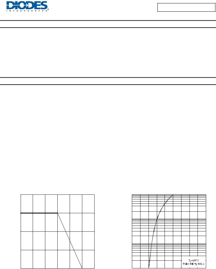
IO, AVERAGE RECTIFIED CURRENT (A)
4
Note 3
3
2
1
0
25 |
50 |
75 |
100 |
125 |
150 |
175 |
|
TT, TERMINAL TEMPERATURE (° C) |
|
||||
|
Fig. 1 |
Forward Current Derating Curve |
|
|||
CURRENT (A) |
10 |
|
|
|
|
|
|
|
|
|
|
FORWARD |
1.0 |
|
|
|
|
|
|
|
|
|
|
, INSTANTANEOUS |
0.1 |
|
|
|
|
|
|
|
|
|
|
F |
0.01 |
|
|
|
|
I |
|
|
|
|
|
|
0.4 |
0.8 |
1.2 |
1.6 |
|
|
0 |
||||
|
|
VF, INSTANTANEOUS FORWARD VOLTAGE (V) |
|||
|
|
Fig. 2 Typical Forward Characteristics |
|||
ES3A/AB - ES3D/DB |
2 of 4 |
November 2010 |
Document number: DS14003 Rev. 15 - 2 |
www.diodes.com |
© Diodes Incorporated |
 Loading...