Page 1
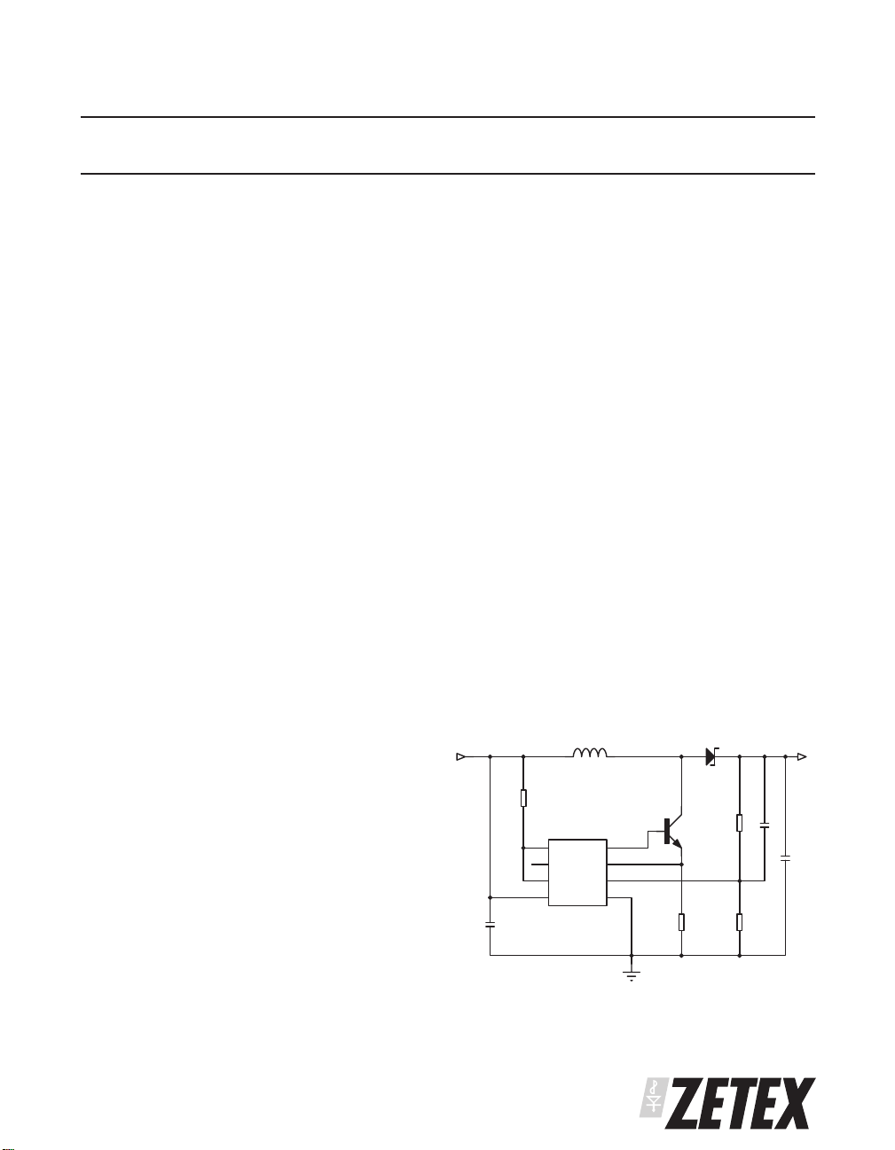
SINGLE CELL DC-DC CONVERTER SOLUTION
DESCRIPTION
The ZXSC100 series is designed for DC-DC
applications where step-up voltage conversion from
very low input voltages is required. These applications
mainly operate from single nickel cadmium or nickel
metal hydride battery cells.
The ZXSC100 devices are non-synchronous PFM,
DC-DC controller ICs which drive an external
transistor. Zetex SuperSOT4
with saturation resistance as low as 13mΩ, are
recommended as the external switching element.
These bipolar transistors are the best switching
devices available for this type of DC-DC conversion,
enabling high efficiency conversion with input
voltages down to below 1 volt.
The circuit can start up under full load with regulation
maintained down to an input voltage of only 0.926
volts. The solution configuration ensures optimum
™
switching transistors,
ZXSC100
efficiency over a wider range of load currents, several
circuit configurations are possible with power
dissipation up to 2W. The step up output voltage is
easily programmed with external resistors, the
non-synchronous architecture and SuperSOT4™
device enabling an output voltage down to the input
voltage level. For best performance the ZXSC100
quiescent current isasmall 150µA ensuring minimum
battery drain in no load conditions.
For the best in space saving theZXSC100 is offered in
the MSOP8 package, however the devices are also
available in SO8 packaging for applications where
space saving is not so critical.
The IC and discrete combination offers the ultimate
cost vs performance solution for single cell DC-DC
conversion.
FEATURES
• SuperSOT4™ switching transistor
ZXT14N20DX:V
45mV max @ 1A load
CE(sat)
• Efficiency maintained over a wide range of input
voltages and load currents
82% efficiency @ V
•
Startup under full load
•
Minimum operating input voltage V
•
Adjustable output voltage down to V
•
Quiescent current typically 150µA referred to
input voltage
•
MSOP8 Package
•
SO8 Package
•
Demonstration boards available
BATT
=1V
BATT
BATT
=0.926V
APPLICATIONS
•
Cordless Telephones
•
MP3 Players
•
PDA
•
Pagers
•
Battery Backup Supplies
•
Electronic toothbrush
•
GPS Receivers
•
Digital Camera
•
Palmtop Computers
APPLICATIONS(continued)
• Hand Held Instruments
• Portable Medical Equipment
• Solar Powered Equipment
• LED Flashlight
•
LED Backlight
TYPICAL APPLICATION CIRCUIT
V
BATT
C1
L1 D1
R1
U1
V
EM
DRIVE
I
BAS
SENSE
RE
FB
V
G
CC
ND
ZXSC100
ZHCS2000
Q1
ZXT14N20DX
R2
3.3V/0.1A
R3
C3
C2
R4
ISSUE 1 - JANUARY 2001
1
Page 2

ZXSC100
ABSOLUTE MAXIMUM RATING
Supply Voltage 0.3 to 3.5V
Maximum Voltage Other Pins 0.3 to V
CC
+0.3V
Power Dissipation
MSOP8 500mW
SO8 780mW
ELECTRICAL CHARACTERISTICS TEST CONDITIONS (Unless otherwise stated)
=1.2V, TA= 25°C
V
CC
Symbol Parameter Conditions Min Typ Max Units
I
CC
I
DRIVE
V
DRIVE
V
FB
V
ISENSE
Quiescent current Not switching 150 200 µA
Base drive current VRE=V
V
o/p voltage VRE=VCC,I
DRIVE
Feedback voltage 708 730 752 mV
Output current
reference voltage
Operating Temperature 0 to 70°C
Storage Temperature -55 to 125°C
Junction Temperature 150°C
CC
= 5mA VCC- 0.17 V
DRIVE
510mA
12 17.5 24 mV
T
CVISENSEISENSE
V
DREF
T
CVDREF
V
CC(SRT)
V
CC(min)
V
CC(hys)
I
FB
I
ISENSE
V
O(min)
V
O(max)
1
Depends on breakdown voltage of pass device. See ZXT14N20DX data sheet
voltage temp co. 0.4 %/°C
Drive current reference
voltage
V
temp co. 1 %/°C
DREF
Measured with respect
to V
CC
20 30 40 mV
Startup voltage Any output load 1.01 1.06 1.1 V
Minimum operating
0.926 0.98 1 V
input voltage
Supply start up to
shutdown hysteresis
Feedback input current 100 200 nA
I
input current V
SENSE
Minimum Output
Voltage
Maximum Output
Voltage
ZXT14N20DX as pass
element
= 0V 3 4 5.5 µA
ISENSE
V
CC
1
80 mV
V
20 V
ISSUE 1 - JANUARY 2001
2
Page 3
ZXSC100
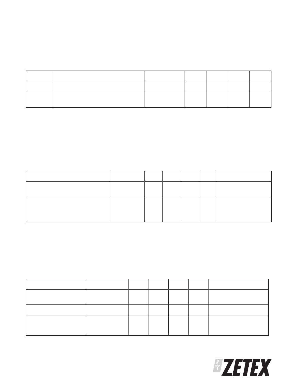
ELECTRICAL CHARACTERISTICS: AC PARAMETERS
2
TEST CONDITIONS (Unless otherwise stated) )
V
=1.2V, TA= 25°C
CC
Symbol Parameter Conditions Min Typ Max Units
T
OFF
F
OSC
2
These parameters guaranteed by Design
3
Operating frequency is application circuit dependant. See applications section
Discharge Pulse Width 1.7 3 4 µs
Recommended operating
frequency
3
200 kHz
ZXT14N20DX
For the circuits described in the applications section, Zetex ZXT14N20DX is the recommended pass transistor.
The following indicatesoutlinedata for the ZXT,moredetailed information can befoundin the Zetex SuperSOT4
data book or at www.zetex.com
ELECTRICAL CHARACTERISTICS (at TA= 25°C unless otherwise stated).
PARAMETER SYMBOL MIN. TYP. MAX. UNIT CONDITIONS.
Collector-Emitter Breakdown
Voltage
Collector-Emitter Saturation
Voltage
V
(BR)CEO
V
CE(sat)
20 30 V IC=10mA*
4.5
30
75
45
95
6
mV
mV
mV
IC=0.1A, IB=10mA*
I
=1A, IB=10mA*
C
I
=4A, IB=40mA*
C
*Measured under pulsed conditions. Pulse width=300µs. Duty cycle ≤2%
ZHCS2000
For the circuits described in the applications section Zetex ZHCS2000 is the recommended Schottky diode. The
following indicates outline data for the ZHCS, more detailed information is available at www.zetex.com
ELECTRICAL CHARACTERISTICS (at T
PARAMETER SYMBOL MIN. TYP. MAX. UNIT CONDITIONS.
Forward Voltage V
Reverse Current I
Reverse Recovery
Time
*Measured under pulsed conditions. Pulse width=300µs. Duty cycle ≤2%
ISSUE 1 - JANUARY 2001
F
R
t
rr
= 25°C unless otherwise stated).
amb
385
500mVmV
300
µA
5.5 ns Switched from IF=
3
3
IF=1A
I
=2A
F
VR=30V
500mA to I
Measured at I
R
= 500mA.
=50mA
R
Page 4
ZXSC100
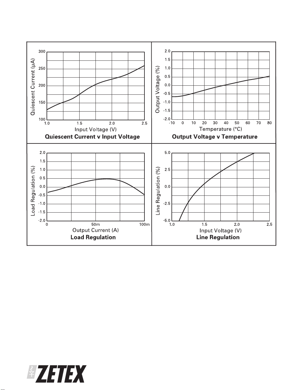
TYPICAL CHARACTERISTICS
ISSUE 1 - JANUARY 2001
4
Page 5
ZXSC100
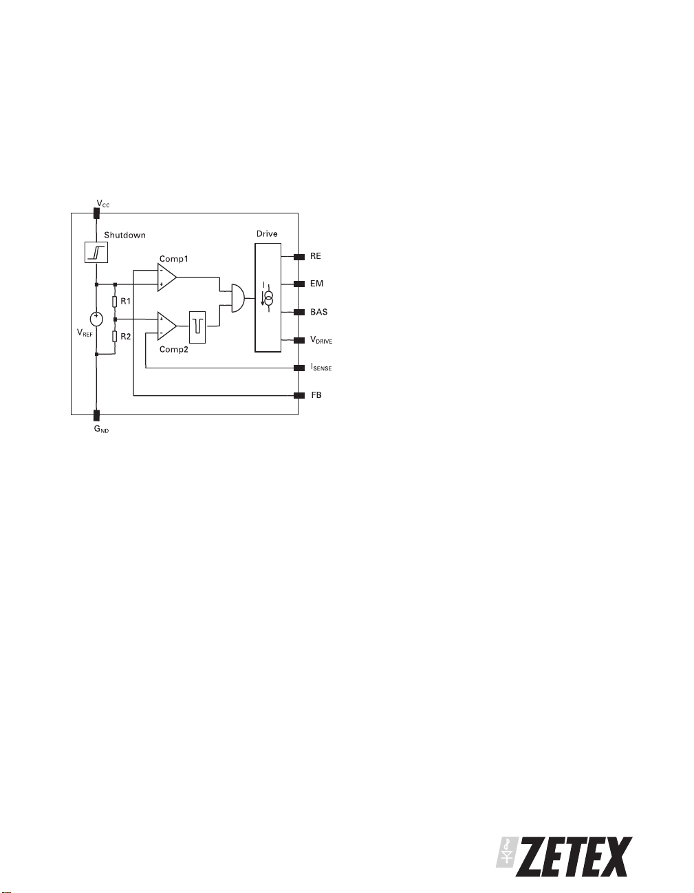
DEVICE DESCRIPTION
The ZXSC100 is non-synchronous PFM, DC-DC
controller IC which, when combined with a high
performance external transistor, enables the
production ofa high efficiencyboost converter for use
in single cell applications. A block diagram is shown
for the ZXSC100 in Figure 1.
Figure 1
ZXSC100 Block Diagram
A shutdown circuitturnsthe device on oroffat V
with a hysteresis of typically 80mV. At start up,
comparator Comp1 turns the driver circuit and
therefore the external switching transistor on. This
circuit will remain active until the feedback voltage at
the pin FB rises above V
, which is set to 730mV. An
REF
external resistive divider on the FB pin sets the output
voltage level.
Comparator Comp2 forces the driver circuit and the
external switching transistor off, if the voltage at
I
exceeds 25mV. The voltage at I
SENSE
SENSE
from a current sense resistor connected in series with
the emitter of the switching transistor.
A monostable following the output of Comp2 extends
the turn-off time of the output stage by a minimum of
2us. This ensures that there is sufficient time to
discharge the inductor coil before the next on period.
The AND gate between the monostable and Comp1
output ensures that the switching transistor always
remains on until the I
threshold is reached and
SENSE
that the minimum discharge period is always
asserted. The pulse width is constant, the pulse
frequency varies with the output load.
=1V
CC
is taken
The driver circuit supplies the external switching
transistor with a defined current, which is
programmed by an external resistor connected
between the RE pin and V
voltage for thecircuitis 25mV below V
. The internal reference
CC
. To maximise
CC
efficiency the external transistor is switched quickly,
typically being forced off within 20ns.
In higher power applications more current can be
supplied to the switching transistor by using a further
external component. Thedriver transistor in theICcan
be bypassedwiththe addition ofa discrete PNP. More
information on this circuit configuration can be found
in the applications section.
ISSUE 1 - JANUARY 2001
5
Page 6
ZXSC100
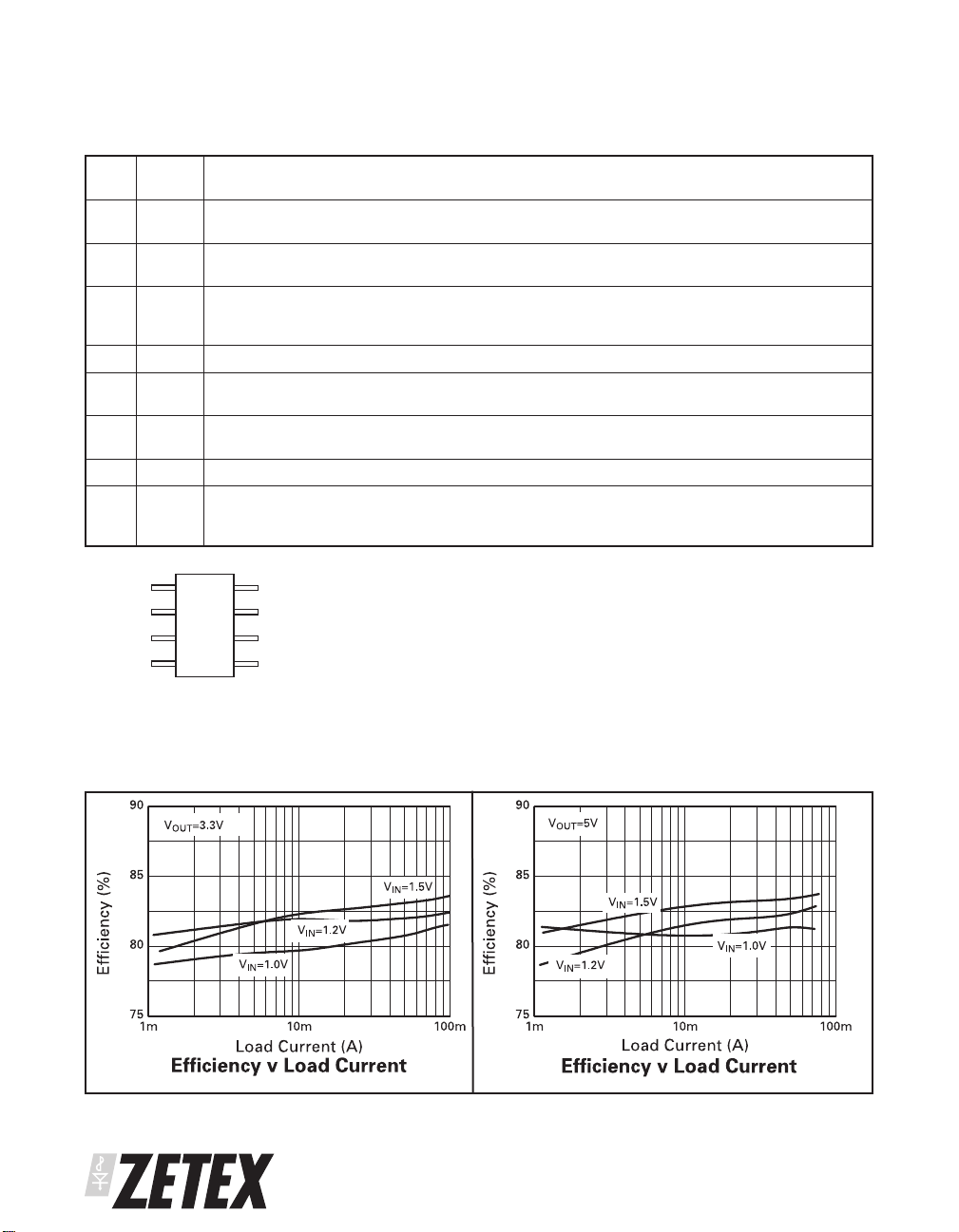
PIN DESCRIPTIONS
Pin
Name Description
No.
1 EM Emitter of internal drive transistor. Connect to RE in lower power applications.
2 BAS Not connected in lower power applications. Connect to base of external drive
3 RE Drive current sense input. Internal threshold voltage set 25mV below V
4V
5I
CC
SENSE
6 FB Feedback sense. Internal threshold set to 730mV. Connect external resistive
7G
8V
DRIVE
Must be unconnected in higher power applications
transistor in higher power applications
Connected external sense resistor. Connect emitter of external drive transistor in
higher power applications
Supply voltage, generally NiMH, NiCd single cell
Inductor current sense input. Internal threshold voltage set to 25mV. Connect
external sense resistor
divider to output voltage
Ground
ND
Drive output for external switching transistor. Connect to base of external
switching transistor. Also connect to collector of external drive transistor in
higher power applications
CC
.
EM
BAS
RE
V
CC
1
2
3
4
V
8
DRIVE
G
7
ND
FB
6
5
I
SENSE
REFERENCE DESIGNS
Three typical DC-DC step-up converter applications
for the ZXSC100 are shown. Firstly with a maximum
output power of 0.33W, secondly with a maximum
Low Power Solution (330mW) Efficiency
output power of1.0Wand finally driving whiteLED’sin
a flashlight application.
ISSUE 1 - JANUARY 2001
6
Page 7

ZXSC100
Low power solution, V
=3.3V, PL=0.33W
OUT
V
BATT
C1
L1 D1
R1
U1
V
EM
DRIVE
BAS
I
SENSE
RE
FB
V
G
CC
ND
ZXSC100
ZHCS2000
Q1
ZXT14N20DX
R2
R3
R4
Materials list
Ref Value Part Number Manufacturer Comments
U1 N/A ZXSC100X8 Zetex Plc Single cell converter, MSOP8
Q1
20V, 13mΩ,7A
ZXT14N20DX Zetex Plc Low VCE(sat) NPN, MSOP8
D1 0.5V, 2A ZHCS2000 Zetex Plc 2A Shottky diode
R1
R2
0Ω*
33mΩ
Generic Various 0805 Size
Generic Various 0805 Size
3.3V/0.1A
C3
C2
R3
R4
110kΩ
30kΩ
Generic Various 0805 Size
Generic Various 0805 Size
C1 220µF TPSD227M010R0100 AVX Low ESR tantalum capacitor
C2 220µF TPSD227M010R0100 AVX Low ESR tantalum capacitor
C3 1nF Generic Various 0805 Size
L1 22µH D01608C-223
Coilcraft Low profile SMT
D03316P-223
* Note: Refer to External Transistor base drive selection in the Applications Section.
ISSUE 1 - JANUARY 2001
7
Page 8

ZXSC100
Higher power solution, V
V
BATT
R1
C1
L1 D1
U1
V
EM
DRIVE
I
BAS
SENSE
FB
RE
V
G
CC
ND
ZXSC100
OUT
Q2
=3.3V, PL=1W
3.3V/0.33A
ZHCS2000
Q1
ZXT14N20DX
R2
C3
R3
R4
C2
Materials list
Ref Value Part Number Manufacturer Comments
U1 N/A ZXSC100X8 Zetex Plc Single cell converter, MSOP8
Q1
20V, 13mΩ,7A
ZXT14N20DX Zetex Plc Low VCE(SAT) NPN, MSOP8
Q2 N/A 2N2907 Various Small signal transistor
D1 0.5V, 2A ZHCS2000 Zetex Plc 2A Shottky diode
R1
R2
R3
R4
3.3Ω*
33mΩ
110kΩ
30kΩ
Generic Various 0805 Size
Generic Various 0805 Size
Generic Various 0805 Size
Generic Various 0805 Size
C1 220µF TPSD227M010R0100 AVX Low ESR tantalum capacitor
C2 220µF TPSD227M010R0100 AVX Low ESR tantalum capacitor
C3 1nF Generic Various 0805 Size
L1 22µH D01608C-223
Coilcraft Low profile SMT
D03316P-223
* Note: Refer to External Transistor base drive selection in the Applications Section.
ISSUE 1 - JANUARY 2001
8
Page 9

ZXSC100
OTHER APPLICATIONS
Driving white LED’s in a flashlight application
U1
EM
BAS
RE
V
CC
ZXSC100
L1
100µH
V
DRIVE
I
SENSE
Q1
ZXT13N15
FB
G
ND
R2
0.22R
D1
WHITE LED
V
BATT
The ZXSC100 solution is ideal for LED lamp driving
applications operating from a single cell. In principal
conversion from 1.2V to the 3.6V, typically required by
white LEDs, is necessary. Load currents in the region of
20mA to 50mA being required for a singleLEDelement.
To minimise size, weight and cost, single cell operation
is anadvantage. The ZXSC is well matched to singlecell
NiCd and NiMHcharacteristics.Thecircuitwillturn on at
1.06V, to maximise the life the battery can offer, the
converter does not turn off until the batteryvoltage falls
to 0.93V.
The circuit itself is very simple, a minimum number of
components are used and they are all small size. The
ZXSC uses the very smallMSOP8 package, the pass
transistor is SOT23. No capacitors are required as
the circuit is stable under all conditions. The inductor
recommended is a low cost miniature component.
No compromise is made on efficiency however. In a
standard configuration efficiency well over 80% can
be achieved. With careful inductor selection
efficiency over 90% is possible.
The inherent flexibility of the ZXSC circuit means
that parallel or series LEDs can be driven depending
on application needs. A simple modification to the
application circuit means that the maximum pulse
current can be programmed to match the
characteristics ofthe chosen LED load,pulse current
in the range 10mA to 3A and beyond can be easily
achieved.
An application note (AN33) is available describing
various circuits for driving white LEDs. This
application note includes details of circuits that
optimise battery life, maximise brightness and can
be constructed for minimal cost. Contact your local
Zetex office for further details.
ISSUE 1 - JANUARY 2001
9
Page 10

ZXSC100
APPLICATIONS INFORMATION
The following section is a design guide for optimum
converter performance.
Switching transistor selection
The choice of switching transistor has a major impact
on the DC-DC converter efficiency. For optimum
performance, a bipolar transistor with low V
and highgain is required.The majority oflosses in the
transistor are, ‘on-state’ and can be calculated by
using the formula below:
((I xV I x V ))xT
AV CE(SAT) B BE(SAT) ON
P
=
Q1
where
I
=
AV
I
2
PK
++)(
(T T
ON OFF)
)
From the calculations above the impact on converter
efficiency can be seen.
The Zetex ZXT14N20DX is an ideal choice of
transistor, having the lowest saturation voltage in its
class. A datasheetfortheZXT14N20DX is available on
the Zetex web site or through your local Zetex sales
office. Outline information is included in the
characteristics section of this data sheet.
ZXT14N20DX Saturation Characteristic.
CE(SAT)
ZXT14N20DX Saturation Characteristic.
External drive transistor selection
For higherpower applications anexternal transistor is
required to provide the additional base drive current
to the main switching transistor. For this, any small
signal PNP transistor is sufficient. Please seereference
designs for recommended part numbers.
Schottky diode selection
As with the switching transistor the Schottky rectifier
diode has a major impact on the DC-DC converter
efficiency. A Schottky diode with a low forward
voltage and fast recovery time should be used for this
application. The majority of losses in the diode are,
‘on-state’ and can be calculated by using the formula
below:
IxV xT
AV F(MAX) DIS
P
=
D1
(T T
+ )
On OFF
I
where
PK
I
=
AV
2
The diode should be selected so that the maximum
forward current is greater or equal to the maximum
peak current in the inductor, and the maximum
reverse voltage is greater or equal to the output
voltage.
The Zetex ZHCS2000 meets these needs. A data sheet
for the ZHCS2000 is available on the Zetex web site or
through your local Zetex sales office. Outline
information is included in the characteristics section of
this data sheet.
10
ISSUE 1 - JANUARY 2001
Page 11

ZXSC100
Inductor selection
The inductor value must be chosen to satisfy
performance, cost and size requirements of theoverall
solution. Forthe referencedesigns we recommend an
inductor value of 22µH with a core saturation current
rating greater than the converter peak current value.
Inductor selection has a significant impact on the
converter efficiency.For applications where efficiency
is critical, a 5% improvement can be achieved with a
high performance inductor. This should be selected
with acore saturation current ratingmuch higher than
the peak current of the converter, say 3 times greater.
The resultant reductionincore losses brings about the
efficiency improvement.
Peak current definition
The peak current rating is a design parameter whose
value is dependent upon the overall application. For
the reference designs, a peak current of 1.2A was
chosen to ensure that the converter could provide the
required output power.
In general,the I
value mustbe chosento ensure that
PK
the switching transistor, Q1, is in full saturation with
maximum output power conditions, assuming
worse-case input voltage and transistor gain under all
operating temperature extremes.
Once I
is decided the value of R
PK
SENSE
can be
determined by:
V
R
SENSE
ISENSE
=
I
PK
Output power definition
By making the above assumptions for the inductor and
the output power can be determined by:
I
PK
(V V x I x T
−+)
Output Power
OUT IN PK DIS
=
2x(T T
On OFF
)
where
IxL
PK
T
=
ON
V
IN
and
IxL
T
DIS
Note: V
PK
=
VV
−()
OUT IN
= output voltage + rectifier diode VF
OUT
Figure 3 shows the discontinuous inductor current and
the relationship between output power, T
T
.
OFF
Figure 3
Discontinuous inductor current
ON,TDIS
and
Output capacitors
Output capacitors are a critical choice in the overall
performance of thesolution.They are required to filter
the output and supply load transient currents. There
are three parameters which are paramount in the
selection of the output capacitors; their capacitance
value, I
and ESR. The capacitance value is
RIPPLE
selected to meet theload transient requirements. The
capacitors I
rating must meet or exceed the
RIPPLE
current ripple of the solution.
The ESR of the output capacitor can also affect loop
stability and transient performance. The capacitors
selected for the solution, and indicated in the
reference designs, are optimised to provide the best
overall performance.
ISSUE 1 - JANUARY 2001
11
Page 12

ZXSC100
Input capacitors
The input capacitor is chosen for its voltage and RMS
current rating. The use of low ESR electrolytic or
tantalum capacitors is recommended. Capacitor
values foroptimum performanceare suggested in the
reference design section.
Also note that the ESR of the input capacitor is
effectively in series with the input and hence
contributes to efficiency losses in the order of I
RMS
2
ESR.
Output voltage adjustment
The ZXSC100 is an adjustable converter allowing the
end user the maximum flexibility in output voltage
selection. For adjustable operation a potential divider
network is connected as indicated in the diagram.
The output voltage is determined by the equation:
V
= VFB(1 + RA / RB),
OUT
where V
=730mV
FB
The resistor values, RA and RB, should be maximised
to improve efficiency and decrease battery drain.
Optimisation can be achieved by providing a
minimum current of I
The output is adjustable from V
=200nA to the V
FB(MAX)
to the (BR)V
FB
BATT
CEO
pin.
of
the switching transistor, Q1.
Note: For the reference designs, RA is assigned the
label R3 and RB the label R4.
V
OUT
RA
V
x
FB
RB
0V
External Transistor base drive selection
Optimisation of the external switching transistor base
drive may be necessaryfor improved efficiency in low
power applications. This can be achieved by
introducing an external resistor between the supply
and the RE pin of the ZXSC100. The resistor value can
be determined by:
V
DREF
R
=
1
I
B
1212
ISSUE 1 - JANUARY 2001
Page 13

ZXSC100
Layout issues
Layout is critical for the circuit tofunction optimally in
terms of electrical efficiency, thermal considerations
and noise.
For ‘step-up converters’ there are four main current
loops, the inputloop,power-switch loop, rectifier loop
and output loop. The supply charging the input
capacitor forms theinputloop. The power-switch loop
is defined when Q1 is‘on’,currentflowsfromtheinput
through theinductor,Q1, R
Q1 is ‘off’, the energy stored in the inductor is
transferred to the output capacitor and load via D1,
forming the rectifier loop. The output loop is formed
by the output capacitor supplying the load when Q1 is
switched back off.
To optimise for best performance each of these loops
should be kept separate from each other and
interconnections made with short, thick traces thus
and toground.When
SENSE
minimising parasitic inductance, capacitance and
resistance. Also the sense resistor R2 should be
connected, with minimum trace length, between
emitter leadof Q1 and ground,again minimising stray
parasitics.
The layout for the 0.33W solution is shown below.
Demonstration board
A demonstration board for the 0.33W solution, is
available upon request. These can be obtained
through your local Zetex office or through Zetex web
pages. For all reference designs, Gerber files and bill
of materials can be supplied.
Actual Size
Top Silk
Top Copper
0.33W solution demo board layout
ISSUE 1 - JANUARY 2001
Drill Holes
Bottom Copper
13
Page 14

ZXSC100
Designing with the ZXSC100.
Introduction
This section refers to the ZXSC100, 3.3V/100mA
output reference design and demonstrates the
dynamic performance of the solution.
Figure 1.
ZXSC100 low power solution, 3.3V/100mA output.
Efficiency
Efficiency is oftenquotedasone of the key parameters
of a DC-DC converter. Not only does it give an
instantaneous idea of heat dissipation, but also an
idea as to the extent battery life can be extended.
Figure 2. Shows the efficiency of the ZXSC100 low
power solution. Efficiency v Output current is shown
for a 3.3V output at various input voltages.
Main switching waveforms
Steady state operation under constant load gives an
excellent indication of ZXSC100 performance.
Represented in Figure 3. is the main switching
waveform, measured at the collectorof Q1, indicating
the transistor on-state and the diode energy transferto
the output.
Figure 3.
Switching waveform
The peak switching current is derived from the
threshold of theI
(see Applications section for calculations). Figure 4.
shows the switching waveform associated with the
I
pin
SENSE
pin and thesenseresistor value
SENSE
Figure 2.
ZXSC100 efficiency v output current
Figure 4.
I
14
SENSE
threshold
ISSUE 1 - JANUARY 2001
Page 15

Shown in Figure 5. is the discontinuous inductor
current. The ramp-up current stores energy in the
inductor. The switching transistor,Q1,isonduringthis
time andhas an equivalent currentramp-up, shown in
Figure 6. The ramp-down current is associated with
the energy being delivered to the output via the
Schottky diode, D1. The diode current is equivalent to
this ramp-down current and is shown in figure 7.
Figure 5.
Inductor current (200mA/div)
Figure 7.
Diode current (200mA/div)
ZXSC100
Figure 6.
Transistor current (200mA/div)
ISSUE 1 - JANUARY 2001
15
Page 16

ZXSC100
Output Voltage Ripple
Output voltage ripple is shown in Figure 8. The circuit
is operated with a 1.2V input voltage, 3.3V output
voltage and 100mA load current. Output voltageripple
will be dependent, to a large extent, on the output
capacitor ESR. (see Applications section for
recommended capacitors).
Figure 8. Output voltage ripple for 3.3V/100mA
output.
Transient response
Transient response to step changes in load is a critical
feature in many converter circuits. The ZXSC100
operates a pulse by pulse regulation scheme and
therefore corrects for changes in the output every
pulse cycle, giving excellent response characteristic.
Measurement with a power supply
When measuring with a power supply it is important
to realise thattheimpedanceis much greater than that
of a secondary battery (NiCd or NiMH). To simulatethe
lower impedance of the battery x10 low ESR 1000uF
capacitors where placed in parallel at the input of the
converter. All the dynamic performance
measurements were taken using this technique.
ISSUE 1 - JANUARY 2001
16
Page 17

Supplier Listing
Zetex
AVX
Coilcraft
Sanyo Electronic
Comp. (OS-CON)
ZXSC100
GERMANY ASIA USA UK
Zetex GmbH
Munich
(49) 894549490 (852) 2610 0611 (1) 631 543 7100 (44) 161 622 4444
http://www.zetex.com
http://www.avxcorp.com
http://www.coilcraft.com
Sanyo Europe
Munich
(49) 89 457693 16
http://www.sanyovideo.com
Zetex Asia
Hong Kong
AVX Asia
Singapore
(65) 258 2833
SANYO
Electronics Ltd.
Hong Kong
(852) 21936888
Singapore
(65) 281 3226
Japan
(81) 720 70 6306
Zetex Inc
Long Island NY
AVX USA
(1) 843 448 9411
Coilcraft Inc
(1) 847 639 6400
SANYO
Electronics Ltd.
Forrest City, AR
870 633 5030
San Diego, CA
619 661 6835
Rochelle Pk, NJ
201 843 8100
Zetex PLC
Chadderton,
Oldham
AVX UK
(44) 1252 770000
Coilcraft Europe
(44) 1236 730595
Semicon UK Ltd
(44) 1279 422224
ISSUE 1 - JANUARY 2001
17
Page 18
ZXSC100
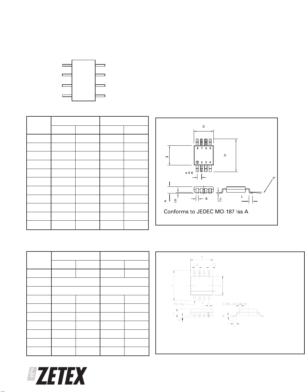
CONNECTION DIAGRAMS
EM
BAS
RE
V
CC
1
2
3
4
V
8
7
6
5
DRIVE
G
ND
FB
I
SENSE
MSOP8
DIM Millimetres Inches
MIN MAX MIN MAX
A 0.91 1.11 0.036 0.044
A1 0.10 0.20 0.004 0.008
B 0.25 0.36 0.010 0.014
C 0.13 0.18 0.005 0.007
D 2.95 3.05 0.116 0.120
e 0.65 NOM 0.0256 NOM
e1 0.33 NOM 0.0128 NOM
E 2.95 3.05 0.116 0.120
H 4.78 5.03 0.188 0.198
L 0.41 0.66 0.016 0.026
θ°
0° 6° 0° 6°
SO8
DIM Millimetres Inches
Min Max Min Max
A 4.80 4.98 0.189 0.196
B 1.27 BSC 0.05 BSC
C 0.53 REF 0.02 REF
D 0.36 0.46 0.014 0.018
E 3.81 3.99 0.15 0.157
F 1.35 1.75 0.05 0.07
G 0.10 0.25 0.004 0.010
J 5.80 6.20 0.23 0.24
K0° 8° 0° 8°
L 0.41 1.27 0.016 0.050
ISSUE 1 - JANUARY 2001
18
Page 19

ZXSC100
ORDERING INFORMATION
DEVICE Package Partmarking
ZXSC100X8 MSOP8 ZXSC100
ZXSC100N8 SO8 ZXSC100
Zetex plc.
Fields New Road, Chadderton, Oldham, OL9-8NP, United Kingdom.
Telephone: (44)161 622 4422 (Sales), (44)161 622 4444 (General Enquiries)
Fax: (44)161 622 4420
Zetex GmbH Zetex Inc. Zetex (Asia) Ltd. These are supported by
Streitfeldstraße 19 47 Mall Drive, Unit 4 3701-04 Metroplaza, Tower 1 agents and distributors in
D-81673 München Commack NY 11725 Hing Fong Road, major countries world-wide
Germany USA Kwai Fong, Hong Kong © Zetex plc 2001
Telefon: (49) 89 45 49 49 0 Telephone: (631) 543-7100 Telephone:(852) 26100 611
Fax: (49) 89 45 49 49 49 Fax: (631) 864-7630 Fax: (852) 24250 494 www.zetex.com
This publication is issued to provide outline information only which (unless agreed by the Company in writing) may not be used, applied or
reproduced for any purpose or form part of any order or contract or be regarded as a representation relating to the products or services
concerned. The Company reserves the right to alter without notice the specification, design, price or conditions of supply of any product or
service.
ISSUE 1 - JANUARY 2001
20
 Loading...