

Page 1
FIBRE CHANNEL COAXIAL
C
CABLE DRIVER AND LOOP
RESILIENCY CIRCUIT
PRELIMINARY
SY10EL1189
FEATURES
■ 425ps propagation delay
■ 1.6V output swings
■ Single +5V operation
■ Internal 75KΩ input pull-down resistors
■ Available in 16-pin SOIC package
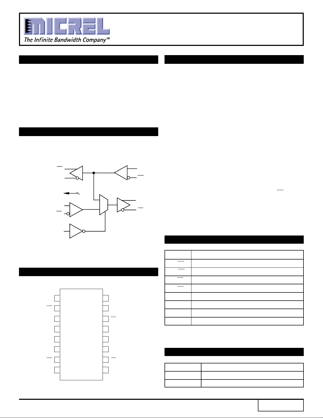
LOGIC DIAGRAM
From Input Cable
(ECL Levels)
Local
VBB
Local
SEL (TTL)
QR
QR
DT
DT
1
0
To Output Cable
(Enhanced Swing)
Receive Data
(ECL Levels)
Transmit Data
(ECL Levels)
DR
DR
QT
QT
DESCRIPTION
The SY10EL1189 is a differential receiver, differential
transmitter specifically designed to drive coaxial cables.
It incorporates the output cable driver capability of the
SY10EL89 Coaxial Cable Driver with additional circuitry
to multiplex the output cable drive source between the
cable receiver or the local transmitter inputs. The
multiplexer control circuitry is TTL compatible for ease of
operation.
The SY10EL1189 is useful as a bypass element for
Fibre Channel-Arbitrated Loop (FC-AL) or Serial Storage
Architecture (SSA) applications, to create loop style
interconnects with fault tolerant, active switches at each
device node. This device is particularly useful for back
panel applications where small size is desirable.
The EL89 style drive circuitry produces swings twice
as large as a standard PECL output. When driving a
coaxial cable, proper termination is required at both ends
of the line to minimize reflections. The 1.6V output swings
allow for proper termination at both ends of the cable.
Because of the larger output swings, the QT, QT outputs
are terminated into the thevenin equivalent of 50Ω to
VCC-3.0V instead of 50Ω to VCC-2.0V.
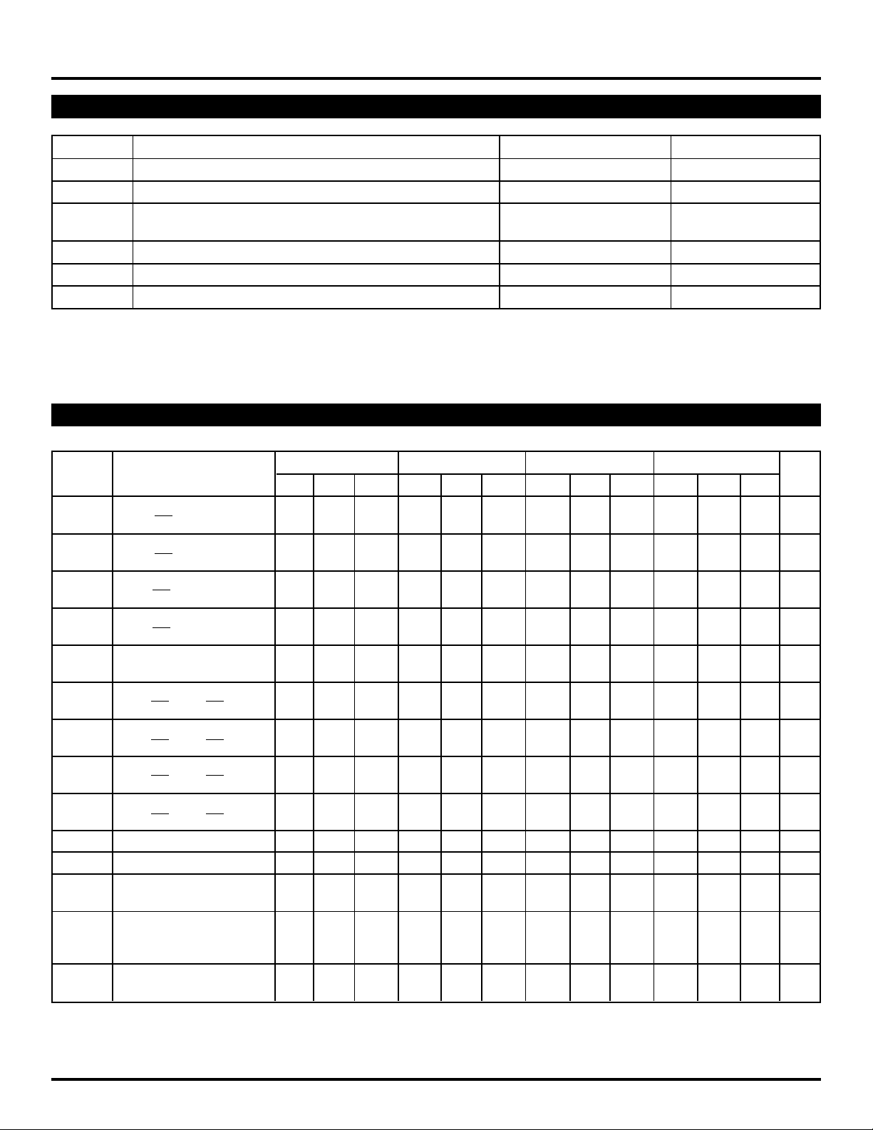
PIN NAMES
Pin Function
DR/DR Differential Input from Receive Cable
PIN CONFIGURATION
QR/QR Buffered Differential Output from Receive Cable
DT/DT Differential Input to Transmit Cable
QT/QT Buffered Differential Output to Transmit Cable
QR
QR
1
2
16
V
CC
15
DR
SEL Multiplexer Control Signal (TTL)
VCC Postive Power Supply
GND Ground
3
CC
V
4
N
V
CC
QT
QT
CC
V
5
6
7
8
Top View
SOIC
14
DR
13
GND
12
BB
V
11
DT
10
DT
9
SEL
BB Reference Voltage Output
V
TRUTH TABLE
SEL Function
L DR ➝ QT
H DT ➝ QT
Rev.: C Amendment: /2
1
Issue Date: January 2000
Page 2
Micrel
PRELIMINARY
SY10EL1189
ABSOLUTE MAXIMUM RATINGS
(1)
Symbol Rating Value Unit
VCC Power Supply Voltage (Referenced to GND) 0 to +7.0 V
VIN Input Voltage (Referenced to GND) 0 to VCC V
OUT Output Current — Continuous 50 mA
I
— Surge 100
TA Operating Temperature Range –40 to +85 °C
Tstore Storage Temperature Range –50 to +150 °C
CC Operating Voltage Range
V
NOTES:
1. Permanent device damage may occur if ABSOLUTE MAXIMUM RATINGS are exceeded. This is a stress rating only and functional operation is not implied
at conditions other than those detailed in the operational sections of this data sheet. Exposure to ABSOLUTE MAXIMUM RATlNG conditions for extended
periods may affect device reliability.
2. Parametric values specified at 4.75 to 5.25V.
DC ELECTRICAL CHARACTERISTICS
(2)
4.5 to 5.5 V
(1)
VCC = 5.0V, GND = 0V
A = –40°CTA = 0°CTA = +25°CTA = +85°C
T
Symbol Parameter Min. Typ. Max. Min. Typ. Max. Min. Typ. Max. Min. Typ. Max. Unit
OL Output LOW Voltage
V
(QR, QR)
V
OH Output HIGH Voltage
(QR, QR)
VOL Output LOW Voltage
(QT, QT)
V
OH Output HIGH Voltage
(QT, QT)
I
CC Quiescent Supply 20 25 42 22 26 47 23 27 47 25 28 47 mA
Current
(5)
VIL Input LOW Voltage
(DR,DR & DT,DT)
V
IH Input HIGH Voltage
(DR,DR & DT,DT)
I
IL Input LOW Current — — 150 — — 150 — — 150 — — 150 µA
(DR,DR & DT,DT)
IIH Input HIGH Current 0.5 — — 0.5 — — 0.5 — — 0.5 — — µA
(DR,DR & DT,DT)
VIL Input LOW Voltage SEL — — 0.8 — — 0.8 — — 0.8 — — 0.8 V
VIH Input HIGH Voltage SEL 2.0 — — 2.0 — — 2.0 — — 2.0 — — V
IIL Input LOW Current SEL
IH Input HIGH Current SEL
I
V
BB Output Reference 3.57 3.63 3.70 3.62 3.67 3.73 3.65 3.70 3.75 3.69 3.75 3.81 V
NOTES:
1. 10EL circuits are designed to meet the DC specifications shown in the
table after thermal equilibrium has been established. The circuit is
mounted in a test socket or mounted on a printed circuit board and
transverse air greater than 500lfm is maintained.
Voltage
(2)
(2,3)
(2,3)
(2)
(2)
3.05 3.23 3.35 3.05 3.24 3.37 3.05 3.24 3.37 3.05 3.25 3.41 V
3.92 4.05 4.11 3.98 4.09 4.16 4.02 4.11 4.19 4.09 4.16 4.28 V
(2,4)
1.94 2.22 2.50 1.83 2.12 2.41 1.80 2.10 2.39 1.77 2.06 2.35 V
(2,4)
3.71 3.89 4.08 3.79 3.98 4.17 3.83 4.02 4.20 3.90 4.09 4.28 V
3.05 — 3.50 3.05 — 3.52 3.05 — 3.52 3.05 — 3.56 V
3.77 — 4.11 3.83 — 4.16 3.87 — 4.19 3.94 — 4.28 V
VIN = 500mV — — 600 — — 600 — — 600 — — 600 µA
VIN = 2.7V — — 20 — — 20 — — 20 — — 20 µA
VIN = VCC — — 100 — — 100 — — 100 — — 100
2. Values will track 1:1 with the VCC supply.
3. Outputs loaded with 50Ω to +3.0V.
4. Outputs loaded with 50Ω to +2.0V.
5. Outputs open circuited.
2
Page 3

Micrel
PRELIMINARY
SY10EL1189
AC ELECTRICAL CHARACTERISTICS
(1)
VCC = 4.75 to 5.25V
A =–40°CTA = 0°C to 85˚C
T
Symbol Parameter Min. Typ. Max. Min. Typ. Max. Unit Condition
PLH Propagation Delay DR ➝ QR (Diff) 175 300 450 225 325 500 ps Note 2
t
tPHL to Output (SE) 150 300 500 175 325 550 Note 3
DR ➝ QT (Diff) 250 425 650 300 450 650
(SE) 225 425 700 250 450 700
DT ➝ QT (Diff) 225 400 650 275 425 650
(SE) 200 400 725 225 425 725
PLH Propagation Delay SEL ➝ QT, QT 450 600 850 500 650 800 ps 1.5V to 50% Pt
t
tPHL
tr Rise/Fall Time QR, QR 100 275 400 125 275 400 ps
tf (20% to 80%)
tr Rise/Fall Time QT, QT 150 300 550 150 300 550 ps
tf (20% to 80%)
tskew Within Device Skew
VPP Minimum Input Swing
CMR Common Mode Range
V
NOTES:
1. 10EL circuits are designed to meet the DC specifications shown in the table after thermal equilibrium has been established. The circuit is mounted in a
test socket or mounted on a printed circuit board and transverse air greater than 500lfm is maintained.
2. The differential propagation delay is defined as the delay from the crossing points of the differential input signals to the crossing point of the differential
output signals.
3. The single-ended propagation delay is defined as the delay from the 50% point of the input signal to the 50% point of the output signal.
4. Duty cycle skew is the difference between tPLH and tPHL propagation delay through a device.
5. Minimum input swing for which AC parameters are guaranteed.
6. The CMR range is referenced to the most positive side of the differential input signal. Normal operation is obtained if the HIGH level falls within the specified
range and the peak-to-peak voltage lies between VPP Min. and 1.0V.
(4)
(5)
(6)
—15 — — 15 —ps
200 — — 200 — — mV
3.00 — 4.35 3.00 — 4.35 V
PRODUCT ORDERING CODE
Ordering Package Operating
Code Type Range
SY10EL1189ZC Z16-2 Commercial
SY10EL1189ZCTR Z16-2 Commercial
3
Page 4

Micrel
16 LEAD SOIC .150" WIDE (Z16-2)
PRELIMINARY
SY10EL1189
Rev. 02
MICREL-SYNERGY 3250 SCOTT BOULEVARD SANTA CLARA CA 95054 USA
TEL + 1 (408) 980-9191 FAX + 1 (408) 914-7878 WEB http://www.micrel.com
This information is believed to be accurate and reliable, however no responsibility is assumed by Micrel for its use nor for any infringement of patents or
other rights of third parties resulting from its use. No license is granted by implication or otherwise under any patent or patent right of Micrel Inc.
© 2000 Micrel Incorporated
4
 Loading...