

Page 1
SCAN18245T
Non-Inverting Transceiver with TRI-STATE
®
Outputs
General Description
The SCAN18245T is a high speed, low-power bidirectional
line driver featuring separate data inputs organized into dual
9-bit bytes with byte-oriented output enable and direction
control signals. This device is compliant with IEEE 1149.1
Standard TestAccess Port and Boundary Scan Architecture
with the incorporation of the defined boundary-scan test
logic and test access port consisting of TestData Input (TDI),
Test Data Out (TDO), Test Mode Select (TMS), and Test
Clock (TCK).
Features
n IEEE 1149.1 (JTAG) Compliant
n Dual output enable control signals
n TRI-STATE outputs for bus-oriented applications
n 9-bit data busses for parity applications
n Reduced-swing outputs source 24 mA/sink 48 mA
n Guaranteed to drive 50Ω transmission line to TTL input
levels of 0.8V and 2.0V
n TTL compatible inputs
n 25 mil pitch Cerpack package
n Includes CLAMP and HIGHZ instructions
n Available as Known Good Die
n Standard Microcircuit Drawing (SMD) 5962-9311501
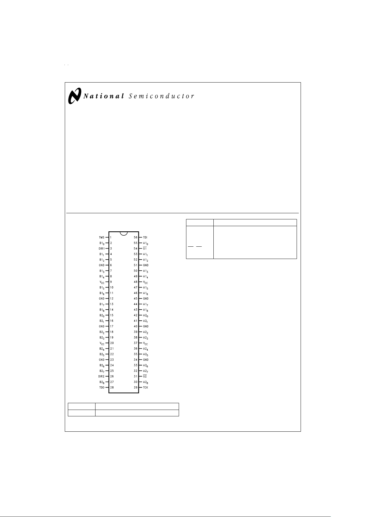
Connection Diagram
Pin Names Description
A1
(0–8)
Side A1 Inputs or TRI-STATE Outputs
Pin Names Description
B1
(0–8)
Side B1 Inputs or TRI-STATE Outputs
A2
(0–8)
Side A2 Inputs or TRI-STATE Outputs
B2
(0–8)
Side B2 Inputs or TRI-STATE Outputs
G1, G2
Output Enable Pins
DIR1, DIR2 Direction of Data Flow Pins
TRI-STATE®is a registered trademark of National Semiconductor Corporation.
DS100320-1
September 1998
SCAN18245T Non-Inverting Transceiver with TRI-STATE Outputs
© 1998 National Semiconductor Corporation DS100320 www.national.com
Page 2
Truth Tables
Inputs
A1
(0–8)B1(0–8)
G1
DIR1
LL H
←
H
LL L
←
L
LH H
→
H
LH L
→
L
HX Z Z
Inputs
A2
(0–8)B2(0–8)
G2
DIR2
LL H
←
H
LL L
←
L
LH H
→
H
LH L
→
L
HX Z Z
H=HIGH Voltage Level
L=LOW Voltage Level
X=Immaterial
Z=High Impedance
Functional Description
The SCAN18245 consists of two sets of nine non-inverting
bidirectional buffers with TRI-STATEoutputs and is intended
for bus-oriented applications. Direction pins (DIR1 and DIR2)
LOW enables data from B ports to A ports, when HIGH en-
ables data from A ports to B ports. The Output Enable pins
(G1 and G2) when HIGH disables both A and B ports by
placing them in a high impedance condition.
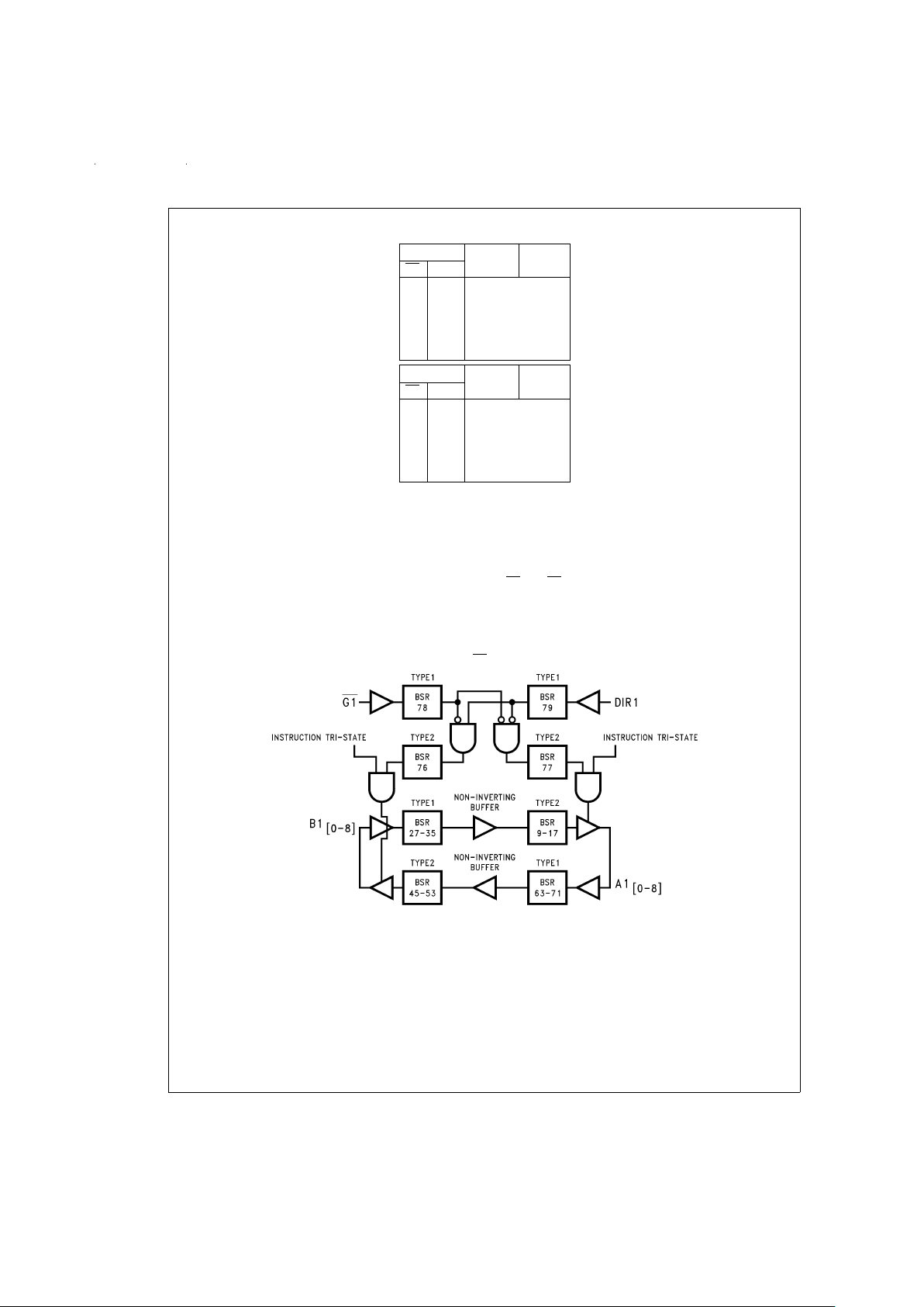
Block Diagrams
A1, B1, G1 and DIR1
DS100320-2
Note: BSR stands for Boundary Scan Register.
www.national.com 2
Page 3
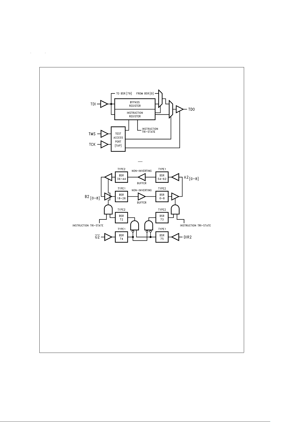
Block Diagrams (Continued)
Tap Controller
DS100320-3
A2, B2, G2 and DIR2
DS100320-4
Note: BSR stands for Boundary Scan Register.
www.national.com3
Page 4
Description of Boundary-Scan Circuitry
The scan cells used in the BOUNDARY-SCAN register are
one of the following two types depending upon their location.
Scan cell TYPE1 is intended to solely observe system data,
while TYPE2 has the additional ability to control system
data. (See IEEE Standard 1149.1
Figure 10–11
for a further
description of scan cell TYPE1 and
Figure 10–12
for a fur-
ther description of scan cell TYPE2.)
Scan cell TYPE1 is located on each system input pin while
scan cell TYPE2 is located at each system output pin as well
as at each of the two internal active-high output enable signals. AOE controls the activity of the A-outputs while BOE
controls the activity of the B-outputs. Each will activate their
respective outputs by loading a logic high.
The BYPASSregister is a single bit shift register stage identical to scan cell TYPE1. It captures a fixed logic low.
The INSTRUCTION register is an eight-bit register which
captures the value 00111101.
The two least significant bits of this captured value (01) are
required by IEEE Std 1149.1. The upper six bits are unique
to the SCAN18245T device. SCAN CMOS TestAccessLogic
devices do not include the IEEE 1149.1 optional identification register. Therefore, this unique captured value can be
used as a “pseudo ID” code to confirm that the correct device
is placed in the appropriate location in the boundary scan
chain.
MSB→LSB
Instruction Code Instruction
00000000 EXTEST
10000001 SAMPLE/PRELOAD
10000010 CLAMP
00000011 HIGHZ
All Others BYPASS
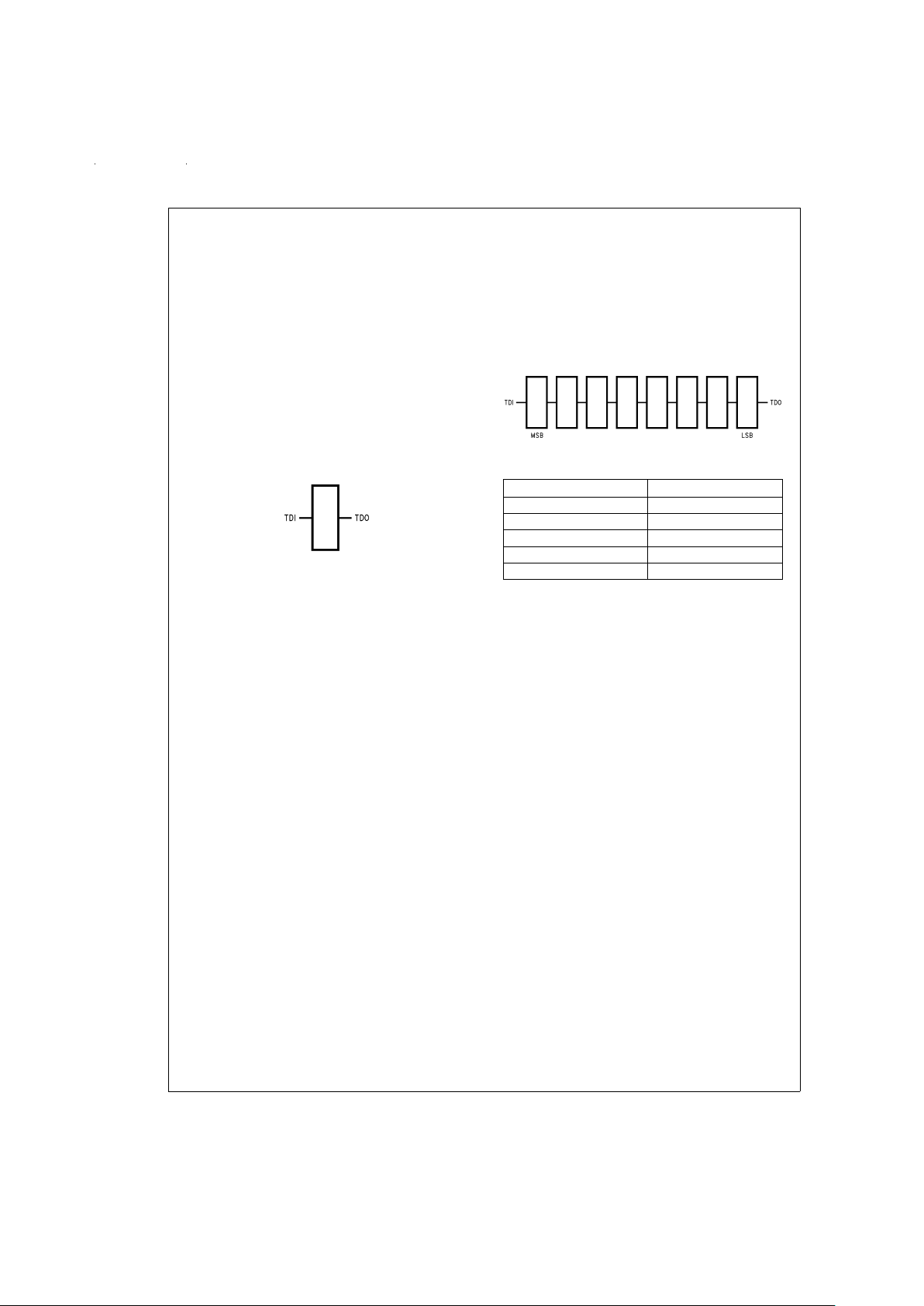
Bypass Register Scan Chain Definition
Logic 0
DS100320-9
Instruction Register Scan Chain Definition
DS100320-10
www.national.com 4
Page 5
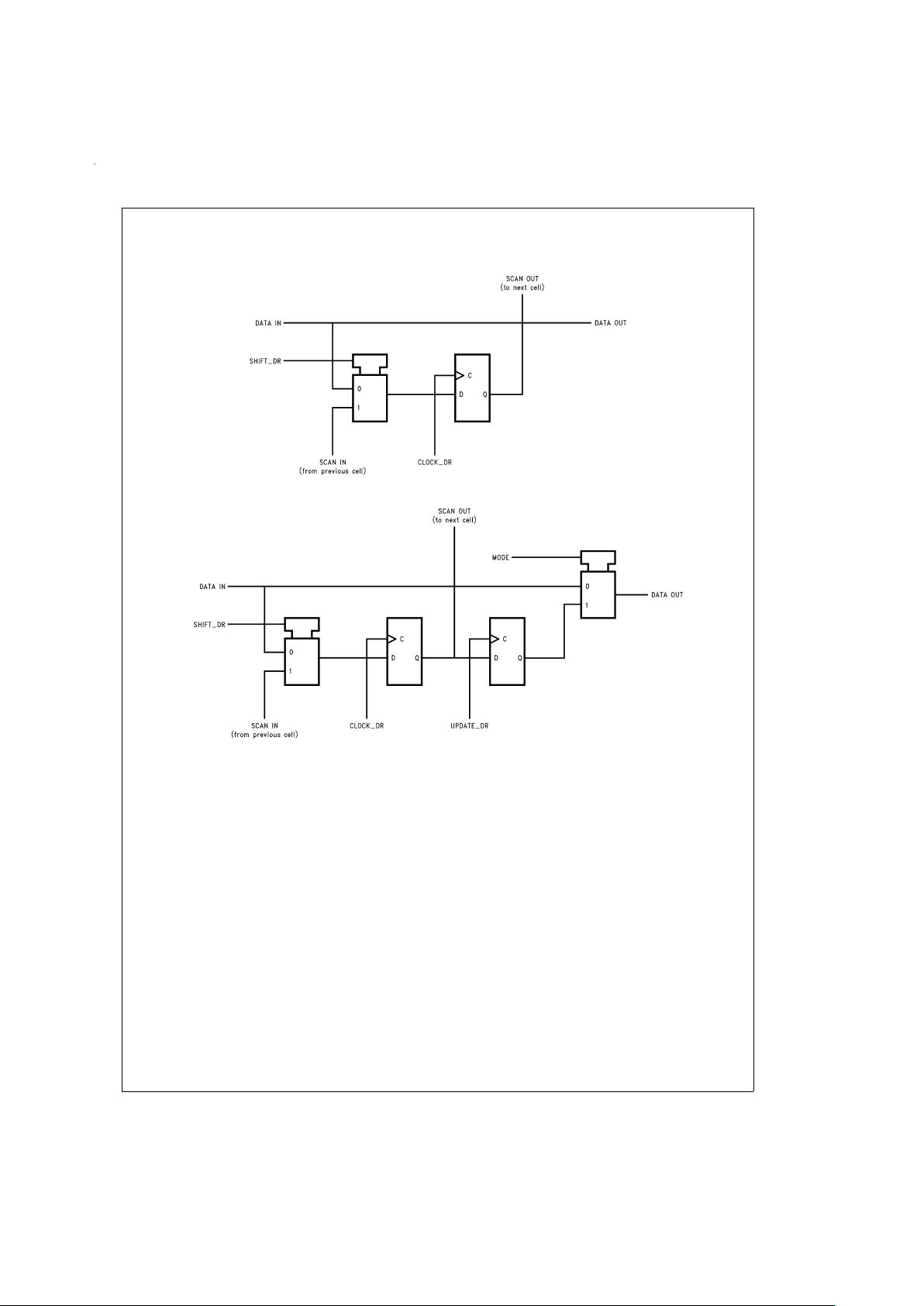
Description of Boundary-Scan Circuitry (Continued)
Scan Cell TYPE1
DS100320-7
Scan Cell TYPE2
DS100320-8
www.national.com5
Page 6

Description of Boundary-Scan Circuitry (Continued)
Boundary-Scan Register
Scan Chain Definition (80 Bits in Length)
DS100320-25
www.national.com 6
Page 7

Description of Boundary-Scan Circuitry (Continued)
Boundary-Scan Register Definition Index
Bit No. Pin Name Pin No. Pin Type Scan Cell Type
79 DIR1 3 Input TYPE1
Control
Signals
78 G1
54 Input TYPE1
77 AOE
1
Internal TYPE2
76 BOE
1
Internal TYPE2
75 DIR2 26 Input TYPE1
74 G2
31 Input TYPE1
73 AOE
2
Internal TYPE2
72 BOE
2
Internal TYPE2
71 A1
0
55 Input TYPE1
A1–in
70 A1
1
53 Input TYPE1
69 A1
2
52 Input TYPE1
68 A1
3
50 Input TYPE1
67 A1
4
49 Input TYPE1
66 A1
5
47 Input TYPE1
65 A1
6
46 Input TYPE1
64 A1
7
44 Input TYPE1
63 A1
8
43 Input TYPE1
62 A2
0
42 Input TYPE1
A2–in
61 A2
1
41 Input TYPE1
60 A2
2
39 Input TYPE1
59 A2
3
38 Input TYPE1
58 A2
4
36 Input TYPE1
57 A2
5
35 Input TYPE1
56 A2
6
33 Input TYPE1
55 A2
7
32 Input TYPE1
54 A2
8
30 Input TYPE1
53 B1
0
2 Output TYPE2
B1–out
52 B1
1
4 Output TYPE2
51 B1
2
5 Output TYPE2
50 B1
3
7 Output TYPE2
49 B1
4
8 Output TYPE2
48 B1
5
10 Output TYPE2
47 B1
6
11 Output TYPE2
46 B1
7
13 Output TYPE2
45 B1
8
14 Output TYPE2
44 B2
0
15 Output TYPE2
B2–out
43 B2
1
16 Output TYPE2
42 B2
2
18 Output TYPE2
41 B2
3
19 Output TYPE2
40 B2
4
21 Output TYPE2
39 B2
5
22 Output TYPE2
38 B2
6
24 Output TYPE2
37 B2
7
25 Output TYPE2
36 B2
8
27 Output TYPE2
www.national.com7
Page 8

Description of Boundary-Scan Circuitry (Continued)
Boundary-Scan Register Definition Index (Continued)
Bit No. Pin Name Pin No. Pin Type Scan Cell Type
35 B1
0
2 Input TYPE1
B1–in
34 B1
1
4 Input TYPE1
33 B1
2
5 Input TYPE1
32 B1
3
7 Input TYPE1
31 B1
4
8 Input TYPE1
30 B1
5
10 Input TYPE1
29 B1
6
11 Input TYPE1
28 B1
7
13 Input TYPE1
27 B1
8
14 Input TYPE1
26 B2
0
15 Input TYPE1
B2–in
25 B2
1
16 Input TYPE1
24 B2
2
18 Input TYPE1
23 B2
3
19 Input TYPE1
22 B2
4
21 Input TYPE1
21 B2
5
22 Input TYPE1
20 B2
6
24 Input TYPE1
19 B2
7
25 Input TYPE1
18 B2
8
27 Input TYPE1
17 A1
0
55 Output TYPE2
A1–out
16 A1
1
53 Output TYPE2
15 A1
2
52 Output TYPE2
14 A1
3
50 Output TYPE2
13 A1
4
49 Output TYPE2
12 A1
5
47 Output TYPE2
11 A1
6
46 Output TYPE2
10 A1
7
44 Output TYPE2
9A1
8
43 Output TYPE2
8A2
0
42 Output TYPE2
A2–out
7A2
1
41 Output TYPE2
6A2
2
39 Output TYPE2
5A2
3
38 Output TYPE2
4A2
4
36 Output TYPE2
3A2
5
35 Output TYPE2
2A2
6
33 Output TYPE2
1A2
7
32 Output TYPE2
0A2
8
30 Output TYPE2
www.national.com 8
Page 9

Absolute Maximum Ratings (Note 1)
If Military/Aerospace specified devices are required,
please contact the National Semiconductor Sales Office/
Distributors for availability and specifications.
Supply Voltage (V
CC
) −0.5V to +7.0V
DC Input Diode Current (I
IK
)
V
I
=
−0.5V −20 mA
V
I
=
V
CC
+0.5V +20 mA
DC Output Diode Current (I
OK
)
V
O
=
−0.5V −20 mA
V
O
=
V
CC
+0.5V +20 mA
DC Output Voltage (V
O
) −0.5V to VCC+0.5V
DC Output Source/Sink Current (I
O
)
±
70 mA
DC V
CC
or Ground Current
Per Output Pin
±
70 mA
Junction Temperature
Cerpack +175˚C
Storage Temperature −65˚C to +150˚C
ESD (Min) 2000V
Recommended Operating
Conditions
Supply Voltage (VCC)
SCAN Products 4.5V to 5.5V
Input Voltage (V
I
) 0VtoV
CC
Output Voltage (VO) 0VtoV
CC
Operating Temperature (TA)
Military −55˚C to +125˚C
Minimum Input Edge Rate dV/dt 125 mV/ns
V
IN
from 0.8V to 2.0V
V
CC
@
4.5V, 5.5V
Note 1: Absolute maximum ratings are those values beyond which damage
to the device may occur. The databook specifications should be met, without
exception, to ensure that the system design is reliable over its power supply,
temperature, and output/input loading variables. National does not recommend operation of SCAN circuits outside databook specifications.
DC Electrical Characteristics
Symbol Parameter V
CC
(V)
Military Units Conditions
T
A
=
−55˚C to +125˚C
Guaranteed Limits
V
IH
Minimum High 4.5 2.0 V V
OUT
=
0.1V
Input Voltage 5.5 2.0 or V
CC
−0.1V
V
IL
Maximum Low 4.5 0.8 V V
OUT
=
0.1V
Input Voltage 5.5 0.8 or V
CC
−0.1V
V
OH
Minimum High 4.5 3.15 V I
OUT
=
−50 µA
Output Voltage 5.5 4.15
4.5 2.4 V V
IN
=
V
IL
or V
IH
5.5 2.4 I
OH
=
−24 mA
V
OL
Maximum Low 4.5 0.1 V I
OUT
=
50 µA
Output Voltage 5.5 0.1
4.5 0.55 V V
IN
=
V
IL
or V
IH
5.5 0.55 I
OL
=
48 mA
I
IN
Maximum Input 5.5
±
1.0 µA V
I
=
V
CC
, GND
Leakage Current
I
IN
Maximum Input 5.5 3.7 µA V
I
=
V
CC
TDI, TMS Leakage −385 µA V
I
=
GND
Minimum Input 5.5 −160 µA V
I
=
GND
Leakage
I
OLD
Minimum Dynamic 5.5 63 mA V
OLD
=
0.8V Max
I
OHD
Output Current
(Note 3)
−27 mA V
OHD
=
2.0V Min
I
OZT
Maximum I/O VI(OE)=VIL,V
IH
Leakage Current 5.5
±
11.0 µA V
I
=
V
CC
, GND
V
O
=
V
CC
, GND
I
OS
Output Short 5.5 −100 mA (min) V
O
=
0V
Circuit Current
I
CC
Maximum Quiescent 5.5 168 µA V
O
=
High
Supply Current TDI, TMS=V
CC
5.5 930 µA V
O
=
High
TDI, TMS=GND
www.national.com9
Page 10
DC Electrical Characteristics (Continued)
Symbol Parameter V
CC
(V)
Military Units Conditions
T
A
=
−55˚C to +125˚C
Guaranteed Limits
I
CCt
Maximum ICCPer
Input
5.5 2.0 mA V
I
=
V
CC
–2.1V
V
I
=
V
CC
–2.1V
5.5 2.15 mA TDI/TMS Pin, test
one with the
other floating
Note 2: All outputs loaded; thresholds associated with output under test.
Note 3: Maximum test duration 2.0 ms, one output loaded at a time.
Noise Specifications
Symbol Parameter V
CC
(V)
Military Units
T
A
=
−55˚C to +125˚C
Guaranteed Limits
V
OLP
Maximum High 5.0 0.8 V
Output Noise (Notes 4, 5)
V
OLV
Minimum Low 5.0 -0.8 V
Output Noise (Notes 4, 5)
Note 4: Maximum number of outputs that can switch simultaneously is n. (n-1) outputs are switched LOW and one output held LOW.
Note 5: Maximum number of outputs that can switch simultaneously is n. (n-1) outputs are switched HIGH and one output held HIGH.
AC Electrical Characteristics
Normal Operation
Symbol Parameter V
CC
(V)
(Note 7)
Military Units
T
A
=
−55˚C to +125˚C
C
L
=
50 pF
Min Max
t
PLH
, Propagation Delay 5.0 1.6 10.0 ns
t
PHL
A to B, B to A 1.6 11.0
t
PLZ
, Disable Time 5.0 1.2 10.0 ns
t
PHZ
1.2 9.5
t
PZL
, Enable Time 5.0 1.6 13.0 ns
t
PZH
1.6 11.0
www.national.com 10
Page 11

AC Electrical Characteristics
Scan Test Operation
Symbol Parameter V
CC
(V)
(Note 7)
Military Units
T
A
=
−55˚C to +125˚C
C
L
=
50 pF
Min Max
t
PLH
, Propagation Delay 5.0 2.8 15.8 ns
t
PHL
TCK to TDO 2.8 15.8
t
PLZ
, Disable Time 5.0 2.0 12.8 ns
t
PHZ
TCK to TDO 2.0 12.8
t
PZL
, Enable Time 5.0 2.4 16.7 ns
t
PZH
TCK to TDO 2.4 16.7
t
PLH
, Propagation Delay 5.0 4.0 21.7 ns
t
PHL
TCK to Data Out 4.0 21.7
During Update-DR
State
t
PLH
, Propagation Delay 4.0 21.2 ns
t
PHL
TCK to Data Out 5.0 4.0 21.2
During Update-IR
State
t
PLH
, Propagation Delay 5.0 4.4 23.0 ns
t
PHL
TCK to Data Out 4.4 23.0
During Test Logic
Reset State
t
PLZ
, Propagation Delay 5.0 3.2 19.6 ns
t
PHZ
TCK to Data Out 3.2 19.6
During Update-DR
State
t
PLZ
, Propagation Delay 5.0 2.8 20.9 ns
t
PHZ
TCK to Data Out 2.8 20.9
During Update-IR
State
t
PLZ
, Propagation Delay 5.0 2.8 21.8 ns
t
PHZ
TCK to Data Out 2.8 21.8
During Test Logic
Reset State
t
PZL
, Propagation Delay 5.0 4.0 22.6 ns
t
PZH
TCK to Data Out 4.0 22.6
During Update-DR
State
t
PZL
, Propagation Delay 5.0 3.2 23.7 ns
t
PZH
TCK to Data Out 3.2 23.7
During Update-IR
State
t
PZL
, Propagation Delay 5.0 3.6 24.9 ns
t
PZH
TCK to Data Out 3.6 24.9
During Test Logic
Reset State
Note 6: All Propagation Delays involving TCK are measured from the falling edge of TCK.
www.national.com11
Page 12

AC Operating Requirements
Scan Test Operation
Symbol Parameter V
CC
(V)
(Note 7)
Military Units
T
A
=
−55˚C to +125˚C
C
L
=
50 pF
Guaranteed Minimum
t
S
Setup Time, H or L 5.0 0.0 ns
Data to TCK (Note 8)
t
H
Hold Time, H or L 5.0 6.5 ns
TCK to Data (Note 8)
t
S
Setup Time, H or L 5.0 0.0 ns
G1 , G2 to TCK (Note 9)
t
H
Hold Time, H or L 5.0 4.0 ns
TCK to G1, G2 (Note 9)
t
S
Setup Time, H or L 5.0 0.0 ns
DIR1, DIR2 to TCK
(Note 11)
t
H
Hold Time, H or L 5.0 4.0 ns
TCK to DIR1, DIR2
(Note 11)
t
S
Setup Time, H or L
Internal AOE
n
, BOE
n
5.0 1.0 ns
to TCK (Note 10)
t
H
Hold Time, H or L 5.0 4.0 ns
TCK to Internal AOE
n
,
BOE
n
(Note 10)
t
S
Setup Time, H or L 5.0 7.0 ns
TMS to TCK
t
H
Hold Time, H or L 5.0 2.0 ns
TCK to TMS
t
S
Setup Time, H or L 5.0 1.0 ns
TDI to TCK
t
H
Hold Time, H or L 5.0 3.5 ns
TCK to TDI
t
W
Pulse Width 5.0
H 12.0 ns
L 5.0
f
max
Maximum TCK 5.0 25 MHz
Clock Frequency
T
PU
Wait Time, 5.0 100 ns
Power Up to TCK
T
DN
Power Down 0.0 100 ms
Delay
Note 7: Voltage Range 5.0 is 5.0V±0.5V.
All Input Timing Delays involving TCK are measured from the rising edge of TCK.
Note 8: Timing pertains to the TYPE1 BSR and TYPE2 BSR after the buffer (BSR 0–8, 9–17, 18–26, 27–35, 36–44, 45–53, 54–62, 63–71).
Note 9: Timing pertains to BSR 74 and 78 only.
Note 10: Timing pertains to BSR 72, 73, 76 and 77 only.
Note 11: Timing pertains to BSR 75 and 79 only.
www.national.com 12
Page 13

Capacitance
Symbol Parameter Typ Units Conditions
C
IN
Input Pin Capacitance 4 pF V
CC
=
5.0V
C
I/O
Input/Output Capacitance 20 pF V
CC
=
5.0V
C
PD
Power Dissipation 41 pF V
CC
=
5.0V
Capacitance
Pad Diagram
DS100320-24
www.national.com13
Page 14

SCAN18245T Die Information
Die Revision Z
Die ID Y8J245
Die Size (X) 4310 µm
Die Size (Y) 4310 µm
Die Thickness 14 mil
Substrate Bias V
CC
(optional)
Backside Coating None
Pad Locations
Signal Signal Pad Location
Number Name (Note 12)
1 TMS −8.58, 77.81
2B1
0
−19.94, 77.81
3 DIR1 −30.50, 77.81
4B1
1
−40.98, 77.81
5B1
2
−53.59, 77.81
6 GND −63.73, 77.81
7B1
3
−74.47, 77.81
8B1
4
−79.73, 62.30
9V
CC
−79.73, 51.55
−79.73, 46.28
10 B1
5
−79.73, 36.05
11 B1
6
−79.73, 27.48
12 GND −79.72, 19.46
13 B1
7
−79.73, 10.09
14 B1
8
−79.73, 3.46
15 B2
0
−79.73, −3.43
16 B2
1
−79.73, −10.06
17 GND −79.72, −19.43
18 B2
2
−79.73, −27.45
19 B2
3
−79.73, −36.02
20 V
CC
−79.73, −46.24
−79.73, −51.52
21 B2
4
−79.73, −62.27
22 B2
5
−74.47, −77.81
23 GND −63.73, −77.81
24 B2
6
−53.59, −77.81
25 B2
7
−40.98, −77.81
26 DIR2 −30.50, −77.81
27 B2
8
−19.94, −77.81
28 TDO −8.58, −77.81
29 TCK 5.54, −77.81
30 A2
8
19.94, −77.81
31 G2
30.50, −77.81
32 A2
7
40.98, −77.81
33 A2
6
53.59, −77.81
34 GND 63.73, −77.81
35 A2
5
74.47, −77.81
36 A2
4
79.73, −62.27
www.national.com 14
Page 15

Pad Locations (Continued)
Signal Signal Pad Location
Number Name (Note 12)
37 V
CC
79.73, −51.50
79.73, −46.23
38 A2
3
79.73, −36.02
39 A2
2
79.73, −27.40
40 GND 79.73, −19.43
41 A2
1
79.73, −10.06
42 A2
0
79.73, −3.43
43 A1
8
79.73, 3.46
44 A1
7
79.73, 10.09
45 GND 79.72, 19.46
46 A1
6
79.73, 27.43
47 A1
5
79.73, 36.05
48 V
CC
79.73, 46.26
79.73, 51.54
49 A1
4
79.73, 62.30
50 A1
3
74.47, 77.81
51 GND 63.73, 77.81
52 A1
2
53.59, 77.81
53 A1
1
40.98, 77.81
54 G1
30.50, 77.81
55 A1
0
19.94, 77.81
56 TDI 5.54, 77.81
Note 12: X, Y coordinates measured in mils from center of die.
www.national.com15
Page 16

Physical Dimensions inches (millimeters) unless otherwise noted
LIFE SUPPORT POLICY
NATIONAL’S PRODUCTS ARE NOT AUTHORIZED FOR USE AS CRITICAL COMPONENTS IN LIFE SUPPORT DEVICES OR SYSTEMS WITHOUT THE EXPRESS WRITTEN APPROVAL OF THE PRESIDENT OF NATIONAL SEMICONDUCTOR CORPORATION. As used herein:
1. Life support devices or systems are devices or systems which, (a) are intended for surgical implant into
the body, or (b) support or sustain life, and whose failure to perform when properly used in accordance
with instructions for use provided in the labeling, can
be reasonably expected to result in a significant injury
to the user.
2. A critical component in any component of a life support
device or system whose failure to perform can be reasonably expected to cause the failure of the life support
device or system, or to affect its safety or effectiveness.
National Semiconductor
Corporation
Americas
Tel: 1-800-272-9959
Fax: 1-800-737-7018
Email: support@nsc.com
www.national.com
National Semiconductor
Europe
Fax: +49 (0) 1 80-530 85 86
Email: europe.support@nsc.com
Deutsch Tel: +49 (0) 1 80-530 85 85
English Tel: +49 (0) 1 80-532 78 32
Français Tel: +49 (0) 1 80-532 93 58
Italiano Tel: +49 (0) 1 80-534 16 80
National Semiconductor
Asia Pacific Customer
Response Group
Tel: 65-2544466
Fax: 65-2504466
Email: sea.support@nsc.com
National Semiconductor
Japan Ltd.
Tel: 81-3-5620-6175
Fax: 81-3-5620-6179
56-Lead Ceramic Flatpak (F)
NS Package Number WA56A
SCAN18245T Non-Inverting Transceiver with TRI-STATE Outputs
National does not assume any responsibility for use of any circuitry described, no circuit patent licenses are implied and National reserves the right at any time without notice to change said circuitry and specifications.
 Loading...