

Datasheet KU80C51SL-AH, KU87C51SL-AH, KU83C51SL-AH, KU81C51SL-AH, SB80C51SL-AL Datasheet (Intel Corporation)
...Page 1
*Other brands and names are the property of their respective owners.
Information in this document is provided in connection with Intel products. Intel assumes no liability whatsoever, including infringement of any patent or
copyright, for sale and use of Intel products except as provided in Intel’s Terms and Conditions of Sale for such products. Intel retains the right to make
changes to these specifications at any time, without notice. Microcomputer Products may have minor variations to this specification known as errata.
November 1994COPYRIGHT©INTEL CORPORATION, 1995 Order Number: 272271-002
8XC51SL/LOW VOLTAGE 8XC51SL
KEYBOARD CONTROLLER
80C51SL Ð CPU with RAM and I/O; V
CC
e
5Vg10%
81C51SL Ð 16K ROM Preprogrammed with SystemSoft Keyboard Controller and Scanner
Firmware. V
CC
e
5Vg10%.
83C51SL Ð 16K Factory Programmed ROM. V
CC
e
5Vg10%.
87C51SL Ð 16K OTP ROM. V
CC
e
5Vg10%.
Low Voltage 80C51SLÐCPU with RAM and I/O; V
CC
e
3.3Vg0.3V
Low Voltage 81C51SLÐ 16K ROM Preprogrammed with SystemSoft Keyboard Controller
and Scanner Firmware. V
CC
e
3.3Vg0.3V.
Low Voltage 83C51SLÐ 16K Factory Programmed ROM. V
CC
e
3.3Vg0.3V.
Low Voltage 87C51SLÐ 16K OTP ROM. V
CC
e
3.3Vg0.3V.
Y
Proliferation of 8051 Architecture
Y
Complete 8042 Keyboard Control
Functionality
Y
8042 Style Host Interface
Y
Optional Hardware Speedup of
GATEA20 and RCL
Y
Local 16 x 8 Keyboard Switch Matrix
Support
Y
Two Industry Standard Serial Keyboard
Interfaces; Supported via Four High
Drive Outputs
Y
5 LED Drivers
Y
Low Power CHMOS Technology
Y
4-Channel, 8-Bit A/D
Y
Interface for up to 32 Kbytes of
External Memory
Y
Slew Rate Controlled I/O Buffers Used
to Minimize Noise
Y
256 Bytes Data RAM
Y
Three Multifunction I/O Ports
Y
10 Interrupt Sources with 6 UserDefinable External Interrupts
Y
2 MHz – 16 MHz Clock Frequency
Y
100-Pin PQFP (8XC51SL)
100-Pin SQFP (Low Voltage 8XC51SL)
The 8XC51SL, based on Intel’s industry-standard MCSÉ51 microcontroller family, is designed for keyboard
control in laptop and notebook PCs. The highly integrated keyboard controller incorporates an 8042-style UPI
host interface with expanded memory, keyboard scan, and power management. The 8XC51SL supports both
serial and scanned keyboard interfaces and is available in pre-programmed versions to reduce time to market.
The Low Voltage 8XC51SL is the 3.3V version optimized for even further power savings. Throughout the
remainder of this document, both devices will generally be referred to as 51SL.
The 8XC51SL is a pin-for-pin compatible replacement for the 8XC51SL-BG. It does, however have some
additional functionality. Those additional functions are as follows:
1. 16K OTP ROM: The 8XC51SL-BG had only 8K of ROM.
2. New Register Set: The 8XC51SL adds a second set of host interface registers available for use in supporting power management. This required an additional address line (A1) for decoding. To accommodate this,
one V
CC
pin was removed. However, in order to maintain compatibility with the -BG version, an enable bit
for this new register set was added in configuration register 1. This allows the 8XC51SL to be drop in
compatible to existing 8XC51SL-BG designs; no software modifications required.
NOTE:
The changes made to the V
CC
pins require that all three VCCpins be properly connected. Failing to do so
could result in high leakage current and possible damage to the device.
Page 2
8XC51SL/LOW VOLTAGE 8XC51SL
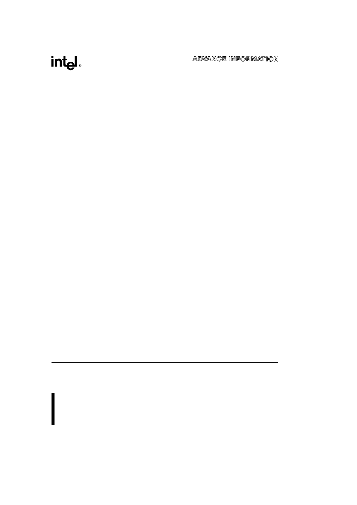
272271– 1
Figure 1. Block Diagram
2
Page 3
8XC51SL/LOW VOLTAGE 8XC51SL
272271– 2
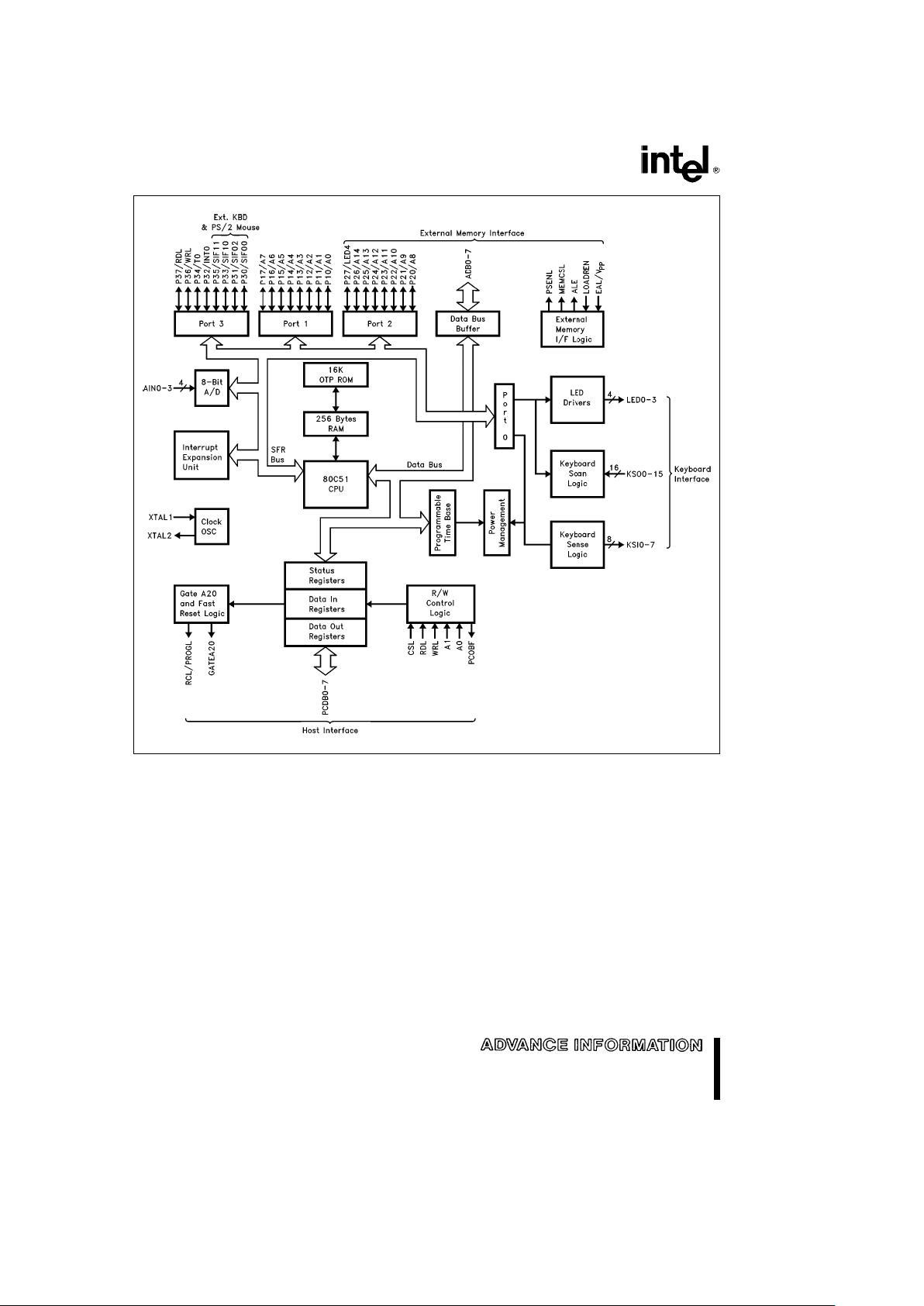
Figure 2. Connection Diagram (PQFP and SQFP)
PACKAGES
Part Prefix Suffix Package Type
8XC51SL KU AH 100-Pin PQFP
Low Voltage 8XC51SL SB AL 100-Pin SQFP
3
Page 4
8XC51SL/LOW VOLTAGE 8XC51SL
PIN DESCRIPTIONS
Table 1. Pin Descriptions
Symbol Type Description
V
SS
Circuit ground potential.
V
CC
Supply voltage during normal, Idle, and Power-Down operation; nominallya5V
g
10% for 8XC51SL,a3.3Vg0.3V for Low Voltage 8XC51SL.
PCDB0–7 I/O Host interface data bus. An 8-bit bidirectional port for data transfers between the
host processor and the keyboard controller.
WRL I The active-low, host-interface write signal.
RDL I The active-low, host-interface read signal.
CSL I The active-low, host-interface chip select.
A0–A1 I Host-Interface Address select inputs.
PCOBF O The active-high, host-interface Output Buffer Full interrupt.
GATEA20 O Gate A20 control signal output.
RCL/PROGL O Host resetÐactive low. This pin is also the program pulse input during EPROM
programming.
LED0–3 O LED output drivers.
KSI0–7 I Keyboard input scan lines (input Port 0). Schmitt inputs with 5K –20K pull-up
resistors.
KSO0–15 O Keyboard output scan lines.
PORT 1 I/O Port 1 is a general-purpose, 8-bit bidirectional port with internal pull-ups. It also
supports the following user-selectable functions:
P10/A0– P10–P16 are available for connection to dedicated keyboard inputs. A0 – A7 output
the low-order address byte (refer to LOADREN signal).
P17/A7
LOADREN I Low address enable. When set high, address bits A0 –A7 are output on P10–P17.
PORT2 I/O Port 2 is a general-purpose, 8-bit bidirectional port with internal pull-ups on P20 – 6/
A8–14. It also supports the following user-selectable functions:
P20–6/A8– 14 P20– 6/A8 – 14 output the high-order address byte.
P27/LED4 P27/LED4 is available as a fifth LED output driver (by writing to the port bit 7).
PORT 3 I/O Port 3 is a general-purpose, 8-bit bidirectional port. P32/INT0, P34/T0, P36/WRL,
and P37/RDL have internal pull-ups. P30/SIF00, P31/SIF01, P33/SIF10, and
P35/SIF11 are high-drive open-drain outputs. It also supports the following user-
selectable functions:
P30/SIF00 A high-drive, open-drain output to support an external serial keyboard interface
(typically CLK); RXD (8051 UART serial input port); SIF0INTL (serial interface
interrupt 0).
P31/SIF01 A high-drive, open-drain output to support an external serial keyboard interface
(typically DATA); TXD (8051 UART serial output port).
P32/INT0 INT0L (external interrupt 0).
P33/SIF10 A high-drive, open-drain output to support an external serial keyboard interface
(typically mouse CLK); SIF1INTL (external interrupt 1).
P34/T0 AUXOBF1 (output buffer fullÐmouse support); T0 (Timer/Counter 0 external
input).
P35/SIF11 A high-drive, open-drain output to support an external serial keyboard interface
(typically mouse DATA); T1 (Timer/Counter 1 external input).
P36/WRL WRL (external data memory write strobe); inactive at addresses 7FF0 – 7FFFH.
P37/RDL AUXOBF2 (output buffer full interrupt); INT2L (external interrupt); RDL (external
data memory read strobe); inactive at addresses 7FF0 – FFFFH.
4
Page 5
8XC51SL/LOW VOLTAGE 8XC51SL
PIN DESCRIPTIONS (Continued)
Table 1. Pin Descriptions (Continued)
Symbol Type Description
XTAL1 I Input to the on-chip oscillator.
XTAL2 O Output from the on-chip oscillator.
AVGND Analog ground potential.
AVREF Analog supply voltage; nominallya5Vg10% for 8XC51SL,a3.3Vg0.3V for Low
Voltage 8XC51SL.
AIN0–3 I A/D Analog input channels.
ADB0–7 I/O External address/data bus. Multiplexes the low-address byte and data during external
memory accesses.
EAL/V
PP
I External address input. When held high, the 51SL CPU executes out of internal Program
Memory unless the program counter exceeds 3FFFH. When held low, the 51SL CPU
always executes out of external memory. EAL is latched on the falling edge of RST. This
pin also receives the programming supply voltage (V
PP
) during EPROM programming.
ALE O Address Latch Enable output pulse latches the low address byte during external
memory access. ALE is output at a constant rate of (/6 the oscillator frequency, whether
or not there are accesses to external memory. One ALE pulse is skipped during the
execution of a MOVX instruction. ALE is disabled during Idle mode and can also be
disabled via Configuration register 1 control.
PSENL O Program Store Enable is the read strobe to external program memory. PSENL is
qualified with RDL and A15 for use with an external Flash memory. PSENL is not active
when the device executes out of internal program memory.
MEMCSL I/O External Memory Chip Select for code space address 4000H and above, when EAL is
inactive (i.e., high). For EAL low, MEMCSL is active. Goes inactive during Idle mode and
Power-Down mode. If external memory interfacing is not required, MEMCSL can be
configured as a general purpose I/O (controlled via Configuration register 1).
RST I Resets the keyboard controller. Hold RST high for two machine cycles.
5
Page 6
8XC51SL/LOW VOLTAGE 8XC51SL
8XC51SL/LOW VOLTAGE 8XC51SL PIN CHARACTERISTICS
Table 2. Pin Characteristics
Pin No. Pin Name Type Term Reset PD Mode
1 KSO0 O OD TRI HOLD
2 KSO1 O OD TRI HOLD
3 KSO2 O OD TRI HOLD
4 KSO3 O OD TRI HOLD
5 KSO4 O OD TRI HOLD
6 KSO5 O OD TRI HOLD
7 KSO6 O OD TRI HOLD
8 KSO7 O OD TRI HOLD
9 KSO8 O OD TRI HOLD
10 KSO9 O OD TRI HOLD
11 KSO10 O OD TRI HOLD
12 KSO11 O OD TRI HOLD
13 V
SS
14 V
CC
15 KSO12 O OD TRI HOLD
16 KSO13 O OD TRI HOLD
17 KSO14 O OD TRI HOLD
18 KSO15 O OD L HOLD
19 KSI0 I 5K–20K PU NC
20 KSI1 I 5K–20K PU NC
21 KSI2 I 5K–20K PU NC
22 KSI3 I 5K–20K PU NC
23 KSI4 I 5K–20K PU NC
24 KSI5 I 5K–20K PU NC
25 KSI6 I 5K–20K PU NC
26 KSI7 I 5K–20K PU NC
27 ALE O L L
28 MEMCSL O L (EALe0) H
29 PSENL O L L
30 P10/A0 I/O PU WH HOLD
31 P11/A1 I/O PU WH HOLD
32 P12/A2 I/O PU WH HOLD
33 P13/A3 I/O PU WH HOLD
34 P14/A4 I/O PU WH HOLD
35 P15/A5 I/O PU WH HOLD
36 P16/A6 I/O PU WH HOLD
37 P17/A7 I/O PU WH HOLD
6
Page 7
8XC51SL/LOW VOLTAGE 8XC51SL
8XC51SL/LOW VOLTAGE 8XC51SL PIN CHARACTERISTICS (Continued)
Table 2. Pin Characteristics (Continued)
Pin No. Pin Name Type Term Reset PD Mode
38 V
SS
39 V
SS
40 ADB0 I/O TRI TRI
41 ADB1 I/O TRI TRI
42 ADB2 I/O TRI TRI
43 ADB3 I/O TRI TRI
44 ADB4 I/O TRI TRI
45 ADB5 I/O TRI TRI
46 ADB6 I/O TRI TRI
47 ADB7 I/O TRI TRI
48 P20/A8 I/O PU WH HOLD
49 P21/A9 I/O PU WH HOLD
50 P22/A10 I/O PU WH HOLD
51 P23/A11 I/O PU WH HOLD
52 P24/A12 I/O PU WH HOLD
53 P25/A13 I/O PU WH HOLD
54 P26/A14 I/O PU WH HOLD
55 P27/LED4 I/O OD TRI HOLD
56 V
SS
57 GATEA20 O WH HOLD
58 PCDB7 I/O TRI TRI
59 PCDB6 I/O TRI TRI
60 PCDB5 I/O TRI TRI
61 PCDB4 I/O TRI TRI
62 PCDB3 I/O TRI TRI
63 PCDB2 I/O TRI TRI
64 RCL/PROGL O WH HOLD
65 V
CC
66 PCDB1 I/O TRI TRI
67 PCDB0 I/O TRI TRI
68 RST I
69 XTAL2 O H
70 XTAL1 I
71 PCOBF O L HOLD
72 CSL I
73 RDL I
74 WRL I
7
Page 8

8XC51SL/LOW VOLTAGE 8XC51SL
8XC51SL/LOW VOLTAGE 8XC51SL PIN CHARACTERISTICS (Continued)
Table 2. Pin Characteristics (Continued)
Pin No. Pin Name Type Term Reset PD Mode
75 A0 I
76 AIN3 I
77 AIN2 I
78 AIN1 I
79 AIN0 I
80 AVREF
81 AVGND
82 V
CC
83 V
SS
84 P37/RDL I/O PU WH HOLD
85 P36/WRL I/O PU WH HOLD
86 P35/SIF11 I/O OD TRI HOLD
87 P34/T0 I/O PU WH HOLD
88 P33/SIF10 I/O OD L HOLD
89 P32/INT0 I/O PU WH HOLD
90 P31/SIF01 I/O OD TRI HOLD
91 P30/SIF00 I/O OD L HOLD
92 A1 I
93 V
SS
94 EAL I
95 LOADREN I
96 V
SS
97 LED3 O OD TRI HOLD
98 LED2 O OD TRI HOLD
99 LED1 O OD TRI HOLD
100 LED0 O OD TRI HOLD
NOTES:
1. During Power Down mode all floating I/O pins or inputs without internal pullups should be driven.
2. PU
e
Pulled Up, ODeOpen Drain, WHeWeak High, TRIeTri-State.
8
Page 9

8XC51SL/LOW VOLTAGE 8XC51SL
PORT STRUCTURES AND
OPERATION
All three 51SL ports are bidirectional. Each consists
of a latch (Special Function Registers P1 through
P3), an output driver, and an input buffer. Port 0 of
the 51SL CPU does not connect to the package
pins. It is used internally to drive the keyboard scan
logic.
The output drivers of ports 1 and 2 can be used in
accesses to external memory. The 51SL provides
the LOADREN signal to facilitate external memory
interfaces. When the LOADREN signal is high, Port
1 outputs the low byte of the external memory address. If LOADREN is tied low, then the Port 1 signals continue to emit the P1 SFR content. Port 2
outputs the upper seven bits of the high byte of the
external address when the address is 15 bits wide
and either EAL is tied low or EAL is tied high and Bit
0 (ADDREN) of configuration register 1 is set. Otherwise, the Port 2 pins continue to emit the P2 SFR
content.
I/O Configurations
All port pins with the exception of P27/LED4,
P30/SIF00, P31/SIF01, P33/SIF10, and P35/SIF11
have fixed internal pullups and therefore are called
‘‘quasi-bidirectional ports’’. When configured as inputs, the pins are pulled high by the pullups and will
source current when externally pulled low.
During a 15-bit external program memory access,
Port 2 outputs the high address byte. In the 80C51
the Port 2 drivers use the strong pullup during the
entire time that they are emitting a ‘‘1’’ on a Port 2
bit. In this instance, the 80C51 weak quasi-bidirectional pullup condition that normally occurs after two
oscillator periods does not occur. Port 1 and Port 2
of the 51SL emulate the quasi-bidirectional pullup
condition during program memory access, not this
extended strong pullup condition.
POWER MANAGEMENT
The 51SL uses low power CHMOS and provides for
two further power savings modes, available when inactive: Idle mode, typically between keystrokes; and
Power Down mode, upon command from the host. A
four channel, eight-bit A/D converter is also included for power management (i.e., battery voltage/temperature monitoring, etc.).
Idle Mode
Idle mode is initiated by an instruction that sets the
PCON.0 bit (SFR address 87H) in the 51SL. In Idle
mode, the internal clock signal to the 51SL CPU is
gated off, but not to the interrupt timer and Serial
Port functions. The 51SL status is preserved in its
entirety: the Stack Pointer, Program Counter, Program Status Word, Accumulator, and all other registers maintain their data. The port pins hold the logic
levels they had when Idle mode was activated. ALE
and PSENL are held high. If an A/D conversion is in
process when Idle mode is entered, any conversion
results may contain erroneous data. Idle mode is exited via a hardware reset, or an enable interrupt.
Power Down Mode
Power Down mode is initiated by an instruction that
sets bit PCON.1 in the 51SL CPU. When the 51SL
enters Power Down mode, all internal clocks, including the 51SL core clock, are turned off. If an external
crystal is used, the internal oscillator is turned off.
MEMCSL, the external memory select signal, goes
inactive unless it is configured as a general purpose
I/O (i.e., unless bit 3 of configuration register 1 is a
‘‘1’’). ALE and PSENL are both forced low. RAM
contents are preserved.
Power Down mode can only be exited via a reset.
This reset may occur either from the RST pin, or an
internally generated reset. See the 51SL Hardware
Description (Order No.
Ý
272268) for a detailed de-
scription of this reset.
HOST INTERFACE
The 51SL host interface is functionally compatible
with the 8042 style UPI interface. It consists of the
PCDB0–7 data bus; the RDL, WRL, A0 and CSL
control signals; and the Keyboard Status register,
Input Data register, and Output Data register. In addition, a second address line, A1, has been added to
decode a second set of registers for power management functions. These registers are identical to the
keyboard registers. The host interface also includes
a PCOBF interrupt, GATEA20, and host reset (RCL)
outputs. Two additional OBF signals, AUXOBF1 and
AUXOBF2 are available through firmware configuration of P34/T0 and P37/RDL respectively.
9
Page 10

8XC51SL/LOW VOLTAGE 8XC51SL
KEYBOARD SCAN
The interface to the keyboard scan logic includes 16
slew-rate-controlled, open drain scan out lines
(KSO0–15) and eight Schmitt trigger sense lines
(KSI0–7) with internal pullup resistors. KSI0 –7 connect directly to Port 0 of the 51SL CPU. The 16 scan
out lines are controlled by the four low order bits of
Port 0. Together KSO0 – 15 and KSI0 – 7 form a keyboard matrix.
EXTERNAL KEYBOARD AND
MOUSE INTERFACE
Industry standard PC-AT compatible keyboards employ a two wire, bidirectional TTL interface for data
transmission. Several sources also supply PS/2
mouse products that employ the same type of interface. To facilitate system expansion, the 51SL provides four signal pins that may be used to implement
this interface directly for an external keyboard and
mouse.
The 51SL has four high-drive, open-drain, bidirectional port pins that can be used for external serial
interfaces, such as ISA external keyboard and PS/2type mouse interfaces. They are P30/SIF00, P31/
SIF01, P33/SIF10, and P35/SIF11. P33/SIF10 is
connected to the firmware configurable level/edge
sensitive INTL interrupt pin of the 51SL CPU. P30/
SIF00 is connected to the edge sensitive SIF0INTL
interrupt pin of the 51SL CPU. Note that on the Low
Voltage 8XC51SL these inputs are protected to 5.5V
in order to provide compatibility with as many external keyboard and PS/2 mouse devices as possible.
DESIGN CONSIDERATIONS
The low voltage characteristics of the Low Voltage
8XC51SL have indicated that additional care should
be taken in selection of the crystal used in the oscillator circuit. In particular, series resistance of a crystal seems to have the largest effect on start-up time
and steady state amplitude. Consequently, the lower
the series resistance the better, although medium to
better quality crystals are generally more than adequate.
10
Page 11

8XC51SL/LOW VOLTAGE 8XC51SL
ELECTRICAL SPECIFICATIONS
ABSOLUTE MAXIMUM RATINGS*
Ambient Temperature
Under Bias АААААААААААААААААА
b
40§Ctoa85§C
Storage Temperature ААААААААААb65§Ctoa150§C
Voltage on Any Pin to VSSÀÀÀb0.5V to V
CC
a
0.5V
Power DissipationАААААААААААААААААААААААА1.0W**
**This value is based on the maximum allowable die temperature and the thermal resistance of the package.
NOTICE: This data sheet contains information on
products in the sampling and initial production phases
of development. It is valid for the devices indicated in
the revision history. The specifications are subject to
change without notice.
*
WARNING: Stressing the device beyond the ‘‘Absolute
Maximum Ratings’’ may cause permanent damage.
These are stress ratings only. Operation beyond the
‘‘Operating Conditions’’ is not recommended and extended exposure beyond the ‘‘Operating Conditions’’
may affect device reliability.
OPERATING CONDITIONS
8XC51SL: TA(Under Bias)e0§Ctoa70§C, V
CC
ea
5Vg10%, V
SS
e
0V
Low Voltage 8XC51SL: T
A
(Under Bias)e0§Ctoa70§C, V
CC
ea
3.3Vg0.3V, V
SS
e
0V
8XC51SL DC Characteristics (Over Operating Conditions)
Symbol Parameter Min Max Units Test Conditions
V
IL
Input Low Voltage
b
0.5 0.8 V
(Except XTAL1, RST)
V
IL1
Input Low Voltage
b
0.5 0.2 V
CC
b
0.1
(XTAL1, RST)
V
IH
Input High Voltage (Except EAL, 2.4 V
CC
a
0.5 V
PCDB0–7, ADB0–7, XTAL1, RST,
CSL, RDL, WRL,
LOADREN, A0, A1)
V
IH1
Input High Voltage (EAL) V
CC
b
1.5 V
CC
a
0.5 V
V
IH2
Input High Voltage (PCDB0 – 7, 0.7 V
CC
V
CC
a
0.5 V
ADB00-7, XTAL1, RST,
CSL, RDL, WRL,
LOADREN, A0, A1)
R
P
Internal Port Resistors KSI0 – 7 5 20 KX
V
OL
Output Low Voltage
b
0.5 0.4 V I
OL
e
16 mA
BP Pins
(1)
(Except P27/LED4)
V
OL1
Output Low Voltage
b
0.5 0.8 V I
OL
e
12 mA
P27/LED4, LED0 –3
V
OL2
QB Pins
(2)
, PCDB0 –7, RCL,
b
0.5 0.4 V I
OL
e
4mA
ADB0–7, GATEA20, KSO0 –15,
MEMCSL, ALE, PSENL, PCOBF
V
OH
Output High Voltage 2.4 V
CC
a
0.5 V I
OH
eb
60 mA
QB Pins, ALE, PSENL, PCOBF
V
OH1
Outut High Voltage 4.0 V
CC
a
0.5 V I
OH
eb
2.0 mA
MEMCSL,
PCDB0–7, ADB0–7
V
OH2
Output High Voltage 4.0 V
CC
a
0.5 V I
OH
e
60 mA
RCL, GATEA20
11
Page 12

8XC51SL/LOW VOLTAGE 8XC51SL
8XC51SL DC Characteristics (Over Operating Conditions) (Continued)
Symbol Parameter Min Max Units Test Conditions
I
IL
Logical 0 Input Current
b
50 mAV
IN
e
0.4V
QB
(2)
Pins
I
LI
Input Leakage Current
g
10 mA0
k
V
IN
k
V
CC
(BP and Pure Input Pins
except for KSI0 – 7, XTAL1, and EAL)
I
TL
Logical 1 to 0 Transition
b
1mAV
IN
e
2.0V
Current QB
(2)
Pins
I
CC
Power Supply Current
Active Mode at 16 MHz 38 mA
Idle Mode at 16 MHz 15 mA
Power-Down Mode TBD mA
Low Voltage 8XC51SL DC Characteristics (Over Operating Conditions)
Symbol Parameter Min Max Units Test Conditions
V
IL
Input Low Voltage
b
0.5 0.8 V
(Except XTAL1, RST, KSI0 – 7)
V
IL1
Input Low Voltage
b
0.5 0.2 V
CC
b
0.1
(XTAL1, RST)
V
IL2
Input Low Voltage (KSI0 – 7)
b
0.5 0.6
V
IH
Input High Voltage (Except EAL, 2.0 V
CC
a
0.5 V
PCDB0–7, ADB0–7, XTAL1, RST)
P30, P31, P33, P35)
V
IH1
Input High Voltage (EAL) V
CC
b
1V
CC
a
0.5 V
V
IH2
Input High Voltage (PCDB0 – 7, 0.7 V
CC
V
CC
a
0.5 V
ADB0–7, XTAL1, RST)
V
IH3
Input High Voltage 2.0 5.5 V
(P30, P31, P33, P35)
R
P
Internal Port Resistors KSI0 – 7 5 20 KX
V
OL
Output Low Voltage
b
0.5 0.4 V I
OL
e
16 mA
BP Pins
(1)
(Except P27/LED4)
V
OL1
Output Low Voltage
b
0.5 0.8 V I
OL
e
12 mA
P27/LED4, LED0 –3
V
OL2
Output Low Voltage
b
0.5 0.4 V I
OL
e
4mA
QB Pins
(2)
, PCDB0 –7, RCL,
ADB0–7, GATEA20, KSO0 –15,
MEMCSL, ALE, PSENL, PCOBF
V
OH
Output High Voltage V
CC
b
0.7 V
CC
a
0.5 V I
OH
eb
60 mA
QB Pins, ALE, PSENL, PCOBF
V
OH1
Output High Voltage 2.4 V
CC
a
0.5 V I
OH
eb
2.0 mA
MEMCSL,
PCDB0–7, ADB0–7
V
OH2
Output High Voltage 2.4 V
CC
a
0.5 V I
OH
e
60 mA
RCL, GATEA20
I
IL
Logical 0 Input Current
b
50 mAV
IN
e
0.4V
QB
(2)
Pins
I
LI
Input Leakage Current
g
10 mA0kV
IN
k
V
CC
(BP and Pure Input Pins
except for KSI0 – 7, XTAL1, and EAL)
12
Page 13

8XC51SL/LOW VOLTAGE 8XC51SL
Low Voltage 8XC51SL DC Characteristics (Over Operating Conditions)
Symbol Parameter Min Max Units Test Conditions
I
TL
Logical 1 to 0 Transition
b
650 mAV
IN
e
1.5V
Current QB
(2)
Pins
I
CC
Power Supply Current
Active Mode at 16 MHz 25 mA
Idle Mode at 16 MHz 10 mA
Power-Down Mode 175 mA
NOTES:
1. Bidirectional (BP) pins include P27/LED4, P30/SIF00, P31/SIF01, P33/SIF10, P36/SIF11, MEMCSL, PCDB0 –7, and
ADB0–7.
2. Quasi-bidirectional (QB) pins include P20–6/A8 – A14, P32/INT0, P34/T0, P36/WRL, P37/RDL and P10–7/A0 – 7.
3. Pure input pins include LOADREN, EAL, A0, A1, CSL, RDL, WRL, RST, AIN0–3, and XTAL1.
AC Characteristics
EXPLANATION OF THE AC SYMBOLS
Each timing symbol has three or five characters. The
first character is always ‘‘T’’ (for time). The other
characters, depending on their positions, stand for
the name of a signal or the logical status of that
signal. Table 3 lists the characters and their meanings.
Example
TAVLL
e
Time for Address Valid to ALE Low.
TLLPL
e
Time for ALE Low to PSEN Low.
Table 3. AC Symbol Characters
Char. Meaning
A Address
C Clock
D Input Data
H Logic Level HIGH
I Instruction (Program Memory Contents)
L Logic Level LOW, or ALE
P PSENL
Q Output Data
R RDL Signal
T Time
V Valid
W WRL Signal
X No Longer a Valid Logic Level
Z Float
HOST-INTERFACE TIMING
All Outputs Loaded with 50 pF
Symbol Parameter Min Max Units
TAR CSL, A0/A1 Setup to RD Low 0 ns
TRA CSL, A0/A1 Hold after RDL High 0 ns
TAD CSL, A0/A1 to Data Out Delay 50 ns
TAW CSL, A0/A1 Setup to WRL Low 0 ns
TWA CSL, A0/A1 Hold after WRL High 10 ns
TDW Data Setup to WRL High 60 ns
TWD Data Hold after WRL High 5 ns
TWW Minimum Pulse Width of WRL 50 ns
TRR RDL Pulse Width 50 ns
TRD RDL Low to Data Out Delay 50 ns
TDF RDL High to Data Float Delay 50 ns
13
Page 14

8XC51SL/LOW VOLTAGE 8XC51SL
EXTERNAL MEMORY TIMING
TCLCLe1 Clock Period, All Outputs Loaded with 50 pF
Symbol Parameter Min Max Units
1/TCLCL Oscillator Frequency 2 16 MHz
TLHLL ALE Pulse Width 2TCLCLb40 ns
TAVLL Address Valid to ALE Low TCLCLb40 ns
TLLAX Address Hold after ALE Low TCLCLb30 ns
TLLIV ALE Low to Valid Instruction In 4TCLCLb100 ns
TLLPL ALE Low to PSENL Low TCLCLb30 ns
TPLPH PSENL Pulse Width 3TCLCLb45 ns
TPLIV PSENL Low to Valid Instruction In 3TCLCLb105 ns
TPXIX Input Instruction Hold after PSENL High 0 ns
TPXIZ Input Instruction Float after PSENL High TCLCLb25 ns
TAVIV Address to Valid Instruction In 5TCLCLb105 ns
TPLAZ PSENL Low to Address Float 10 ns
TRLRH P37/RDL Pulse Width 6TCLCLb50 ns
TWLWH P36/WRL Pulse Width 6TCLCLb50 ns
TRLDV P37RDL Low to Valid Data In 5TCLCLb100 ns
TRHDX Data Hold after P37/RDL 0 ns
TRHDZ Data Float after P37/RDL 2TCLCLb50 ns
TLLDV ALE Low to Valid Data In 8TCLCLb100 ns
TAVDV Address to Valid Data In 9TCLCLb100 ns
TLLWL ALE Low to P37/RDL or P36/WRL Low 3TCLCLb25 3TCLCLa25 ns
TAVWL Address Valid to P36/WRL Low 4TCLCLb50 ns
TQVWX Data Valid before P36/WRL TCLCLb25 ns
TWHQX Data Hold after P36/WRL TCLCLb25 ns
TQVWH Data Valid to P36/WRL High 7TCLCLb50 ns
TRLAZ P37/RDL Low to Address Float 0 ns
TWHLH P37/RDL or P36/WRL High to ALE High TCLCLb25 TCLCLa25 ns
14
Page 15

8XC51SL/LOW VOLTAGE 8XC51SL
272271– 3
Figure 3. Host-Interface Read
272271– 4
Figure 4. Host-Interface Write
272271– 5
Figure 5. External Data Memory Read
15
Page 16

8XC51SL/LOW VOLTAGE 8XC51SL
272271– 6
Figure 6. External Data Memory Write
272271– 7
Figure 7. External Program Memory Read
16
Page 17

8XC51SL/LOW VOLTAGE 8XC51SL
SERIAL PORT TIMINGÐSHIFT REGISTER MODE
Test Conditions: Over Operating Conditions, Load Capacitancee50 pF
Symbol Parameter
16 MHz
Variable Oscillator
Units
Oscillator
Min Max Min Max
TXLXL Serial Port Clock Cycle Time 750 12TCLCL ns
TQVXH Output Data Setup to 492 10TCLCLb133 ns
Clock Rising Edge
TXHQX Output Data Hold after 50 2TCLCLb117 ns
Clock Rising Edge
TXHDX Input Data Hold after 0 0 ns
Clock Rising Edge
TXHDV Clock Rising Edge to Input Data Valid 492 10TCLCLb133 ns
SHIFT REGISTER MODE TIMING WAVEFORMS
272271– 8
EXTERNAL CLOCK DRIVE
Symbol Parameter Min Max Units
1/TCLCL Oscillator Frequency 2.0 16 MHz
TCHCX High Time 20 ns
TCLCX Low Time 20 ns
TCLCH Rise Time 20 ns
TCHCL Fall Time 20 ns
EXTERNAL CLOCK DRIVE WAVEFORM
272271– 9
17
Page 18

8XC51SL/LOW VOLTAGE 8XC51SL
PROGRAMMING THE OTP
The part must be running with a 4 MHz to 6 MHz
oscillator. The address of a location to be programmed is applied to address lines, while the code
byte to be programmed in that location is applied to
data lines. Control and program signals must be held
at the levels indicated in Table 4. Normally EAL/V
PP
is held at a logic high until just before RCL/PROGL
is to be pulsed. The EAL/V
PP
is raised to VPP,
RCL/PROGL is pulsed low and then EAL/V
PP
is re-
turned to V
CC
(also refer to timing diagrams). Also,
the LOADREN signal must be grounded when programming or verifying.
NOTE:
Exceeding the V
PP
maximum for any amount of
time could damage the device permanently. The
V
PP
source must be well regulated and free of
glitches.
DEFINITION OF TERMS
ADDRESS LINES: P10 – P17, P20–P25, respective-
ly for A0–A13.
DATA LINES: ADB0–7.
CONTROL SIGNALS: RST, GATEA20, P26, P27,
P32, P36, P37.
PROGRAM SIGNALS: RCL/PROGL, EAL/V
PP
.
PROGRAMMING ALGORITHM
Refer to Table 4 and Figures 8 and 9 for address,
data and control signals setup. To program the
87C51SL the following sequence must be exercised.
1. Input the valid address on the address lines.
2. Input the appropriate data byte on the data lines.
3. Activate the correct combination of control signals.
4. Raise EAL/V
PP
from VCCto 12.75Vg0.25V.
5. Pulse RCL/PROGL 5 times.
Repeat 1 through 5 changing the address and data
for the entire array or until the end of the object file is
reached.
Table 4. OTP Programming Modes
Mode RST GATEA20
RCL/
EAL/V
PP
P26 P27 P32 P36 P37
PROGL
Program Code Data H L ß 12.75V L H H H H
Verify Code Data H L H H L L L H H
Read Signature Byte H L H H L L L L L
Note that in the above table, to program code data
on the Low Voltage 87C51SL V
CC
must be raised to
5V
g
10%. In addition, all address lines, data lines,
and control signals being driven to a ‘‘High’’ level
must be raised to 5V
g
10%. The RCL/PROGL sig-
nal must pulse between 0V and 5V
g
10%.
To verify code data or read the signature bytes of
the Low Voltage 87C51SL V
CC
must be set to 3.3V
g
0.3V. In addition, all address lines and control sig-
nals being driven to a ‘‘High’’ level must be raised to
3.3V
g
0.3V.
For the standard (5V version) of the 87C51SL V
CC
must always be at 5Vg10%, and all ‘‘High’’ voltages must meet the DC specs indicated in the DC
Characteristics section of this document.
18
Page 19

8XC51SL/LOW VOLTAGE 8XC51SL
272271– 10
*See Table 4 for proper input on these pins.
Figure 8. Programming/Verifying the OTP
272271– 11
Figure 9. Programming Signal’s Waveforms
PROGRAM VERIFY
Program verify may be done after each byte that is
programmed, or after a block of bytes that is programmed. In either case a complete verify of the
array will ensure that it has been programmed correctly.
READING THE SIGNATURE BYTES
The 8XC51SL and Low Voltage 8XC51SL each have
three signature bytes in locations 30H, 31H, and
60H. To read these bytes, follow the procedure for
EPROM verify, but activate the control lines provided in Table 4 for Read Signature Byte.
Location
Contents
87C51SL 83C51SL
Low Voltage Low Voltage
87C51SL 83C51SL
30H 89H 89H 89H 89H
31H 58H 58H 58H 58H
60H BBH 3BH ABH 2BH
19
Page 20

8XC51SL/LOW VOLTAGE 8XC51SL
OTP PROGRAMMING AND VERIFICATION CHARACTERISTICS
T
A
e
21§Cto27§C; V
CC
e
5Vg10% for 87C51SL, 3.3Vg0.3V for Low Voltage 87C51SL (verification only).
V
CC
for programming the Low Voltage 87C51SL must be 5.0Vg10%. V
SS
e
0V
Symbol Parameter Min Max Units
V
PP
Programming Supply Voltage 12.5 13.0 V
I
PP
Programming Supply Current 75 mA
1/TCLCL Oscillator Frequency 4 6 MHz
TAVGL Address Setp to PROGL Low 48TCLCL
TGHAX Address Hold after PROGL 48TCLCL
TDVGL Data Setup to PROGL Low 48TCLCL
TGHDX Data Hold after PROGL 48TCLCL
TEHSH (Enable) High to V
PP
48TCLCL
TSHGL VPPSetup to PROGL Low 10 ms
TGHSL VPPHold after PROGL 10 ms
TGLGH PROGL Width 90 110 ms
TAVQV Address to Data Valid 48TCLCL
TELQV ENABLE Low to Data Valid 48TCLCL
TEHQZ Data Float after Enable 0 48TCLCL
TGHGL PROGL High to PROGL Low 10 ms
PROGRAMMING AND VERIFICATION WAVEFORMS
272271– 12
20
Page 21

8XC51SL/LOW VOLTAGE 8XC51SL
A/D CHARACTERISTICS
The 51SL includes a four-channel, 8-bit A/D converter. This A/D, with eight bits of accuracy, uses
successive approximation with a switch capacitor
comparator. It is designed to be used for sampling
static analog signals (i.e., ideally suited for power
management tasks such as battery voltage monitoring, etc.). The nominal conversion rate is 20 msat
16 MHz. The analog high and low voltage references are connected to AVREF and AVGND, respectively. The four input channels, AIN0 – 3 are
connected from the package pins, unbuffered, to an
analog multiplexer (on-chip). The absolute conversion accuracy is dependent upon the accuracy of
AVREF. The specifications given assume adherence
to the operating conditions section of this data sheet.
Testing is done at AVREF
e
5.12V and V
CC
e
5.0V
for the 8XC51SL, and at AVREF
e
3.2V and V
CC
e
3.3V for the Low Voltage 8XC51SL.
OPERATING CONDITIONS
V
CC
8XC51SL АААААААААААААААААААААААА4.5V to 5.5V
Low Voltage 8XC51SL ААААААААААААА3.0V to 3.6V
AVREF
8XC51SL АААААААААААААААААААААААА4.5V to 5.5V
Low Voltage 8XC51SL ААААААААААААА3.0V to 3.6V
V
SS
, AVSS АААААААААААААААААААААААААААААААААА0V
AIN0–3 ААААААААААААААААААААААААAVSS to AVREF
TAААААААААААААААААААААААА0§Ctoa70§C Ambient
F
OSC
АААААААААААААААААААААААААА2 MHz to 16 MHz
A/D CONVERTER SPECIFICATIONS (Over Operating Conditions)
Parameter Min Typ Max Units
Resolution 255 256 Levels
8 8 Bits
Absolute Error 0
g
1 LSB
Full Scale Error
g
1 LSB
Zero Offset Error
g
1 LSB
Non-Linearity Error 0
g
1 LSB
Differential Non-Linearity Error 0
g
1 LSB
Channel to Channel Matching 0
g
1 LSB
Repeatability
g
0.25 LSB
Temperature Coefficients
Offset 0.003 LSB/
§
C
Full Scale 0.003 LSB/
§
C
Differential Non-Linearity 0.003 LSB/
§
C
Off Isolation
b
60 dB
Feedthrough
b
60 dB
VCCPower Supply Rejection
b
60 dB
Input Resistance 750 1.2K X
Input Capacitance 3 pF
DC Input Leakage 0 3.0 mA
21
Page 22

8XC51SL/LOW VOLTAGE 8XC51SL
A/D Glossary of Terms
Absolute ErrorÐThe maximum difference between
corresponding actual and ideal code transitions. Absolute Error accounts for all deviations of an actual
converter from an ideal converter.
Actual CharacteristicÐThe characteristic of an actual converter. The characteristic of a given converter may vary over temperature, supply voltage, and
frequency conditions. An actual characteristic rarely
has ideal first and last transition locations or ideal
code widths. It may even vary over multiple conversions under the same conditions.
Break-Before-MakeÐThe property of a multiplexer
which guarantees that a previously selected channel
will be deselected before a new channel is selected
(e.g., the converter will not short inputs together).
Channel-to-Channel MatchingÐThe difference between corresponding code transitions of actual characteristics taken from different channels under the
same temperature, voltage and frequency conditions.
CharacteristicÐA graph of input voltage versus the
resultant output code for an A/D converter. It describes the transfer function of the A/D converter.
CodeÐThe digital value output by the converter.
Code CenterÐThe voltage corresponding to the
midpoint between two adjacent code transitions.
Code TransitionÐThe point at which the converter
changes from an output code of Q, to a code of Q
a
1. The input voltage corresponding to a code transition is defined to be that voltage which is equally
likely to produce either of two adjacent codes.
Code WidthÐThe voltage corresponding to the difference between two adjacent code transitions.
CrosstalkÐSee ‘‘Off-Isolation’’.
DC Input LeakageÐLeakage current to ground
from an analog input pin.
Differential Non-LinearityÐThe difference between the ideal and actual code widths of the terminal based characteristic.
FeedthroughÐAttenuation of a voltage applied on
the selected channel of the A/D Converter after the
sample window closes.
Full Scale ErrorÐThe difference between the expected and actual input voltage corresponding to
the full scale code transition.
Ideal CharacteristicÐA characteristic with its first
code transition at V
IN
e
0.5 LSB, its last code tran-
sition at V
IN
e
(V
REF
b
1.5 LSB) and all code
widths equal to one LSB.
Input ResistanceÐThe effective series resistance
from the analog input pin to the sample capacitor.
LSBÐLeast Significant BitÐThe voltage corresponding to the full scale voltage divided by 2
n
,
where n is the number of bits of resolution of the
converter. For an 8-bit converter with a reference
voltage of 5.12V, one LSB is 20 mV. Note that this is
different than digital LSBs since an uncertainty of
two LSBs, when referring to an A/D converter,
equals 40 mV. (This has been confused with an uncertainty of two digital bits, which would mean four
counts, or 80 mV).
MonotonicÐThe property of successive approximation converters which guarantees that increasing
input voltages produce adjacent codes of increasing
value, and that decreasing input voltages produce
adjacent codes of decreasing value.
No Missed CodesÐFor each and every output
code, there exists a unique input voltage range
which produces that code only.
Non-LinearityÐThe maximum deviation of code
transitions of the terminal based characteristic from
the corresponding code transitions of the ideal characteristic.
Off-IsolationÐAttenuation of a voltage applied on a
deselected channel of the A/D converter. (Also referred to as Crosstalk.)
RepeatabilityÐThe difference between corresponding code transitions from different actual characteristics taken from the same converter on the
same channel at the same temperature, voltage and
frequency conditions.
ResolutionÐThe number of input voltage levels
that the converter can unambiguously distinguish
between. Also defines the number of useful bits of
information which the converter can return.
Sample DelayÐThe delay from receiving the start
conversion signal to when the sample window
opens.
Sample Delay UncertaintyÐThe variation in the
sample delay.
Sample TimeÐThe time that the sample window is
open.
Sample Time UncertaintyÐThe variation in the
sample time.
22
Page 23

8XC51SL/LOW VOLTAGE 8XC51SL
Sample WindowÐBegins when the sample capaci-
tor is attached to a selected channel and ends when
the sample capacitor is disconnected from the selected channel.
Successive ApproximationÐAn A/D conversion
method which uses a binary search to arrive at the
best digital representation of an analog input.
Temperature CoefficientsÐChange in the stated
variable per degree centrigrade temperature
change. Temperature coefficients are added to the
typical values of a specification to see the effect of
temperature drift.
Terminal Based CharacteristicÐAn actual characteristic which has been rotated and translated to remove zero offset and full scale error.
V
CC
RejectionÐAttenuation of noise on the V
CC
line to the A/D converter.
Zero OffsetÐThe difference between the expected
and actual input voltage corresponding to the first
code transition.
DATA SHEET REVISION SUMMARY
The following differences exist between this data
sheet (272271-002) and the previous version
(272271-001).
1. Data sheet status changed from ‘‘Product Preview’’ to ‘‘Advance Information’’.
2. Title page item number three describing the global interrupt enable change was removed.
3. Title page item number two was corrected to read
‘‘ . . . was added in configuration register 1.’’
4. In the 8XC51SL DC Characteristics section:
The V
OH
test condition (IOH) changed from
b
0.8 mA tob60 mA.
The V
OH1
test condition (IOH) changed from
b
4.0 mA tob2.0 mA.
V
OH2
was added.
The XTAL1 and EAL pins were added to the I
LI
spec.
The I
TL
spec changed fromb650 mAtob1 mA.
The ICCidle spec changed from 10 mA to 15 mA.
The I
CC
Power Down spec changed from 100 mA
to TBD.
5. In the Low Voltage 8XC51SL DC Characteristics
section:
The V
OH
spec changed from 2.4V to V
CC
b
0.7
The VOHtest condition (IOH) changed from
b
0.8 mA tob60 mA.
V
OH2
was added.
Pins were clarified in the I
LI
spec.
The ITLtest condition (VIN) was changed from
TBD to 1.5V.
The I
CC
Power Down spec changed from 100 mA
to 175 mA.
6. The load capacitance for all timing tables was
changed to 50 pF.
7. In the Host Interface Timing Section TWD
changed from 0 ns to 5 ns.
8. The External Memory Timing table changed as
follows:
Spec. Old New
TLLIV 4TCLCL-50 4TCLCL-100
TPLIV 3TCLCL-50 3TCLCL-105
TPXIZ TCLCL-15 TCLCL-25
TAVIV 5TCLCL-50 5TCLCL-105
TRLDV 5TCLCL-50 5TCLCL-100
TLLDV 8TCLCL-50 8TCLCL-100
TAVDV 9TCLCL-50 9TCLCL-100
TMVDV 9TCLCL-50 Removed
TMVIV 5TCLCL-50 Removed
9. In Figures 5 and 7 the MEMCSL waveforms were
removed.
10. Clarification was added in the Programming Al-
gorithm section.
11. In the A/D Converter Specifications section the
minimum resolution was changed from 256 levels to 255 levels.
12. The Data Sheet Revision Summary was added.
23
 Loading...